
Display and method for manufacturing the same
a technology for display and manufacturing methods, applied in the field of display, can solve the problems of difficult to improve contrast, cut off all the light leakage from individual pixels completely, and low light emission efficiency of organic el elements, so as to reduce current flow, maintain wiring resistance at a small value, and reduce brightness
Patent Information
- Authority / Receiving Office
- US · United States
- Patent Type
- Patents(United States)
- Current Assignee / Owner
- Publication Date
- 2005-03-08
- Estimated Expiration
- Not applicable · inactive patent
Smart Images
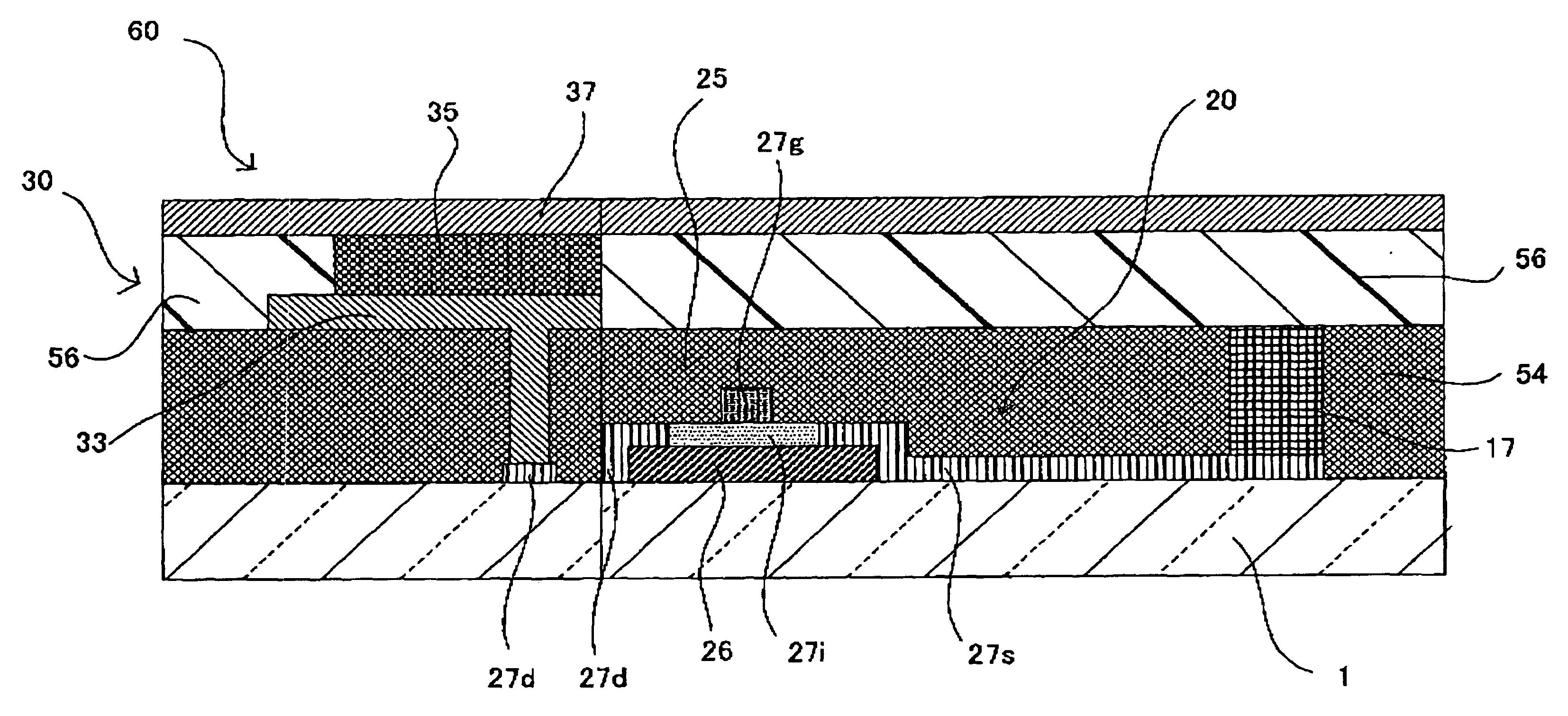
Figure 1 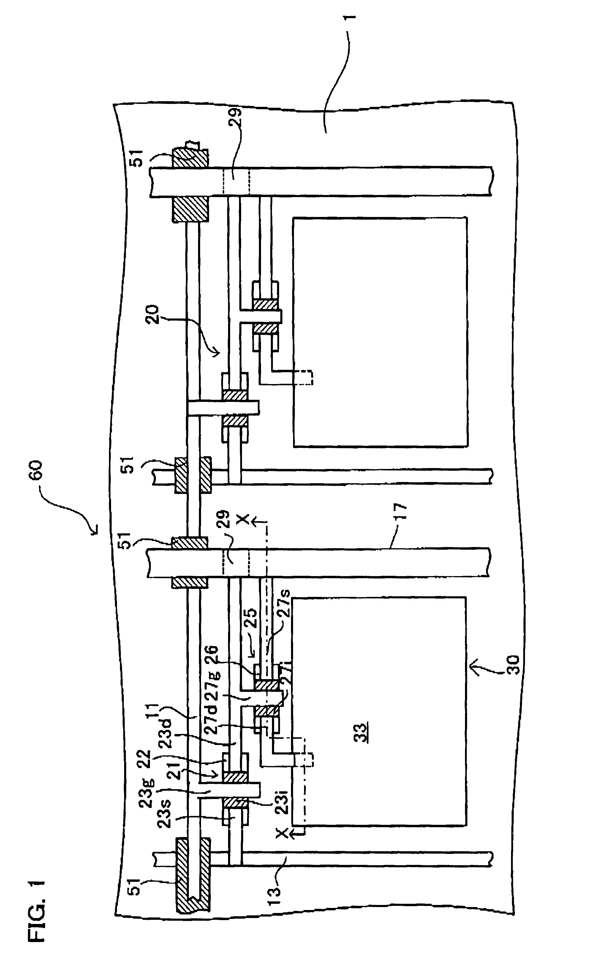
Figure 2 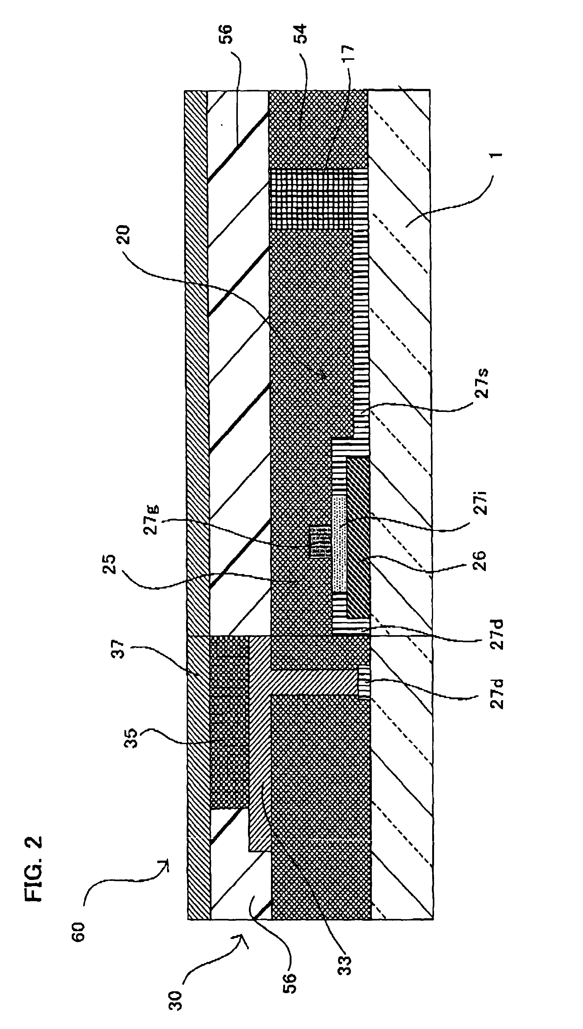
Figure 3
Abstract
Description
CROSS REFERENCE TO RELATED APPLICATIONThis application claims priority of Japanese Patent Application serial No. 2002-264555, filed Sep. 10, 2002.BACKGROUND OF THE INVENTION1. Field of the InventionThe present invention relates to a display using a current driven type light emitting element as a pixel, and to a method for manufacturing the same.2. Description of the Related ArtIn recent years, flat panel displays are used in many fields and in many places and, as computerization develops, the importance of them is increasingly enhanced.While, when we say a representative of the flat panel displays, it is a liquid crystal display (hereinafter referred to simply as “LCD”). As flat panel displays based on a displaying principle that is different from that of the LCD, development of organic electroluminescent (hereinafter the “electroluminescent” is abbreviated as “EL”) display, inorganic EL display, plasma display, light emitting diode display, fluorescent display tube, field emitting ...
Examples
example 1
As an example of the present invention, an active matrix organic EL display having a pixel circuit constitution illustrated in FIG. 8 was manufactured on a glass substrate by using a polysilicon film.
On a diagonal 17 inch substrate (size of 300 mm×370 mm), pixels were designed with a standard of XGA (768×1024).
First, pixel TFT, driver TFT circuit, and bus lines such as scanning lines and data signal lines were formed on the substrate. Then, a protective layer was formed with photo-sensitive acrylic resin, and through-holes which connects a source electrode and drain electrode of the driving TFT was formed. The film thickness of the protective layer was made 4 μm.
An ITO electrode was formed such that it may be connected to the drain via the through-hole on the drain side, and patterning was done to the pixel form. For forming the ITO electrode, a sputtering method was used.
Subsequently, a power source supply line was formed so as to be connected to the source via the through-hole on ...
example 2
As another Example of the present invention, except that the low molecular weight organic EL material that was used in Example 1 was replaced by a high molecular weight organic EL material, the same processes as those in Example 1 were performed. By this, the same effect as the Example 1 was obtained.
As the hole injection layer, PEDOT (polythiophen: Bayer CH8000) was coated to a thickness of 80 nm by spin coating and was baked at 160° C. to form the layer. A solution obtained by dissolving the following high molecular weight organic EL material into a solvent and liquefying was applied onto the PEDOT, using an ink jetting method, to make the three colors being juxtaposed, while CaAg was deposited as the cathode. A full color display was obtained.
(The Composition of the Organic EL Layer Forming Coating Solution)
Polyvinyl carbazole 70 weight partOxadiazole compound 30 weight partCoumarin 6 (fluorescent dye) 1 weight partMonochloro benzene (solvent)4900 weight part
In the case where th...