
Switching power supply circuit
a power supply circuit and switching converter technology, applied in the direction of electric variable regulation, process and machine control, instruments, etc., can solve the problems of high generation level of noise, damage to power factor indicative of power supply utilization efficiency, and inability to ignore the switching noise of the converter, so as to reduce the number of switching converter sections, reduce the number of parts, and reduce the effect of size and weigh
Patent Information
- Authority / Receiving Office
- US · United States
- Patent Type
- Patents(United States)
- Current Assignee / Owner
- Publication Date
- 2007-11-20
- Estimated Expiration
- Not applicable · inactive patent
Smart Images
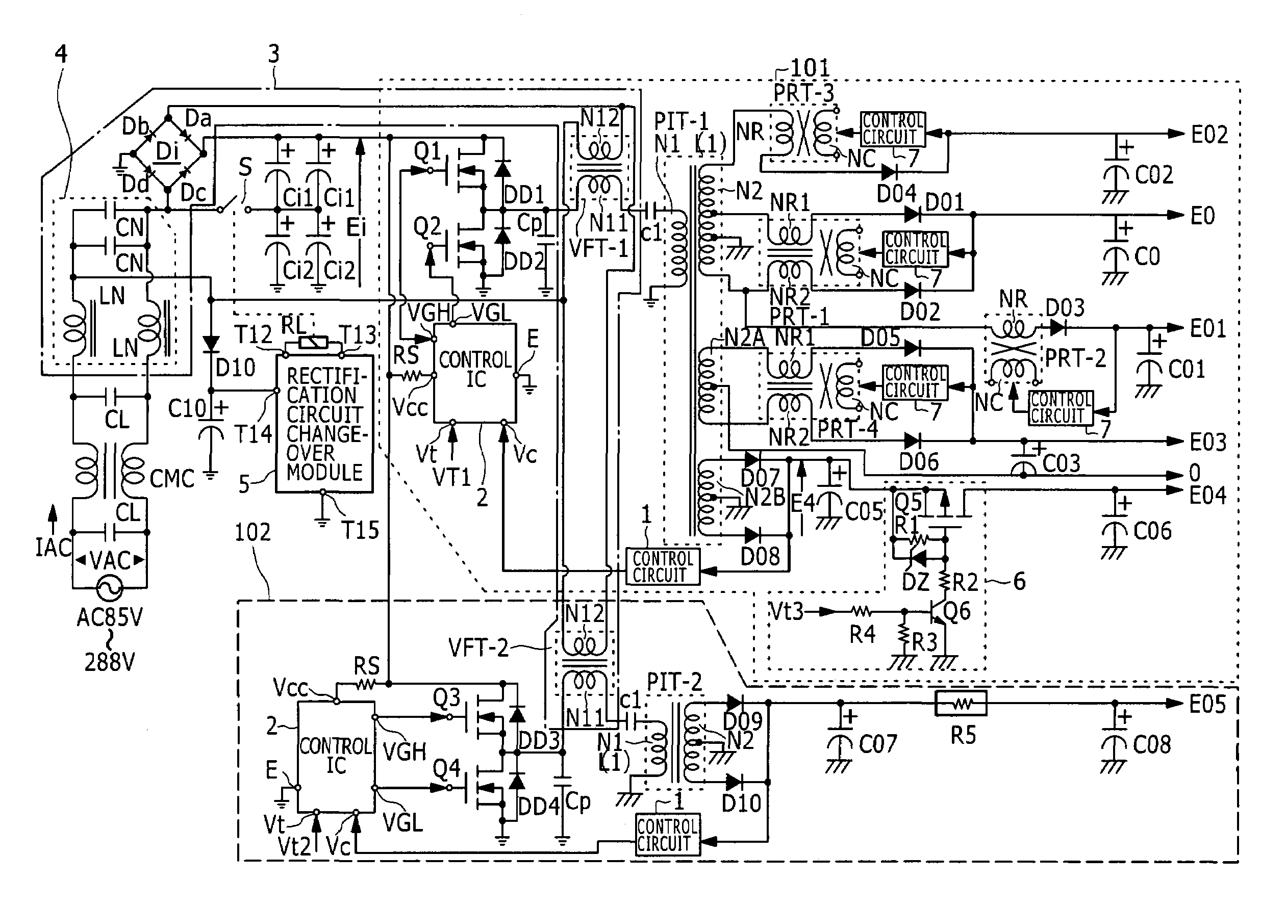
Figure 1 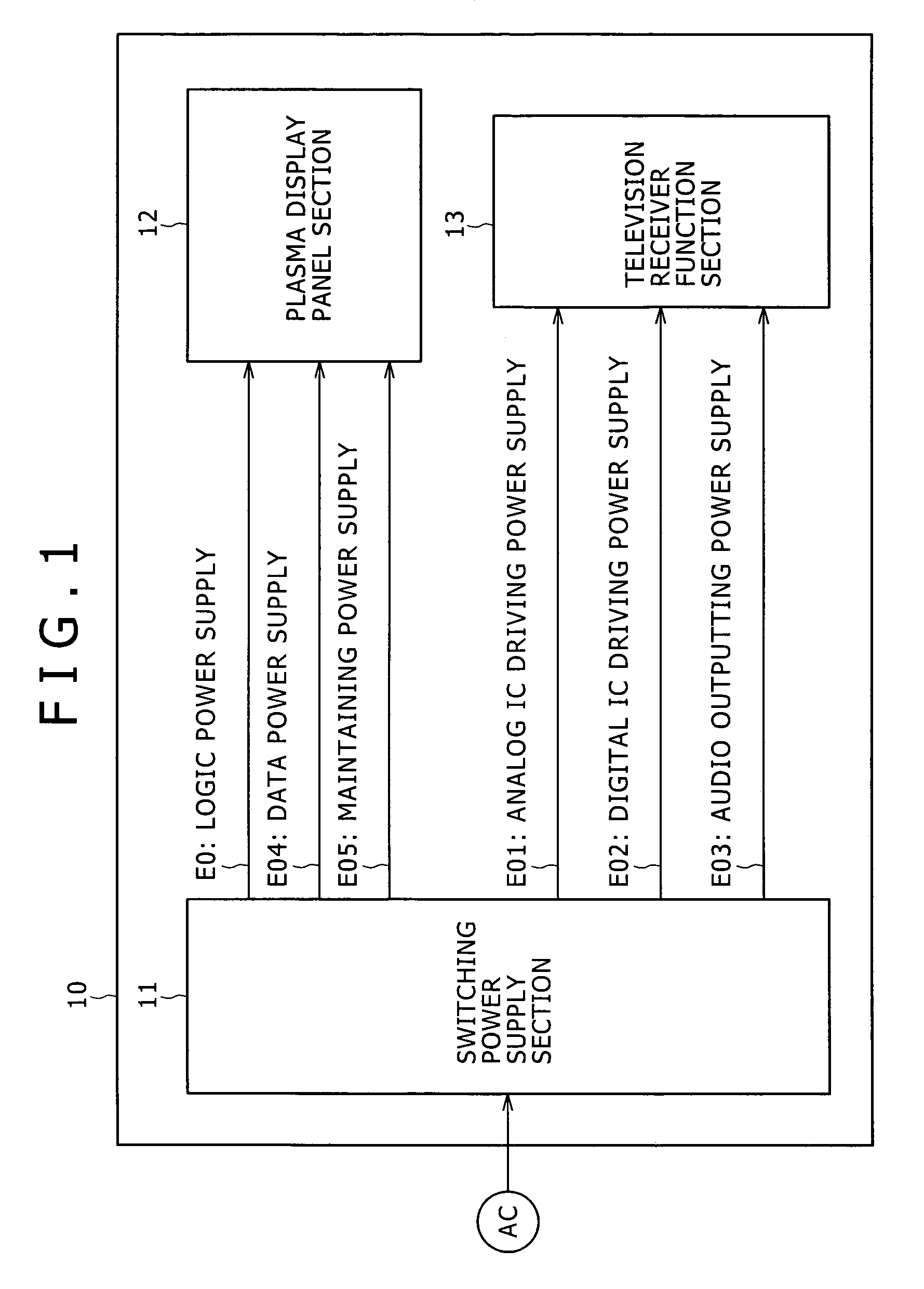
Figure 2 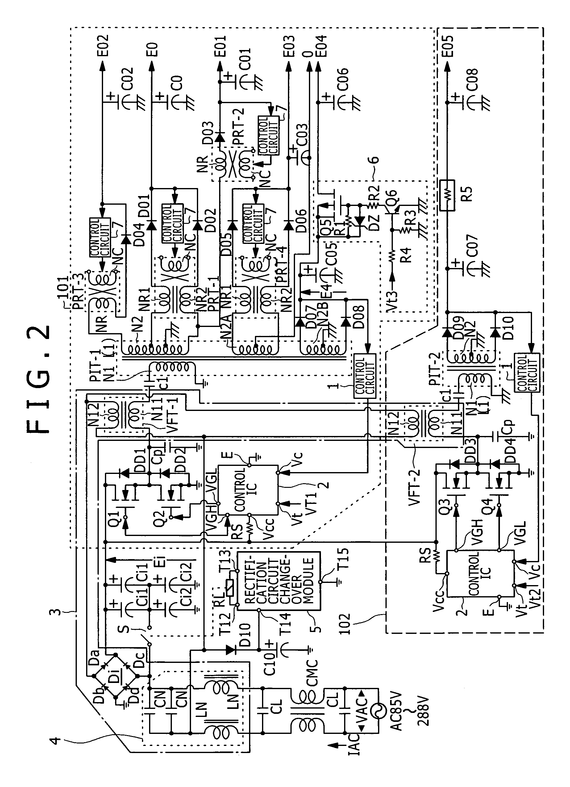
Figure 3
Abstract
Description
TECHNICAL FIELD
[0001] This invention relates to a switching power supply circuit including a circuit for the power factor improvement, and a plasma display apparatus which incorporates the switching power supply circuit.BACKGROUND ART
[0002] In recent years, since switching elements which can withstand comparatively high current and voltage of a high frequency have been developed, most of power supply circuits which rectify commercial power supply to obtain a desired DC voltage are formed as power supply circuits of the switching type.
[0003] A switching power supply circuit reduces the size of transformers and other devices by using a high switching frequency and is used as a high-power DC-DC converter and as a power supply for various kinds of electronic apparatus.
[0004] Incidentally, generally if commercial power supply is rectified, then since current flowing through a smoothing circuit is distorted in waveform, there is a problem that the power factor indicative of the utilization ef...
Examples
first embodiment
[0187]FIG. 2 shows an example of a configuration of a switching power supply circuit of the present invention as a switching power supply circuit which can be applied to the switching power supply circuit 11 shown in FIG. 1. The power supply circuit shown in FIG. 2 adopts a configuration which can be ready for the load power Po=600 W or more and operates with the AC 100 V system and the AC 200 V system of commercial AC power supply so that it is ready for a wide range.
[0188]In particular, the plasma display apparatus 10 as the present embodiment has so-called worldwide specifications such that it can operate in both of regions of the AC 100 V system of commercial power supply such as, for example, Japan and the United States and regions of the AC 200 V system such as Europe. Further, the power specification of the entire plasma display apparatus is generally 600 W or more.
[0189]In the power supply circuit shown in FIG. 2, a line filter formed from one common mode choke coil CMC and ...
second embodiment
[0340]FIG. 6 shows an example of a configuration of a switching power supply circuit as a It is to be noted that, in FIG. 6, like elements to those of FIG. 2 are denoted by like reference characters and description thereof is omitted herein.
[0341]In the power supply circuit shown in FIG. 6, firstly the internal configuration of the DC switch circuit (switch section) 6 provided on the first converter section 101 side is different from that in the case of FIG. 2. In particular, the DC switch circuit 6 includes a time constant capacitor C3. The power factor improving circuit 3 in this instance is formed from, for example, an electrolytic capacitor, and is connected at the positive terminal thereof to the base of the bipolar transistor Q6 and at the negative terminal thereof to the secondary side ground.
[0342]Further, in this instance, as an on / off control signal to be inputted to the DC switch circuit 6, the secondary side DC output voltage Eo5 of the second converter section 102 is i...