
In-plane switching mode liquid crystal display device having auxiliary pixel electrodes
a liquid crystal display and pixel electrode technology, applied in non-linear optics, instruments, optics, etc., can solve the problems of easy generation of signal interference, crosstalk and light leakage, and degrading the aperture ratio of the lcd, so as to prevent the generation of a disclination phenomenon in the pixel and the degradation of picture quality
Patent Information
- Authority / Receiving Office
- US · United States
- Patent Type
- Patents(United States)
- Current Assignee / Owner
- Publication Date
- 2012-04-17
Smart Images
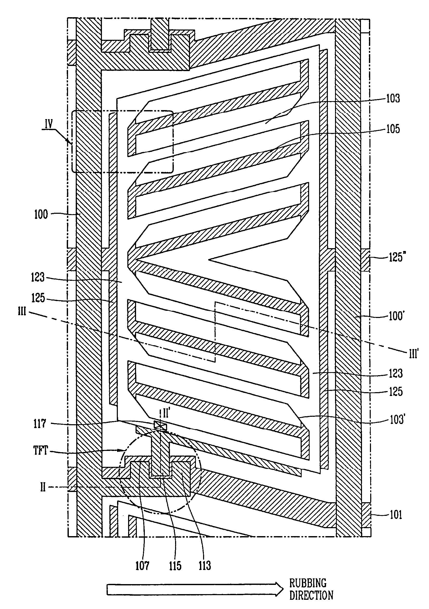
Figure 1 
Figure 2 
Figure 3
Abstract
Description
[0001] This application claims the benefit of Korean Patent Application No. 2004-117400, filed on Dec. 30, 2004, which is hereby incorporated by reference for all purposes as if fully set forth herein.BACKGROUND OF THE INVENTION
[0002] 1. Field of the Invention
[0003] The present invention relates to a liquid crystal display (LCD) device. More particularly, the present invention relates to an in-plane switching (IPS) mode LCD capable of preventing signal interference of a data line and reducing vertical line deficiency.
[0004] 2. Description of the Related Art
[0005] As various mobile electronic devices including a mobile phone, a PDA or a notebook computer are being developed, demands for light, thin, short and small flat panel display devices that can be applied to the mobile electronic devices are increasing. As a result, research for flat panel display devices such as an LCD (Liquid Crystal Display), PDP (Plasma Display Panel), an FED (Field Emission Display), a VFD (Vacuum Fluorescent D...
Examples
first embodiment
[0035]FIG. 3 shows a unit pixel of an LCD device in accordance with the present invention, and FIGS. 4A and 4B are sectional views taken along lines II-II′ and III-III′ of FIG. 3.
[0036]As illustrated, a liquid crystal panel includes a data line 100 and a gate line 101 arranged on a first substrate 110 and defining a unit pixel region, a switching device specifically, a TFT, disposed at a crossing of the gate line 101 and the data line 100, and at least one pixel electrode 103 and common electrode 105 alternately arranged in parallel in the pixel region and generating an in-plane field. Though not shown, an alignment film rubbed in a direction substantially perpendicular to the data line 200 is coated, and the pixel electrode 103 and the common electrode 105 are formed at a tilt angle of about 0°˜45° to the direction perpendicular to the data line 100.
[0037]The TFT includes a gate electrode 107 formed as a portion of the gate line 101 on the first substrate 110, a gate insulation fil...
third embodiment
[0057]FIG. 6 shows a unit pixel region of an LCD device in accordance with the present invention, in which both ends of a pixel electrode and a common electrode in a unit pixel region are bent.
[0058]The third embodiment of the present invention is similar to the first and second embodiment of the present invention. So only the differences will be described.
[0059]As illustrated in FIG. 6, a liquid crystal panel includes a data line 300 and a gate line 301 arranged on a first substrate and defining a unit pixel region, a TFT disposed at a crossing of the gate line 301 and the data line 300, and at least one pixel electrode 303 and common electrode 305 alternately arranged substantially parallel in the pixel region and generating an in-plane field of a first direction. The pixel electrode 303 and the common electrode 305 are formed at a tilt angle of about 0°˜45° in a direction substantially perpendicular to the data line 300. Both end regions (B) of the pixel electrode 303 and the com...