
Conductive pattern formation ink, conductive pattern and wiring substrate
a technology of conductive pattern and wiring substrate, which is applied in the direction of conductive layers on insulating supports, inks, printing, etc., can solve the problems of screen printing, miniaturization of wirings, and reduction of wiring pitch between wirings, so as to achieve high reliability
Patent Information
- Authority / Receiving Office
- US · United States
- Patent Type
- Patents(United States)
- Current Assignee / Owner
- Publication Date
- 2012-05-08
- Estimated Expiration
- Not applicable · inactive patent
Smart Images
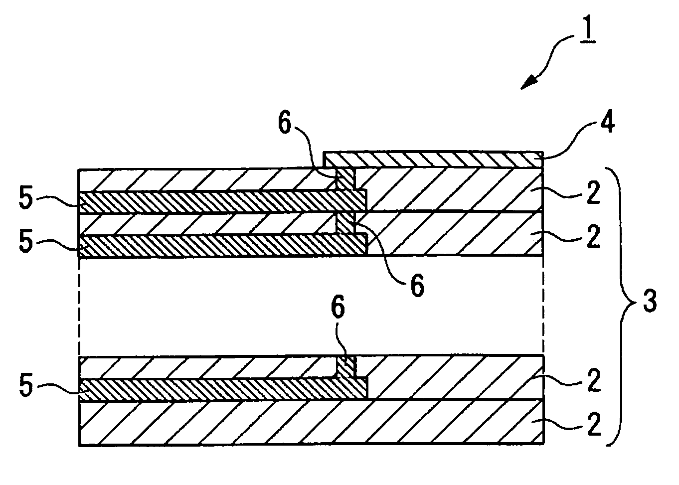
Figure 1 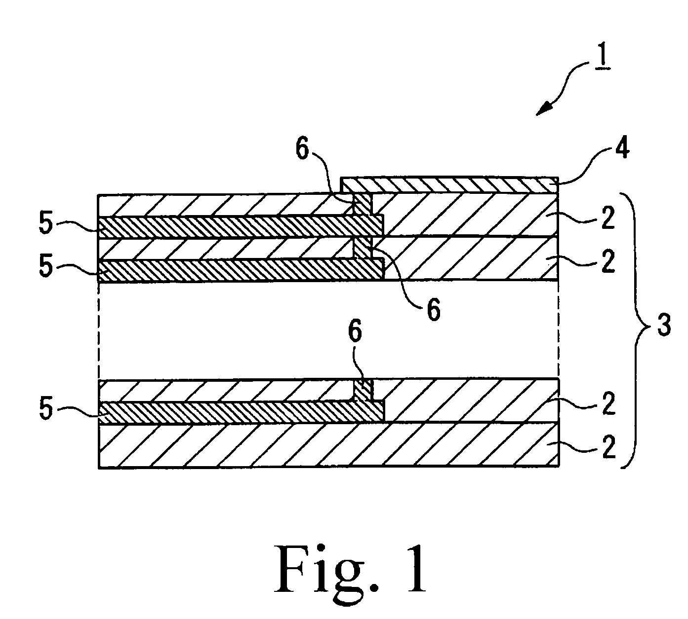
Figure 2 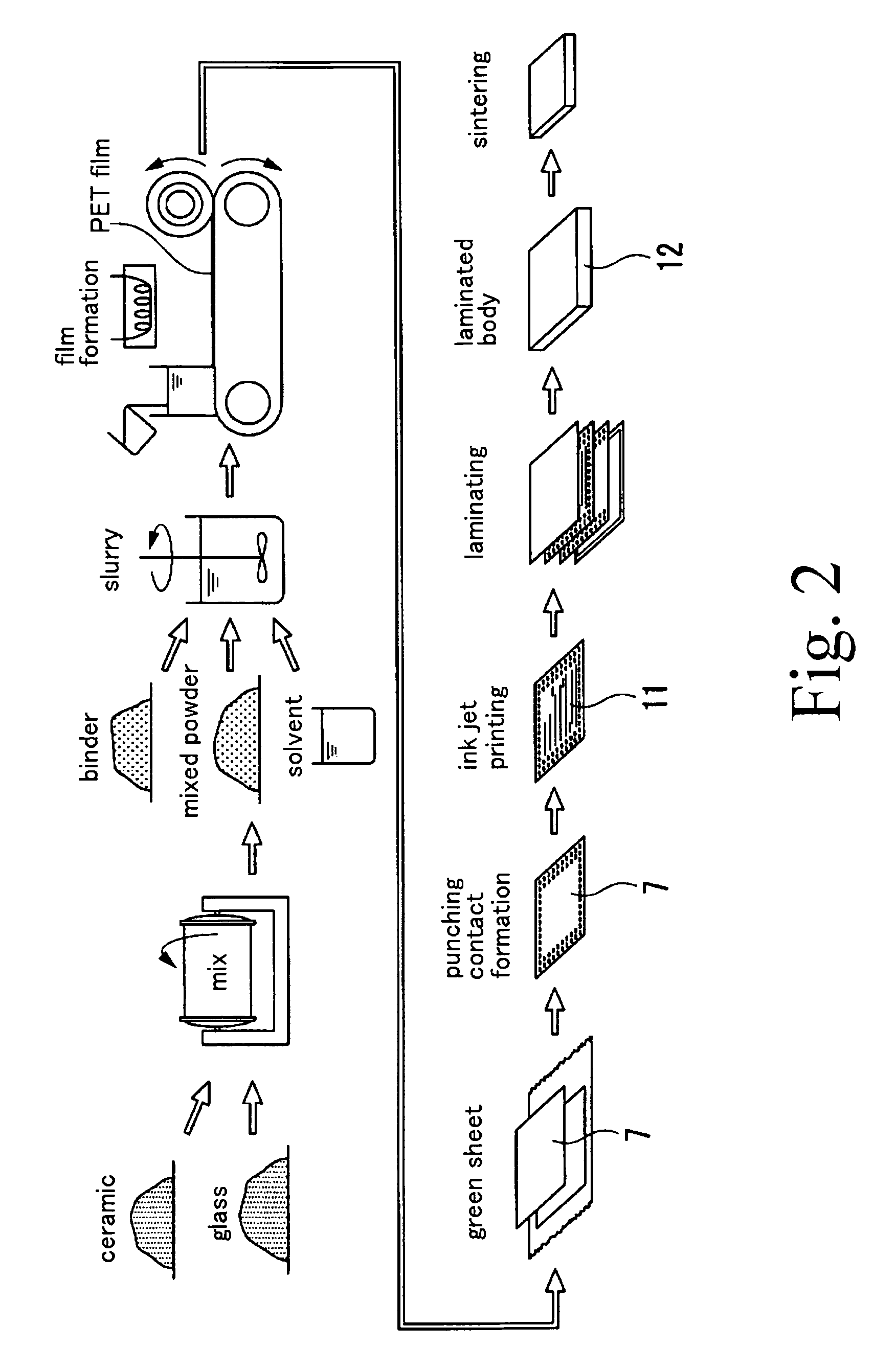
Figure 3
Abstract
Description
CROSS-REFERENCE TO RELATED APPLICATION
[0001] This application claims a priority to Japanese Patent Application No. 2007-320244 filed on Dec. 11, 2007 which is hereby expressly incorporated by reference herein in its entirety.BACKGROUND
[0002] 1. Technical Field
[0003] The present invention relates to a conductive pattern formation ink, a conductive pattern and a wiring substrate, and more specifically relates to a conductive pattern formation ink, a conductive pattern formed by the conductive pattern formation ink and a wiring substrate provided with the conductive pattern.
[0004] 2. Related Art
[0005] A ceramic circuit substrate including a substrate (a ceramic substrate) formed of a ceramic material and a wiring formed of a metal material and provided on the substrate has been widely used as a circuit substrate (a wiring substrate) on which electronic parts are to be mounted.
[0006] In such a ceramic circuit substrate, the substrate (the ceramic substrate) itself is formed of a multifunction...
Examples
example 1
[0347]17 g of trisodium citrate dihydrate and 0.36 g of tannic acid were dissolved in 50 mL of water alkalified by adding 3 mL of an aqueous 10N NaOH solution thereto, to obtain an aqueous solution. 3 mL of an aqueous 3.87 mol / L silver nitrate solution was added to the aqueous solution thus obtained drop by drop.
[0348]A silver colloid solution was obtained by stirring the above aqueous solution for two hours. The silver colloid solution thus obtained was dialyzed until conductivity thereof was decreased to 30 μS / cm or less, thereby desalting the silver colloid solution.
[0349]At the end of dialysis, coarse silver colloid particles were removed from the silver colloid solution by performing centrifugal separation at 3,000 rpm for 10 minutes.
[0350]Thereafter, a compound represented by the following formula (IV) as a surface tension adjuster, xylitol as a drying suppressant and a polyglycerin having a weight average molecular weight of 500 as a polyether compound were added to the silve...
examples 2 to 5
[0354]In each of Examples 2 to 5, a conductive pattern formation ink was prepared in the same manner as in the Example 1 except that the amount of the surface tension adjuster was changed as shown in Table 1.
example 6
[0355]A conductive pattern formation ink was prepared in the same manner as in the Example 1 except that the surface tension adjuster was changed from the compound represented by the above formula (IV) to a compound represented by the following formula (VI). In this regard, it is to be noted that a HLB value of the surface tension adjuster was 8.
[0356]
[0357]wherein m+n was 3.5