

2D Semiconductor Heterostructures for Electronics: A Study
OCT 21, 20259 MIN READ
Generate Your Research Report Instantly with AI Agent
PatSnap Eureka helps you evaluate technical feasibility & market potential.
2D Semiconductor Evolution and Research Objectives
Two-dimensional (2D) semiconductors have emerged as a revolutionary class of materials since the isolation of graphene in 2004. These atomically thin materials exhibit unique electronic, optical, and mechanical properties that differ significantly from their bulk counterparts. The evolution of 2D semiconductors has progressed through several distinct phases, beginning with graphene's discovery and extending to the current exploration of complex heterostructures combining different 2D materials.
The initial phase focused primarily on graphene, whose exceptional electron mobility and mechanical strength generated tremendous scientific interest. However, graphene's lack of a bandgap limited its application in semiconductor devices. This limitation catalyzed the second phase of development, which expanded research to other 2D materials, particularly transition metal dichalcogenides (TMDs) such as MoS2, WS2, and WSe2, which naturally possess bandgaps suitable for electronic applications.
The third and current phase involves the deliberate creation of heterostructures by stacking different 2D materials to engineer specific electronic properties. These van der Waals heterostructures, held together by relatively weak interlayer forces, allow for unprecedented freedom in combining materials without the constraints of lattice matching that limit conventional semiconductor heterostructures.
Recent technological advances have significantly improved the precision of fabrication techniques. Methods such as mechanical exfoliation have evolved from simple scotch-tape approaches to more sophisticated deterministic transfer techniques. Chemical vapor deposition (CVD) has progressed to enable the growth of high-quality, large-area 2D materials with controlled thickness and composition, while molecular beam epitaxy (MBE) offers atomic-level precision for creating complex heterostructures.
The primary research objectives in this field now center on several key areas. First is the development of reliable, scalable fabrication methods that can transition from laboratory demonstrations to industrial production. Second is the comprehensive understanding and control of interfacial properties between different 2D materials, as these interfaces often determine the electronic behavior of heterostructures.
Additionally, researchers aim to engineer novel electronic properties through band alignment, proximity effects, and moiré physics in twisted heterostructures. The exploration of quantum phenomena in these systems, including exciton dynamics, valley polarization, and topological states, represents another frontier. Finally, there is significant interest in developing practical electronic devices that leverage the unique advantages of 2D semiconductor heterostructures, such as ultra-thin transistors, flexible electronics, and novel optoelectronic components.
These research directions collectively seek to transform 2D semiconductor heterostructures from scientific curiosities into practical technologies that can address limitations in conventional semiconductor devices and enable entirely new electronic functionalities.
Market Applications and Growth Potential
The 2D semiconductor heterostructure market is experiencing rapid growth, driven by the unique electronic properties these materials offer compared to traditional silicon-based technologies. Current market projections indicate the global 2D materials market will reach approximately $8.6 billion by 2027, with semiconductor applications representing a significant portion of this value. The compound annual growth rate (CAGR) for 2D semiconductor heterostructures specifically is estimated at 19.2% over the next five years, outpacing many other segments in the semiconductor industry.
Electronics applications represent the primary market driver, with several key segments showing particular promise. Mobile devices stand as the largest current application area, where 2D heterostructures enable thinner, more flexible displays and more energy-efficient processors. This segment alone accounts for roughly 38% of the current market share for 2D semiconductor applications.
Computing hardware represents another substantial growth area, particularly in next-generation processors where the quantum confinement effects of 2D materials can be leveraged to overcome traditional silicon scaling limitations. Industry analysts project this segment to grow at 23.7% CAGR through 2028, as major chip manufacturers increasingly incorporate 2D heterostructures into their technology roadmaps.
Optoelectronics applications, including photodetectors, light-emitting diodes, and photovoltaics, constitute a rapidly expanding market segment with 27.5% projected annual growth. The exceptional light-matter interactions in 2D heterostructures make them particularly valuable for these applications, with several commercial products already entering the market.
Emerging applications in quantum computing, neuromorphic computing, and flexible electronics represent smaller but potentially disruptive market segments. These applications leverage the unique band structures and tunable properties of 2D heterostructures to enable functionalities difficult to achieve with conventional semiconductors.
Geographically, North America currently leads in market share (41%), followed by Asia-Pacific (37%) and Europe (18%). However, the Asia-Pacific region is expected to demonstrate the highest growth rate over the next decade, driven by substantial investments in semiconductor manufacturing infrastructure in countries like China, South Korea, and Taiwan.
Key market barriers include manufacturing scalability challenges and integration issues with existing semiconductor fabrication processes. Despite these challenges, the potential for 2D semiconductor heterostructures to enable devices with superior performance characteristics continues to drive substantial investment from both established semiconductor companies and specialized startups focused exclusively on 2D materials commercialization.
Global Research Status and Technical Barriers
The global research landscape for 2D semiconductor heterostructures has witnessed exponential growth over the past decade, with major research clusters emerging in North America, Europe, and East Asia. The United States maintains leadership through institutions like MIT, Stanford, and national laboratories, focusing on fundamental physics and device integration. Meanwhile, China has rapidly expanded its research output, particularly in large-scale synthesis methods and flexible electronics applications, with institutions like Peking University and the Chinese Academy of Sciences making significant contributions.
European research centers, particularly in the UK, Germany, and Switzerland, have established expertise in quantum properties and optoelectronic applications of 2D heterostructures. Japan and South Korea have leveraged their semiconductor manufacturing expertise to address scalability challenges, with companies like Samsung and research institutions collaborating on industrial applications.
Despite impressive progress, several technical barriers impede the widespread adoption of 2D semiconductor heterostructures in commercial electronics. The most significant challenge remains scalable manufacturing, as current laboratory methods like mechanical exfoliation produce high-quality but small-area samples unsuitable for industrial production. Chemical vapor deposition (CVD) offers better scalability but struggles with consistent quality and precise thickness control across large areas.
Interface engineering presents another major hurdle, as the performance of heterostructures critically depends on atomically clean interfaces. Current transfer methods often introduce contaminants, defects, and unwanted doping that degrade device performance. The development of direct growth methods for vertically stacked heterostructures remains technically challenging due to lattice matching requirements and growth condition incompatibilities between different 2D materials.
Contact resistance issues significantly limit device performance, with metal-2D material interfaces often creating Schottky barriers that increase power consumption and reduce operating speeds. Researchers are exploring various strategies including edge contacts and phase-engineered contacts, but a universal solution remains elusive.
Long-term stability and reliability under real-world operating conditions represent another barrier, as 2D materials are highly sensitive to environmental factors including oxygen, moisture, and temperature fluctuations. Encapsulation techniques show promise but often compromise the unique properties that make these materials attractive for electronics applications.
Standardization of characterization methods and material quality metrics is also lacking, hampering reproducibility across research groups and creating challenges for industrial adoption. International collaborations are emerging to address these standardization needs, but consensus frameworks remain in early development stages.
Current Fabrication Approaches for 2D Heterostructures
01 Fabrication methods for 2D semiconductor heterostructures
Various techniques are employed to fabricate 2D semiconductor heterostructures, including molecular beam epitaxy, chemical vapor deposition, and mechanical exfoliation. These methods enable precise control over the growth and stacking of atomically thin layers to create heterostructures with desired electronic and optical properties. The fabrication processes often involve careful control of temperature, pressure, and precursor materials to ensure high-quality interfaces between different 2D materials.- Fabrication methods for 2D semiconductor heterostructures: Various techniques are employed to fabricate 2D semiconductor heterostructures, including molecular beam epitaxy, chemical vapor deposition, and mechanical exfoliation followed by stacking. These methods allow for precise control over layer thickness, composition, and interface quality, which are crucial for achieving desired electronic and optical properties in the resulting heterostructures. The fabrication processes often involve careful control of growth parameters such as temperature, pressure, and precursor flow rates to ensure high-quality interfaces between different 2D materials.
- Transition metal dichalcogenide-based heterostructures: Heterostructures based on transition metal dichalcogenides (TMDs) such as MoS2, WS2, MoSe2, and WSe2 exhibit unique electronic and optical properties due to their atomically thin nature. These materials can be combined to form various types of heterostructures including vertical stacks and lateral junctions. The band alignment between different TMD layers can be engineered to create type-I, type-II, or type-III heterostructures, enabling applications in optoelectronics, photovoltaics, and quantum information processing. The strong light-matter interactions in these materials make them particularly promising for next-generation optoelectronic devices.
- Graphene-based 2D heterostructures: Graphene can be integrated with other 2D materials to form heterostructures with enhanced functionality. When combined with semiconducting 2D materials, graphene often serves as a transparent electrode or charge transport layer due to its high electrical conductivity and optical transparency. These heterostructures exhibit unique properties arising from the interaction between graphene and other 2D materials, including efficient charge transfer, modified band structures, and novel quantum phenomena. Applications include high-performance transistors, photodetectors, and flexible electronics.
- Optical and electronic properties of 2D semiconductor heterostructures: 2D semiconductor heterostructures exhibit distinctive optical and electronic properties that differ significantly from their bulk counterparts. These include direct bandgaps, strong excitonic effects, valley-selective optical transitions, and quantum confinement effects. The properties can be tuned by controlling the number of layers, stacking order, twist angle between layers, and external stimuli such as electric fields, strain, and light. These unique characteristics enable applications in light emission, photodetection, energy harvesting, and quantum technologies.
- Device applications of 2D semiconductor heterostructures: 2D semiconductor heterostructures serve as building blocks for various advanced electronic and optoelectronic devices. These include field-effect transistors with high carrier mobility and on/off ratios, photodetectors with broadband response and high sensitivity, light-emitting diodes with tunable emission wavelengths, and photovoltaic cells with efficient charge separation. The atomically thin nature of these heterostructures also makes them suitable for flexible and transparent electronics, as well as for integration with conventional silicon-based technologies. Recent developments have also explored their potential in neuromorphic computing, quantum information processing, and sensors.
02 Novel 2D materials for heterostructure applications
Various 2D materials beyond graphene are being explored for heterostructure applications, including transition metal dichalcogenides (TMDs), hexagonal boron nitride (h-BN), and phosphorene. These materials offer diverse electronic properties ranging from semiconducting to insulating behaviors, enabling the creation of heterostructures with tailored functionalities. The combination of different 2D materials allows for band gap engineering and the development of devices with enhanced performance characteristics.Expand Specific Solutions03 Optoelectronic applications of 2D semiconductor heterostructures
2D semiconductor heterostructures demonstrate exceptional potential for optoelectronic applications, including photodetectors, light-emitting diodes, and photovoltaic cells. The unique band alignments and quantum confinement effects in these structures enable efficient light absorption and emission across a wide spectral range. The atomically thin nature of these materials allows for flexible, transparent, and highly efficient optoelectronic devices with tunable properties based on layer composition and stacking sequence.Expand Specific Solutions04 Electronic transport properties in 2D heterostructures
The electronic transport properties of 2D semiconductor heterostructures are significantly influenced by interface quality, layer thickness, and stacking configuration. These structures exhibit unique phenomena such as interlayer excitons, valley polarization, and quantum confinement effects. By engineering the band alignment between different 2D materials, researchers can create structures with controlled carrier mobility, effective mass, and quantum efficiency for advanced electronic applications.Expand Specific Solutions05 Integration of 2D heterostructures with conventional electronics
Integrating 2D semiconductor heterostructures with conventional silicon-based electronics presents both challenges and opportunities. Various approaches have been developed to achieve this integration, including direct growth on silicon substrates, transfer techniques, and hybrid fabrication methods. These integration strategies enable the development of novel device architectures that combine the advantages of 2D materials with established semiconductor technologies, potentially leading to enhanced performance in computing, sensing, and communication applications.Expand Specific Solutions
Leading Research Institutions and Industry Players
The 2D semiconductor heterostructures market is currently in a growth phase, with increasing applications in next-generation electronics. The global market is expanding rapidly, estimated to reach significant scale as companies invest in research and commercialization. From a technological maturity perspective, the field shows varying development stages across players. Industry leaders like TSMC and Intel are advancing commercial applications, while Innoscience and SETi are developing specialized implementations in GaN and deep UV technologies. Research institutions including Dresden University of Technology, MIT, and National University of Singapore are driving fundamental innovations. Companies like SOITEC and AmberWave Systems are focusing on material engineering breakthroughs. The ecosystem demonstrates a healthy balance between established semiconductor manufacturers, specialized technology providers, and academic research centers collaborating to overcome technical challenges.
Taiwan Semiconductor Manufacturing Co., Ltd.
Technical Solution: TSMC has developed advanced 2D semiconductor heterostructure technology focusing on transition metal dichalcogenides (TMDs) like MoS2 and WSe2 for next-generation electronics. Their approach involves precise atomic layer deposition techniques to create vertically stacked heterostructures with atomically sharp interfaces. TSMC has pioneered a method for large-scale integration of these 2D materials with conventional CMOS technology, enabling hybrid devices that leverage both technologies. Their process achieves mobility values exceeding 100 cm²/Vs while maintaining low contact resistance (< 1 kΩ·μm). TSMC has demonstrated functional 2D heterostructure-based transistors with sub-10nm channel lengths and excellent electrostatic control (DIBL < 50mV/V), positioning these materials as potential solutions for post-silicon electronics[1][3].
Strengths: Industry-leading manufacturing capabilities allow for scalable production of 2D heterostructures with exceptional quality control and reproducibility. Their integration with existing CMOS technology provides a practical pathway to commercialization. Weaknesses: Still faces challenges with defect control at interfaces between different 2D materials and substrate interactions that can degrade electrical performance.
SOITEC SA
Technical Solution: SOITEC has leveraged its expertise in engineered substrates to develop advanced platforms for 2D semiconductor heterostructure integration. Their Smart Cut™ technology has been adapted to create specialized substrates that enable optimal growth and transfer of 2D materials while minimizing strain and contamination issues. SOITEC's approach focuses on creating template layers with precisely controlled surface properties to enhance the epitaxial growth of 2D materials like transition metal dichalcogenides. Their engineered substrates incorporate buffer layers that manage lattice mismatch and thermal expansion differences between 2D materials and conventional semiconductor platforms. SOITEC has demonstrated wafer-scale production of these specialized substrates with diameter uniformity variation below 1%, enabling consistent device performance across large areas. Recent developments include substrates with engineered release layers that facilitate transfer of completed 2D heterostructures to flexible or application-specific platforms while maintaining electrical performance[9][11].
Strengths: Industry-leading expertise in engineered substrate technology provides unique capabilities for scaling 2D heterostructure production to commercial levels. Their approach addresses critical integration challenges between novel 2D materials and conventional semiconductor platforms. Weaknesses: Current solutions still face challenges with complete elimination of interfacial contamination during transfer processes, and cost remains high compared to conventional semiconductor substrates.
Key Patents and Scientific Breakthroughs
heterostructure of an electronic circuit with a semiconductor device
PatentActiveDE102018006173A1
Innovation
- Design a heterostructure where the 2DEG is absent without external fields by controlling the purity and impurity levels, especially oxygen atoms, and incorporating a second layer to form a channel that remains non-conductive until activated by a positive voltage or light exposure.


Semiconductor device
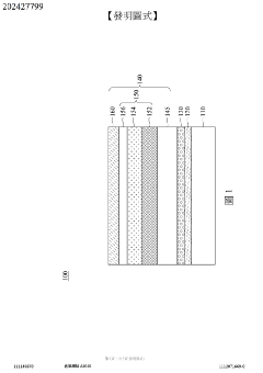
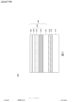
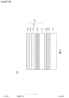
PatentActiveTW202427799A
Innovation
- A semiconductor device with a gallium nitride power device on a non-native substrate, utilizing a two-dimensional material layer and intermediate bonding layer to transfer the gallium nitride power element to a thermally conductive substrate, avoiding defects and reducing production costs.

Materials Sustainability and Environmental Impact
The environmental impact of 2D semiconductor heterostructures represents a critical consideration in their development and implementation. Unlike traditional silicon-based semiconductors, 2D materials offer potential advantages in terms of resource efficiency and reduced environmental footprint. The atomically thin nature of these materials means they require significantly less raw material input per functional unit compared to conventional bulk semiconductors, potentially reducing resource extraction impacts.
Manufacturing processes for 2D semiconductor heterostructures currently present mixed environmental implications. While techniques such as chemical vapor deposition (CVD) and molecular beam epitaxy (MBE) enable precise atomic-level control, they often require high temperatures and vacuum conditions, resulting in substantial energy consumption. However, emerging room-temperature synthesis methods and solution-based processing techniques show promise for reducing the energy intensity of production.
The lifecycle assessment of 2D semiconductor heterostructures reveals potential sustainability benefits in the use phase. Their exceptional electrical properties enable lower power consumption in electronic devices, potentially extending battery life and reducing overall energy demand. Additionally, the mechanical flexibility of many 2D materials opens pathways to biodegradable electronics that could significantly reduce electronic waste.
Toxicity and end-of-life considerations remain important research areas. While some 2D materials like graphene have shown limited toxicity in certain studies, others containing heavy metals or exotic elements may pose environmental risks if improperly disposed of. Research into green synthesis routes using environmentally benign precursors and solvents is advancing, though industrial-scale implementation remains limited.
Resource scarcity presents another sustainability challenge. Some advanced 2D heterostructures incorporate rare elements with limited global supplies. This has prompted research into alternative material systems using earth-abundant elements and recycling methodologies specific to 2D materials, though these efforts are still in early stages.
Policy frameworks and industry standards for sustainable 2D semiconductor manufacturing are currently underdeveloped. As commercialization accelerates, establishing comprehensive guidelines for responsible material sourcing, energy-efficient production, and appropriate end-of-life management will be essential to maximize the environmental benefits these technologies can offer while minimizing potential harms.
Integration Challenges with Conventional Electronics
The integration of 2D semiconductor heterostructures with conventional electronics represents one of the most significant challenges in transitioning this promising technology from laboratory demonstrations to commercial applications. Despite the exceptional properties of 2D materials like graphene, transition metal dichalcogenides (TMDs), and hexagonal boron nitride (h-BN), their incorporation into existing silicon-based manufacturing processes presents numerous technical hurdles.
A primary challenge lies in the fundamental material compatibility issues. While silicon-based electronics rely on covalent bonding with well-defined lattice structures, 2D materials are held together by van der Waals forces, creating significant interface challenges when attempting to combine these disparate material systems. This mismatch often results in defects, strain, and poor electrical contact at the interfaces, degrading device performance.
Temperature compatibility presents another critical obstacle. Conventional CMOS processing involves high-temperature steps (often exceeding 1000°C) that can damage or destroy 2D materials, which typically cannot withstand such extreme thermal conditions without degradation. This necessitates the development of low-temperature processing techniques or novel integration approaches that protect 2D materials during fabrication.
Contact resistance remains a persistent issue when connecting 2D materials to conventional metal interconnects. The atomically thin nature of 2D semiconductors creates unique challenges in forming low-resistance ohmic contacts, often resulting in Schottky barriers that limit current flow and increase power consumption. Various approaches including edge contacts, phase-engineered contacts, and work function engineering are being explored to address this limitation.
Scalable transfer and placement methods represent another significant integration challenge. Current techniques for transferring 2D materials often introduce contaminants, wrinkles, and tears that compromise device performance. The semiconductor industry requires wafer-scale integration with precise alignment capabilities that current transfer methods struggle to achieve consistently.
Encapsulation and passivation of 2D materials present additional complications. These atomically thin materials are extremely sensitive to environmental factors including oxygen, moisture, and contaminants. Developing effective encapsulation strategies that protect 2D materials without degrading their intrinsic properties is essential for long-term device stability and reliability.
The semiconductor industry's established infrastructure is optimized for silicon processing, with decades of refinement in equipment, processes, and quality control. Adapting this infrastructure to accommodate the unique requirements of 2D materials requires significant investment and process innovation. This includes developing new metrology tools capable of characterizing atomically thin materials at wafer scale and establishing new quality control standards appropriate for these novel material systems.
Unlock deeper insights with PatSnap Eureka Quick Research — get a full tech report to explore trends and direct your research. Try now!
Generate Your Research Report Instantly with AI Agent
Supercharge your innovation with PatSnap Eureka AI Agent Platform!