3D Stacking of Memory and Logic using GAA for Neuromorphic SoCs.
SEP 8, 20259 MIN READ
Generate Your Research Report Instantly with AI Agent
Patsnap Eureka helps you evaluate technical feasibility & market potential.
3D Stacking Evolution and Objectives
The evolution of 3D stacking technology represents a significant paradigm shift in semiconductor integration, moving from traditional 2D planar architectures to vertically stacked structures. This transition began in the early 2000s with the introduction of basic package-on-package (PoP) solutions, followed by through-silicon via (TSV) technology which enabled more direct vertical interconnections between stacked dies. The subsequent development of interposer-based 2.5D integration served as an intermediate step, allowing heterogeneous integration of multiple chips on a silicon substrate.
Recent advancements have led to true 3D integration with die-to-die and wafer-to-wafer bonding techniques, significantly reducing interconnect lengths and improving overall system performance. The integration of memory and logic in 3D stacks has been particularly transformative, addressing the memory wall challenge by bringing memory closer to processing elements, thereby reducing latency and power consumption associated with data movement.
The emergence of Gate-All-Around (GAA) transistor technology represents the next evolution in semiconductor device architecture, offering superior electrostatic control compared to FinFET technology. GAA's cylindrical channel design enables continued scaling beyond 5nm nodes while maintaining performance improvements and power efficiency. This technology is particularly valuable for neuromorphic computing applications, which demand high computational density and energy efficiency.
The primary objectives of 3D stacking of memory and logic using GAA for Neuromorphic SoCs are multifaceted. First, to achieve unprecedented levels of integration density, enabling more complex neuromorphic architectures that better mimic biological neural networks. Second, to dramatically reduce power consumption by minimizing data movement between memory and processing elements, a critical requirement for edge AI applications where power constraints are significant.
Third, to enhance system performance through reduced interconnect delays and increased bandwidth between memory and logic components. Fourth, to enable heterogeneous integration of different technologies optimized for specific functions, such as non-volatile memory arrays for synaptic weight storage alongside high-performance logic for neural processing. Fifth, to improve thermal management through advanced cooling solutions and optimized heat dissipation pathways in 3D structures.
The ultimate goal is to create neuromorphic systems-on-chip that can approach the energy efficiency and computational capabilities of biological brains, potentially enabling a new generation of AI applications that can operate effectively under strict power and form factor constraints. This convergence of 3D stacking and GAA technology represents a promising pathway toward realizing the full potential of neuromorphic computing.
Market Analysis for Neuromorphic Computing
The neuromorphic computing market is experiencing significant growth, driven by the increasing demand for AI applications that require efficient processing of complex neural networks. Current market valuations place the global neuromorphic computing sector at approximately 3.2 billion USD in 2023, with projections indicating a compound annual growth rate (CAGR) of 24.7% through 2030. This remarkable growth trajectory is fueled by advancements in hardware architectures like 3D stacking of memory and logic using Gate-All-Around (GAA) technology for neuromorphic System-on-Chips (SoCs).
Key market segments demonstrating strong demand include autonomous vehicles, robotics, healthcare diagnostics, and edge computing applications. The automotive sector alone is expected to contribute over 1.5 billion USD to the neuromorphic computing market by 2027, as manufacturers increasingly integrate advanced driver assistance systems and autonomous driving capabilities that benefit from brain-inspired computing architectures.
Healthcare applications represent another substantial growth area, with neuromorphic solutions enabling more efficient processing of medical imaging data and real-time patient monitoring. Market research indicates this segment is growing at 29.3% annually, outpacing the overall market average.
From a geographical perspective, North America currently dominates the neuromorphic computing market with approximately 42% market share, followed by Europe (27%) and Asia-Pacific (23%). However, the Asia-Pacific region is demonstrating the fastest growth rate at 28.1% annually, driven by substantial investments in AI infrastructure in China, Japan, and South Korea.
The enterprise adoption curve shows neuromorphic computing is transitioning from early adopter phase to early majority, with 18% of Fortune 500 companies actively exploring or implementing neuromorphic solutions in their technology roadmaps. This represents a 7% increase from 2021, indicating accelerating commercial interest.
Market challenges include high initial implementation costs, with average neuromorphic hardware solutions priced 3-5 times higher than traditional computing architectures. Additionally, the ecosystem remains fragmented, with limited standardization across hardware platforms and programming frameworks.
Demand forecasts suggest the market for specialized neuromorphic SoCs utilizing 3D stacking and GAA technology will grow at 31.2% annually through 2028, outpacing the broader neuromorphic segment. This accelerated growth is attributed to the superior power efficiency and performance density these architectures offer for edge AI applications, where power constraints are particularly stringent.
GAA Technology Status and Barriers
Gate-All-Around (GAA) transistor technology represents a significant evolution beyond FinFET architecture, offering enhanced electrostatic control and scalability for advanced semiconductor nodes. Currently, GAA technology has progressed from research laboratories to early production stages, with major semiconductor manufacturers including Samsung, TSMC, and Intel incorporating GAA transistors in their roadmaps for 3nm nodes and beyond. Samsung's 3nm process utilizing Multi-Bridge-Channel FET (MBCFET), a variant of GAA, demonstrates the commercial viability of this technology.
Despite this progress, GAA technology faces substantial barriers when applied to 3D stacking for neuromorphic SoCs. The primary challenge lies in thermal management, as the vertical integration of memory and logic layers creates significant heat dissipation issues. The increased transistor density in GAA architectures exacerbates this problem, potentially leading to performance degradation and reliability concerns in neuromorphic applications that require consistent computational capabilities.
Manufacturing complexity presents another major barrier. The fabrication of GAA transistors requires precise control of nanowire or nanosheet formation, with channel dimensions approaching sub-5nm. When integrated into 3D stacked architectures, the complexity multiplies due to the need for ultra-precise alignment between layers and the formation of high-aspect-ratio through-silicon vias (TSVs) that maintain signal integrity across the stack.
Power delivery networks face unique challenges in GAA-based 3D stacked neuromorphic SoCs. The increased resistance in nanowire/nanosheet structures combined with the complex power distribution requirements across multiple stacked layers creates voltage drop issues that can affect the timing and functionality of neuromorphic circuits, which are particularly sensitive to signal timing variations.
Yield management represents a critical barrier, as defect densities in GAA processes remain higher than mature FinFET technologies. When combined with 3D stacking, the compound yield impact becomes a significant economic concern, potentially limiting mass production viability for neuromorphic applications.
From a design perspective, electronic design automation (EDA) tools are still evolving to fully support GAA-based 3D architectures. Current tools lack comprehensive capabilities for thermal-aware placement and routing across multiple stacked layers with GAA transistors, creating bottlenecks in the development pipeline for neuromorphic SoCs.
Material innovation challenges also persist, particularly regarding the interface materials between stacked layers and the channel materials for GAA transistors that can maintain performance while operating within the thermal constraints of 3D stacked environments. Silicon-germanium and pure germanium channels show promise but introduce additional process complexity.
Current 3D Stacking Architectures
01 3D Integration of GAA Transistors with Memory
This approach involves the vertical stacking of gate-all-around (GAA) transistors with memory components to create high-density 3D integrated circuits. The GAA structure provides better electrostatic control and reduced short-channel effects compared to traditional transistor designs. By integrating memory directly with logic using GAA technology, these architectures achieve improved performance, reduced interconnect delays, and better power efficiency in a compact form factor.- 3D integration of GAA transistors with memory: This approach involves the vertical stacking of gate-all-around (GAA) transistors with memory components to create 3D integrated circuits. The GAA structure provides better electrostatic control and reduced short-channel effects compared to traditional transistor designs. By stacking memory layers on top of logic layers containing GAA transistors, manufacturers can achieve higher density, improved performance, and reduced power consumption in semiconductor devices.
- Monolithic 3D integration techniques for memory and logic: Monolithic 3D integration enables the fabrication of multiple active layers on a single chip, allowing for the vertical stacking of memory and logic components. This technique involves sequential processing of device layers rather than bonding separate wafers. For GAA devices, specialized fabrication processes ensure proper alignment and interconnection between the memory and logic layers. This approach reduces interconnect length, improves performance, and enables higher integration density compared to traditional 2D integration.
- Thermal management in 3D stacked GAA memory-logic systems: Thermal management is critical in 3D stacked structures due to the increased power density and heat generation. Various techniques are employed to address thermal challenges in GAA-based 3D memory-logic integration, including the use of thermal vias, heat spreaders, and optimized floorplanning. Advanced cooling solutions and thermally-aware design methodologies help maintain device reliability and performance by preventing excessive temperature rise in the stacked structure.
- Interconnect architecture for 3D GAA memory-logic integration: Specialized interconnect architectures are essential for effective communication between stacked memory and logic layers in 3D GAA systems. These architectures include through-silicon vias (TSVs), monolithic inter-tier vias, and advanced routing schemes that minimize signal delay and power consumption. The interconnect design must address challenges related to alignment, density, and electrical performance while enabling high-bandwidth communication between the memory and logic components.
- Design optimization and manufacturing techniques for 3D GAA integration: Design optimization and specialized manufacturing techniques are crucial for successful implementation of 3D stacked GAA memory-logic systems. This includes process integration strategies, design-for-manufacturing considerations, and yield enhancement techniques. Advanced lithography, etching, and deposition methods are employed to fabricate the complex GAA structures in a 3D configuration. Design tools and methodologies specifically tailored for 3D integration help optimize performance, power, and area while addressing manufacturing challenges.
02 Monolithic 3D Integration Techniques
Monolithic 3D integration enables the fabrication of memory and logic components in multiple layers on a single chip. This technique involves sequential processing of device layers rather than bonding separate wafers. The approach allows for high-density vertical interconnects between memory and logic layers, significantly reducing wire length and improving performance. Advanced processes include layer transfer techniques, sequential fabrication, and specialized thermal management to handle the integration challenges.Expand Specific Solutions03 Thermal Management and Process Integration
Effective thermal management is critical in 3D stacked memory-logic structures using GAA technology. The integration process must address thermal challenges arising from stacking multiple active layers. Solutions include the incorporation of thermal vias, heat-dissipating materials, and optimized layout designs. Process integration techniques focus on maintaining low thermal budgets for upper layers to prevent degradation of previously fabricated devices while ensuring proper electrical connections between memory and logic components.Expand Specific Solutions04 Interconnect Architecture for 3D Memory-Logic Integration
Specialized interconnect architectures are developed to optimize the communication between stacked memory and logic layers using GAA technology. These architectures include high-density through-silicon vias (TSVs), monolithic inter-tier vias, and advanced routing schemes. The interconnect design focuses on minimizing latency, reducing power consumption, and maximizing bandwidth between memory and logic components while maintaining signal integrity across the 3D structure.Expand Specific Solutions05 Design Optimization and Performance Enhancement
Design optimization techniques for 3D stacked memory-logic systems with GAA technology focus on maximizing performance while addressing physical constraints. These include circuit partitioning strategies, memory-logic co-design methodologies, and system-level optimization. Performance enhancements are achieved through reduced wire lengths, optimized placement of critical components, and specialized circuit designs that leverage the unique capabilities of GAA transistors in a 3D integrated environment.Expand Specific Solutions
Leading Companies in 3D IC Integration
The 3D stacking of memory and logic using Gate-All-Around (GAA) technology for Neuromorphic SoCs is in an early growth phase, with market size projected to expand significantly as AI applications proliferate. The technology is approaching maturity with key players driving innovation across different segments. Samsung Electronics and TSMC lead in advanced semiconductor manufacturing processes, while Micron and SK hynix focus on memory integration. Companies like AMD and Huawei are developing neuromorphic computing applications, with specialized players such as Grai Matter Labs targeting AI-specific implementations. Applied Materials provides essential manufacturing equipment supporting this ecosystem. The competitive landscape is characterized by strategic partnerships between memory manufacturers and logic designers to overcome the technical challenges of 3D integration.
Samsung Electronics Co., Ltd.
Technical Solution: Samsung has pioneered 3D stacking technology with their Vertical NAND (V-NAND) and High Bandwidth Memory (HBM) solutions, now extending this expertise to neuromorphic computing. Their approach integrates Gate-All-Around (GAA) transistors with 3D memory stacking to create highly efficient neuromorphic SoCs. Samsung's Multi-Bridge-Channel FET (MBCFET) GAA technology provides superior electrostatic control and scaling capabilities compared to FinFET, enabling more efficient neural network processing. Their neuromorphic architecture incorporates vertically stacked memory layers directly above logic layers using Through-Silicon Via (TSV) technology, significantly reducing signal transmission distances and power consumption. This integration allows for massively parallel processing similar to biological neural systems while maintaining compact form factors essential for edge AI applications.
Strengths: Samsung's established manufacturing infrastructure and expertise in both memory and logic fabrication gives them significant advantages in commercializing this technology. Their vertical integration capabilities allow for optimized system design. Weaknesses: The complex manufacturing process may result in higher initial costs and yield challenges compared to conventional 2D designs.
Taiwan Semiconductor Manufacturing Co., Ltd.
Technical Solution: TSMC has developed advanced 3D stacking solutions for neuromorphic computing using their System on Integrated Chips (SoIC) technology combined with nanosheet GAA transistors. Their approach focuses on ultra-fine pitch interconnects between memory and logic layers, achieving sub-10μm connections that significantly enhance bandwidth while reducing latency and power consumption. TSMC's implementation utilizes their N3 process node with GAA architecture to create the logic foundation, while stacking specialized memory elements optimized for neural network operations. Their Chip-on-Wafer-on-Substrate (CoWoS) and Integrated Fan-Out (InFO) packaging technologies complement the 3D stacking approach, allowing for heterogeneous integration of different process technologies. This enables the combination of optimized neuromorphic processing elements with high-density memory in a single package, mimicking the efficiency of biological neural systems.
Strengths: TSMC's industry-leading process technology and manufacturing capabilities ensure high performance and reliability. Their extensive experience with advanced packaging technologies provides multiple integration options. Weaknesses: As a pure-play foundry, TSMC depends on partners for complete system design, potentially limiting optimization opportunities compared to vertically integrated competitors.
Key Patents in GAA and 3D Integration
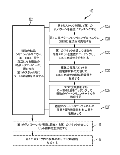
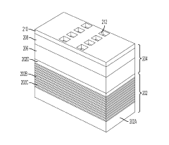
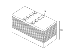
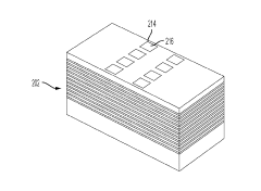
Three-dimensional dynamic random access memory (3D DRAM) gate-all-around (GAA) design using stacked SI/SIGE
PatentActiveJP2024516386A
Innovation
- A method for forming a 3D DRAM structure using alternating crystalline silicon and silicon germanium layers, with etching and filling processes to create a gate-all-around (GAA) design, including vertical word lines, horizontal bit lines, and capacitor features, enabling scalable memory densities.
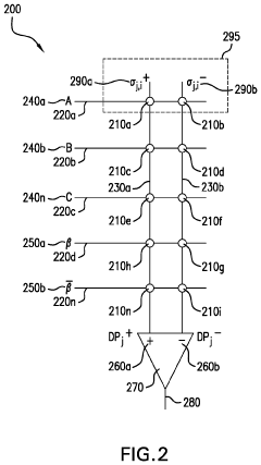
Analog neuromoprhic circuit with stacks of resistive memory crossbar configurations
PatentPendingUS20230028592A1
Innovation
- An analog neuromorphic circuit implementing a three-dimensional stack of resistive memory crossbar configurations, which allows for simultaneous execution of multiple operations through input and output selectors and activation functions, reducing the need for extensive physical space and power consumption.
Thermal Management Challenges
Thermal management represents one of the most critical challenges in 3D stacking of memory and logic using Gate-All-Around (GAA) transistors for Neuromorphic System-on-Chips (SoCs). The vertical integration of multiple dies significantly increases power density, creating thermal hotspots that can severely impact system reliability and performance. In traditional 2D architectures, heat dissipation occurs primarily through the silicon substrate and package, but 3D stacking introduces additional thermal resistance between layers, impeding efficient heat transfer.
The power density in 3D stacked neuromorphic systems can exceed 100W/cm², particularly at logic layers where computational elements are concentrated. This creates vertical thermal gradients that may reach 20-30°C between adjacent layers. Such temperature differentials induce mechanical stress due to coefficient of thermal expansion mismatches, potentially leading to microcracks, delamination, and premature failure of Through-Silicon Vias (TSVs) that provide vertical interconnections.
GAA transistor architecture, while offering superior electrostatic control and reduced leakage current compared to FinFET technology, introduces unique thermal considerations. The wrapped gate structure limits the thermal conduction paths from the channel region, concentrating heat in smaller volumes. Preliminary studies indicate that GAA transistors in 3D stacked configurations may experience 15-20% higher peak temperatures than equivalent FinFET implementations under identical workloads.
Neuromorphic computing workloads present additional thermal management complexities due to their spatiotemporal dynamics. Unlike conventional processors with relatively predictable thermal profiles, neuromorphic systems exhibit highly variable thermal patterns based on neural network activity. This dynamic thermal behavior complicates the design of effective cooling solutions and thermal management strategies.
Current approaches to address these challenges include the integration of microfluidic cooling channels between dies, the strategic placement of thermal Through-Silicon Vias (tTSVs), and the development of thermally-aware neuromorphic algorithms. Microfluidic cooling has demonstrated the potential to reduce peak temperatures by up to 35°C in laboratory settings, though integration challenges remain significant. Thermal TSVs, while less effective than active cooling, offer manufacturing compatibility advantages and can reduce thermal resistance by 20-30% when optimally distributed.
Advanced thermal simulation tools have become essential for predicting hotspot formation in 3D neuromorphic architectures. These tools must account for the complex interaction between electrical, thermal, and mechanical domains across multiple stacked layers. Recent developments in electrothermal co-simulation capabilities have improved prediction accuracy by 40-50% compared to decoupled approaches, enabling more effective thermal management strategies during the design phase.
Manufacturing Yield Considerations
Manufacturing yield represents a critical challenge in the implementation of 3D stacking technologies for neuromorphic SoCs using Gate-All-Around (GAA) transistors. The vertical integration of memory and logic components introduces multiple yield-impacting factors that must be carefully managed to ensure economic viability of these advanced systems.
The yield considerations for 3D stacked neuromorphic architectures can be categorized into three primary domains: die-level defects, bonding interface issues, and thermal-induced failures. At the die level, the GAA transistor fabrication process introduces unique yield challenges due to its complex three-dimensional channel structure. The suspended nanowire or nanosheet channels require precise etching processes that can lead to variability in channel dimensions, potentially affecting device performance uniformity across the wafer.
Bonding interface defects represent another significant yield concern. The Through-Silicon Via (TSV) connections between memory and logic layers must maintain extremely high reliability standards, as a single failed connection can render an entire functional block inoperable. Current manufacturing processes typically achieve TSV yields of 99.9%, but neuromorphic applications may require even higher reliability due to their massively parallel architecture.
Thermal considerations during manufacturing also impact yield significantly. The different thermal expansion coefficients of materials used in the 3D stack can create mechanical stress during high-temperature processing steps, potentially leading to wafer warpage, delamination, or microcracks. These defects may not be immediately detectable but can manifest as reliability issues during operation.
Statistical yield modeling for these complex structures requires new approaches that account for the interdependencies between layers. Traditional yield models based on critical area analysis must be extended to incorporate vertical integration effects. Recent research indicates that for neuromorphic applications, the yield of memory layers typically dominates the overall system yield due to their larger area and higher density compared to logic components.
Cost-effective testing strategies represent another manufacturing yield challenge. Known-good-die (KGD) testing before stacking is essential but increases manufacturing complexity. For neuromorphic systems, which may contain thousands of neural processing elements, developing efficient test patterns that can identify defective components without exhaustive testing remains an active research area.
Recent advances in yield enhancement techniques include redundancy schemes specifically designed for neuromorphic architectures, where the inherent fault tolerance of neural networks can be leveraged to accommodate certain types of manufacturing defects. Additionally, design-for-yield methodologies that optimize the physical layout of 3D stacked components based on statistical defect distributions have shown promise in improving overall manufacturing yields.
Unlock deeper insights with Patsnap Eureka Quick Research — get a full tech report to explore trends and direct your research. Try now!
Generate Your Research Report Instantly with AI Agent
Supercharge your innovation with Patsnap Eureka AI Agent Platform!