

RRAM Crossbar Arrays for Implementing Synaptic Cores.
SEP 10, 20259 MIN READ
Generate Your Research Report Instantly with AI Agent
Patsnap Eureka helps you evaluate technical feasibility & market potential.
RRAM Crossbar Technology Evolution and Objectives
Resistive Random Access Memory (RRAM) technology has evolved significantly over the past two decades, transitioning from theoretical concepts to practical implementations in neuromorphic computing systems. The journey began in the early 2000s with fundamental research on resistive switching phenomena in metal oxides, which demonstrated the potential for non-volatile memory applications. By 2010, researchers had successfully fabricated simple RRAM cells, establishing the foundation for more complex architectures.
The mid-2010s marked a pivotal advancement with the development of crossbar array structures, which enabled higher density memory configurations and parallel operations. This architectural breakthrough addressed scaling limitations of conventional memory technologies while offering unique advantages for neural network implementations. The inherent physical properties of RRAM devices—particularly their ability to maintain multiple resistance states—naturally aligned with the requirements for implementing artificial synapses.
Recent technological evolution has focused on improving device reliability, reducing variability, and enhancing endurance characteristics. Material engineering innovations have introduced complex metal oxides and novel electrode materials that significantly improve switching characteristics and retention properties. Fabrication techniques have also evolved to enable integration with CMOS processes, facilitating hybrid neuromorphic systems that combine the computational efficiency of RRAM-based synaptic cores with traditional digital processing.
The primary objective of RRAM crossbar technology for synaptic cores is to achieve efficient hardware implementation of artificial neural networks with significantly reduced power consumption compared to conventional computing architectures. This aligns with the growing demand for edge AI applications where energy efficiency is paramount. Additionally, the technology aims to overcome the von Neumann bottleneck by enabling in-memory computing paradigms where data processing occurs directly within the memory array.
Another critical objective is scaling synaptic density to support increasingly complex neural network models. Current research targets achieving arrays with dimensions exceeding 1024×1024 elements while maintaining acceptable yield and performance characteristics. This would enable the implementation of practical neural network accelerators capable of supporting modern deep learning architectures.
Looking forward, the technology roadmap emphasizes achieving precise multi-level cell capabilities to represent synaptic weights with higher resolution, thereby improving neural network accuracy. Researchers are also exploring three-dimensional integration techniques to further increase synaptic density and computational throughput. The ultimate goal remains developing a mature technology platform that can serve as the foundation for commercial neuromorphic computing systems with orders of magnitude better energy efficiency than current solutions.
Neuromorphic Computing Market Analysis
The neuromorphic computing market is experiencing significant growth, driven by the increasing demand for AI applications and the limitations of traditional computing architectures. Current market valuations place the global neuromorphic computing sector at approximately $3.2 billion in 2023, with projections indicating a compound annual growth rate (CAGR) of 24.7% through 2030, potentially reaching $19.8 billion by the end of the decade.
The integration of RRAM crossbar arrays for implementing synaptic cores represents a critical technological advancement within this market. These arrays offer substantial advantages in terms of power efficiency, with energy consumption reductions of up to 100x compared to conventional CMOS-based neural networks, making them particularly attractive for edge computing applications where power constraints are significant.
Market segmentation reveals diverse application areas for neuromorphic systems utilizing RRAM-based synaptic cores. The automotive sector currently accounts for approximately 18% of market demand, primarily for advanced driver assistance systems and autonomous vehicle development. Healthcare applications represent 15% of the market, with significant growth potential in medical imaging and diagnostic systems. Consumer electronics maintains the largest share at 27%, driven by smartphone AI processors and smart home devices.
Geographically, North America leads the market with a 42% share, bolstered by substantial research investments and the presence of key technology developers. Asia-Pacific represents the fastest-growing region with a 29% annual growth rate, fueled by aggressive semiconductor manufacturing expansion in countries like China, South Korea, and Taiwan.
The demand for RRAM-based neuromorphic solutions is being accelerated by several market factors. Data center operators are increasingly seeking energy-efficient AI processing solutions, with potential energy savings of 60-80% compared to GPU-based systems. Edge computing requirements are expanding at 34% annually, creating opportunities for low-power neuromorphic processors in IoT applications.
Key market challenges include the relatively high initial manufacturing costs of RRAM crossbar arrays, with production expenses currently 2.5x higher than conventional memory technologies. Additionally, software ecosystem limitations restrict broader adoption, as programming frameworks for neuromorphic systems remain specialized and fragmented.
Industry analysts predict that the RRAM-based synaptic core segment will grow at 31% annually through 2028, outpacing the broader neuromorphic computing market. This growth is supported by increasing venture capital investment, which reached $1.2 billion in 2022 specifically for neuromorphic hardware startups, representing a 45% increase from the previous year.
RRAM Synaptic Core Implementation Challenges
The implementation of RRAM crossbar arrays as synaptic cores faces several significant technical challenges that must be addressed to achieve practical neuromorphic computing systems. Device variability represents one of the most critical issues, as RRAM cells exhibit considerable variations in resistance states, switching voltages, and endurance characteristics. These variations stem from manufacturing process inconsistencies, material defects, and inherent stochastic switching mechanisms, resulting in unpredictable weight values that compromise neural network accuracy.
Sneak path currents present another major obstacle in crossbar architectures. When reading a specific cell, unintended current paths through neighboring cells can distort the measured resistance value, leading to erroneous weight interpretations. This issue becomes increasingly severe as array sizes scale up, limiting the practical dimensions of RRAM crossbar arrays without additional circuit components.
The non-linear I-V characteristics of RRAM devices further complicate their implementation as ideal synaptic elements. While neural network models typically assume linear weight operations, RRAM devices exhibit threshold-based switching and non-linear conduction behaviors. This discrepancy necessitates complex compensation schemes or modified training algorithms to maintain computational accuracy.
Limited endurance poses a significant constraint for practical deployment. RRAM devices typically withstand 10^6 to 10^9 write cycles before failure, which may be insufficient for continuous learning applications requiring frequent weight updates. This limitation is particularly problematic for online learning scenarios where synaptic weights undergo constant modification.
Power consumption during programming operations remains substantially higher than biological synapses. The high voltages required for reliable switching (typically 1-3V) result in significant energy expenditure during weight updates, undermining the energy efficiency advantages that neuromorphic computing promises to deliver.
Retention stability presents challenges for long-term information storage. RRAM resistance states can drift over time due to thermal effects and internal atomic rearrangements, causing gradual degradation of stored weight values. This drift necessitates periodic refreshing or error correction mechanisms that add complexity to the system architecture.
Integration with CMOS peripherals introduces additional design complexities. The interface between RRAM arrays and conventional CMOS circuitry requires specialized drivers, sense amplifiers, and control logic that must operate at compatible voltage levels while maintaining precise current control. This integration challenge often results in significant overhead that diminishes the density advantages of RRAM technology.
Current RRAM Crossbar Array Architectures
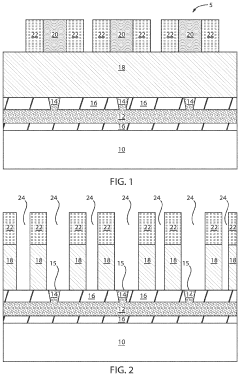
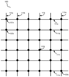
01 RRAM crossbar architecture for neuromorphic computing
Resistive Random Access Memory (RRAM) crossbar arrays can be configured as synaptic cores for neuromorphic computing applications. These architectures mimic the functionality of biological neural networks by using resistive memory elements at crosspoints to represent synaptic weights. The crossbar structure allows for efficient parallel processing and matrix operations essential for neural network computations, enabling high-density integration and energy-efficient implementation of artificial neural networks.- RRAM crossbar array architecture for neuromorphic computing: Resistive Random Access Memory (RRAM) crossbar arrays can be configured as synaptic cores for neuromorphic computing systems. These architectures enable efficient implementation of neural networks by mimicking biological synapses through resistive switching elements at crosspoints. The crossbar structure allows for parallel processing and high-density integration, making it ideal for artificial intelligence applications requiring low power consumption and high computational efficiency.
- Synaptic weight programming and update mechanisms: Various techniques for programming and updating synaptic weights in RRAM crossbar arrays have been developed. These include pulse-based programming methods, multi-level cell configurations, and specialized circuits for implementing learning algorithms. These mechanisms enable the implementation of synaptic plasticity, allowing the neuromorphic systems to learn and adapt through weight modifications based on input patterns and training algorithms.
- Integration of RRAM with CMOS technology: The integration of RRAM crossbar arrays with complementary metal-oxide-semiconductor (CMOS) technology enables the creation of complete neuromorphic computing systems. This hybrid approach combines the high-density storage capabilities of RRAM with the signal processing capabilities of CMOS circuits. The integration techniques include back-end-of-line processing, 3D stacking, and monolithic integration, allowing for compact and efficient synaptic core implementations.
- Novel materials and device structures for RRAM synaptic elements: Advanced materials and innovative device structures have been developed to enhance the performance of RRAM-based synaptic elements. These include various oxide materials, filamentary switching mechanisms, and interface engineering techniques that improve reliability, endurance, and multi-level storage capabilities. These innovations enable more accurate emulation of biological synapses and enhance the overall performance of neuromorphic computing systems.
- System-level architectures and applications: Complete system architectures incorporating RRAM crossbar arrays as synaptic cores have been designed for various applications. These systems include specialized peripheral circuits for signal conditioning, analog-to-digital conversion, and control logic. Applications range from pattern recognition and image processing to autonomous systems and edge computing devices. The architectures are optimized for energy efficiency, throughput, and adaptability to different neural network models.
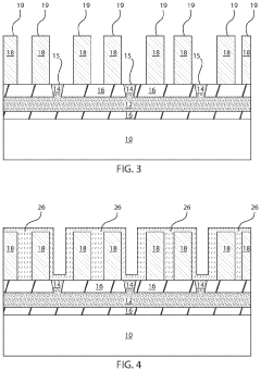
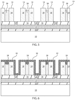
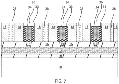
02 Fabrication techniques for RRAM synaptic arrays
Advanced fabrication methods for RRAM crossbar arrays involve integrating resistive switching materials with CMOS technology. These techniques include deposition of specialized oxide layers, precise patterning of nanoscale crossbar structures, and 3D stacking to increase density. The manufacturing processes focus on ensuring uniformity of resistive elements across the array, minimizing variability, and enhancing reliability for consistent synaptic behavior in neuromorphic applications.Expand Specific Solutions03 Programming and weight update mechanisms
RRAM synaptic cores require sophisticated programming algorithms to precisely control the conductance states of memory cells. These mechanisms include pulse-based programming schemes, adaptive weight update protocols, and feedback systems to compensate for device variability. The programming techniques enable multi-level resistance states in each cell, allowing for analog-like weight representation crucial for implementing learning algorithms and synaptic plasticity in hardware neural networks.Expand Specific Solutions04 Integration with peripheral circuits and systems
RRAM crossbar arrays are integrated with peripheral circuits including sensing amplifiers, driver circuits, and control logic to form complete synaptic core systems. These supporting circuits manage read/write operations, address decoding, and signal conditioning. The integration approaches focus on minimizing area overhead while maintaining signal integrity, addressing sneak path issues in crossbar structures, and enabling efficient communication between the synaptic core and other components of neuromorphic systems.Expand Specific Solutions05 Novel materials and device structures
Research on advanced materials and innovative device structures aims to enhance the performance of RRAM-based synaptic cores. These developments include exploration of various switching materials like metal oxides, chalcogenides, and 2D materials, as well as novel device architectures such as vertical RRAMs and selector-less arrays. These innovations address challenges related to endurance, retention, power consumption, and switching speed, which are critical for implementing efficient neuromorphic computing systems.Expand Specific Solutions
Leading Companies in RRAM and Neuromorphic Hardware
RRAM Crossbar Arrays for Implementing Synaptic Cores technology is currently in the early growth phase, characterized by increasing research activity and commercial interest. The market for neuromorphic computing solutions using RRAM technology is projected to expand significantly, driven by AI applications requiring energy-efficient edge computing. While technical challenges remain, major players like IBM, Huawei, and Qualcomm are advancing the technology alongside specialized startups like TetraMem. Academic institutions, particularly in China (Huazhong University, Zhejiang University) and Singapore (NTU, NUS), are collaborating with industry partners to overcome integration challenges, improve reliability, and scale manufacturing processes for commercial viability.
TetraMem, Inc.
Technical Solution: TetraMem has developed a proprietary RRAM crossbar array technology specifically designed for neuromorphic computing applications. Their solution implements synaptic cores using analog computing principles within the memory array itself, enabling true in-memory computing. TetraMem's architecture features multi-bit RRAM cells that can store multiple weight values per cell, significantly increasing the synaptic density compared to conventional approaches. Their technology employs a unique programming algorithm that addresses the non-linearity and variability issues common in RRAM devices, achieving higher precision for neural network operations. The company has demonstrated synaptic cores with thousands of connections per neuron, with their crossbar arrays showing excellent retention characteristics and endurance exceeding 10^6 cycles[1]. TetraMem's implementation includes peripheral circuitry optimized for parallel vector-matrix multiplication operations, which are fundamental to neural network inference.
Strengths: High integration density allowing more synaptic connections in smaller area; lower power consumption through in-memory computing; multi-bit capability increasing effective storage density. Weaknesses: Requires specialized programming schemes to overcome RRAM variability; may face challenges with thermal stability in high-density arrays; custom design requires specialized software tools for neural network mapping.
International Business Machines Corp.
Technical Solution: IBM has pioneered advanced RRAM crossbar array technology for neuromorphic computing through their Phase-Change Memory (PCM) based synaptic cores. Their implementation features multi-level cell capability, allowing each RRAM element to store multiple weight values with analog precision. IBM's architecture incorporates sophisticated peripheral circuitry for precise programming and reading operations, addressing the inherent variability of resistive memory elements. Their crossbar arrays have been demonstrated at scales of 256×256 and beyond, with impressive density metrics of >10^7 synapses per square centimeter[2]. IBM's synaptic cores include on-chip learning capabilities through specialized programming circuits that can implement various learning algorithms including spike-timing-dependent plasticity (STDP). The company has demonstrated successful integration of these RRAM-based synaptic cores with CMOS neurons to create complete neuromorphic systems capable of pattern recognition and classification tasks with significantly reduced power consumption compared to conventional digital implementations[3].
Strengths: Industry-leading research infrastructure allowing comprehensive material and device optimization; extensive experience integrating novel memory with CMOS technology; demonstrated large-scale neuromorphic systems with on-chip learning. Weaknesses: Complex fabrication processes may increase manufacturing costs; requires precise control of resistance states for reliable neural network operation; potential endurance limitations for intensive learning applications.
Key Patents in RRAM Synaptic Core Technology
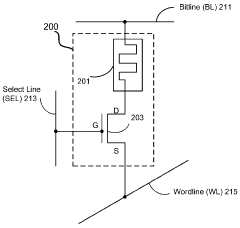
RRAM cells in crossbar array architecture
PatentActiveUS20200066798A1
Innovation
- The method involves forming vertical crossbar RRAM cells by creating a U-shaped bottom electrode shared between neighboring cells, using self-aligning techniques to integrate high-density RRAMs without reactive etching, allowing for vertical alignment and isolation of active areas, thus enabling a crossbar structure with one word line and two bit lines.
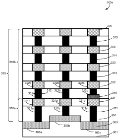
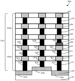
CMOS-compatible resistive random-access memory devices with a via device structure
PatentWO2024073681A1
Innovation
- The implementation of a via device structure for RRAM devices, where a switching oxide layer is fabricated within vias in an etch stop layer, allowing for reduced critical device size defined by the via opening size rather than the electrode wire dimensions, and the use of etch stop layers for high etching selectivity and oxygen barrier protection.
Energy Efficiency Analysis of RRAM Synaptic Cores
Energy efficiency is a critical factor in the practical implementation of RRAM-based synaptic cores for neuromorphic computing systems. Current analyses indicate that RRAM crossbar arrays offer significant energy advantages compared to conventional CMOS-based neural network implementations, with potential energy savings of up to 10-100x depending on the specific architecture and application.
The energy consumption in RRAM synaptic cores can be categorized into three main components: read operations, write operations, and peripheral circuit overhead. Read operations typically consume 10-100 pJ per synaptic operation, while write operations are more energy-intensive, requiring 100-1000 pJ per weight update. The energy efficiency advantage of RRAM becomes particularly pronounced in inference tasks where read operations dominate.
Recent benchmarking studies have demonstrated that 1T1R (one-transistor-one-resistor) RRAM crossbar arrays can achieve energy efficiencies of approximately 10 TOPS/W (Tera Operations Per Second per Watt) for matrix-vector multiplication operations. This represents a substantial improvement over GPU implementations which typically achieve 1-5 TOPS/W for similar neural network operations.
The energy efficiency of RRAM synaptic cores is heavily influenced by device characteristics such as on/off resistance ratio, switching voltage, and device variability. Higher on/off ratios enable more distinct resistance states but often require higher programming voltages, creating an energy-performance tradeoff. Devices with on/off ratios exceeding 10³ while maintaining sub-3V programming voltages represent the current sweet spot for energy-efficient operation.
Array-level considerations also significantly impact energy efficiency. Sneak path currents in passive crossbar arrays can lead to substantial energy waste, while 1T1R configurations mitigate this issue at the cost of increased area overhead. Recent innovations in selector devices have enabled quasi-passive arrays that approach the energy efficiency of 1T1R configurations while maintaining higher density.
Peripheral circuitry, including sense amplifiers, write drivers, and analog-to-digital converters, contributes significantly to the overall energy budget. In many implementations, these components can consume more than 50% of the total energy. Advanced circuit techniques such as time-domain sensing and in-memory computing architectures are being developed to reduce this overhead.
Looking forward, emerging techniques such as multi-level cell programming, spike-based computing paradigms, and advanced material engineering promise to further improve the energy efficiency of RRAM synaptic cores by 1-2 orders of magnitude in the next generation of devices, potentially enabling sub-pJ per operation energy consumption for neuromorphic computing applications.
Fabrication Processes and Materials Science Considerations
The fabrication of RRAM (Resistive Random Access Memory) crossbar arrays for synaptic cores requires sophisticated processes that balance precision, scalability, and material compatibility. Current fabrication approaches primarily utilize CMOS-compatible processes, enabling integration with existing semiconductor manufacturing infrastructure. The standard process flow includes substrate preparation, bottom electrode deposition, resistive switching layer formation, top electrode patterning, and encapsulation.
Material selection represents a critical consideration in RRAM fabrication. Metal oxides such as HfOx, TaOx, and TiOx have emerged as leading candidates for the resistive switching layer due to their favorable switching characteristics and compatibility with standard semiconductor processes. The electrode materials—typically noble metals like Pt, Au, or more CMOS-compatible options such as TiN and W—significantly influence device performance through their work function and interface properties with the switching layer.
Interface engineering between electrodes and the switching layer has proven crucial for optimizing device reliability and performance. Techniques such as atomic layer deposition (ALD) enable precise control of layer thickness down to sub-nanometer precision, while reactive sputtering offers higher throughput for industrial applications. The introduction of interfacial layers or dopants can effectively modulate switching behavior and reduce variability across devices.
Scaling challenges become particularly pronounced as dimensions approach sub-10nm nodes. At these scales, material defects and process variations exert outsized influence on device characteristics. Advanced lithography techniques including e-beam lithography and nanoimprint lithography have been employed to achieve the necessary feature sizes, though throughput limitations remain a concern for mass production.
Device-to-device variability presents perhaps the most significant challenge for neuromorphic applications. This variability stems from stochastic filament formation processes and material inhomogeneities. Recent research has focused on developing self-limiting current compliance mechanisms and engineered switching layers with more deterministic behavior. Atomic-scale characterization techniques such as transmission electron microscopy (TEM) and atom probe tomography have provided crucial insights into filament formation dynamics.
Post-fabrication treatments including thermal annealing and electrical forming processes significantly impact device performance. These treatments help stabilize the microstructure and establish initial conduction pathways. Emerging approaches incorporate novel materials such as 2D materials and complex oxides to achieve multi-level resistance states necessary for efficient synaptic weight implementation.
Unlock deeper insights with Patsnap Eureka Quick Research — get a full tech report to explore trends and direct your research. Try now!
Generate Your Research Report Instantly with AI Agent
Supercharge your innovation with Patsnap Eureka AI Agent Platform!