

Advanced Patterning Methods For High Yield SOT MRAM Arrays
AUG 28, 20259 MIN READ
Generate Your Research Report Instantly with AI Agent
PatSnap Eureka helps you evaluate technical feasibility & market potential.
SOT MRAM Technology Background and Objectives
Spin-Orbit Torque Magnetoresistive Random Access Memory (SOT-MRAM) has emerged as a promising next-generation non-volatile memory technology, offering significant advantages over conventional memory solutions. The evolution of SOT-MRAM technology can be traced back to the discovery of spin-transfer torque (STT) effects in the early 2000s, which laid the foundation for spintronic memory devices. SOT-MRAM represents a further advancement in this field, leveraging spin-orbit coupling phenomena to achieve more efficient switching mechanisms.
The technological trajectory of SOT-MRAM has been characterized by continuous improvements in materials science, device architecture, and fabrication techniques. Initial research focused primarily on fundamental physics of spin-orbit interactions, gradually transitioning to practical device implementations. Recent years have witnessed accelerated development in SOT-MRAM, driven by increasing demands for energy-efficient, high-speed, and reliable memory solutions for various computing applications.
The primary technical objectives for advanced patterning methods in SOT-MRAM arrays center around achieving high yield manufacturing processes while maintaining device performance. Specifically, these objectives include developing precise etching techniques capable of defining nanoscale magnetic tunnel junctions (MTJs) with minimal structural damage, establishing reliable methods for integrating SOT channel materials with conventional CMOS processes, and creating uniform arrays with consistent electrical and magnetic properties across the entire wafer.
Current trends in SOT-MRAM technology development indicate a growing emphasis on scalability to sub-20nm dimensions, which necessitates increasingly sophisticated patterning approaches. The industry is moving toward multi-layer patterning strategies that can accommodate the complex stack structures inherent to SOT-MRAM devices while preserving the integrity of sensitive magnetic materials.
Another significant trend is the exploration of novel materials for both the SOT channel and magnetic layers, which introduces additional challenges for patterning processes. These materials must be compatible with existing semiconductor manufacturing infrastructure while delivering enhanced performance metrics such as lower switching current, faster writing speed, and improved thermal stability.
The ultimate goal of advanced patterning methods for SOT-MRAM is to enable mass production of high-density memory arrays with yields comparable to established memory technologies. This requires overcoming several technical hurdles, including edge damage control during etching, precise alignment between multiple layers, and prevention of material intermixing at interfaces. Success in these areas would position SOT-MRAM as a viable candidate for replacing conventional memory in various applications, from embedded cache memory to storage-class memory solutions.
Market Analysis for SOT MRAM Applications
The SOT-MRAM (Spin-Orbit Torque Magnetoresistive Random Access Memory) market is experiencing significant growth potential as the technology addresses critical limitations of conventional memory solutions. Current market projections indicate that the overall MRAM market is expected to reach $5.3 billion by 2028, with SOT-MRAM positioned to capture an increasing share due to its superior performance characteristics.
The primary market segments for SOT-MRAM applications include data centers, automotive electronics, industrial automation, aerospace, and consumer electronics. Data centers represent the largest potential market, driven by increasing demands for energy-efficient, high-speed, and non-volatile memory solutions that can reduce power consumption while maintaining performance. The automotive sector follows closely, with requirements for reliable memory technologies capable of withstanding extreme operating conditions.
Industry analysis reveals that SOT-MRAM's unique value proposition centers on its unlimited endurance, fast switching speeds (sub-nanosecond), and lower power consumption compared to conventional STT-MRAM. These advantages position SOT-MRAM as an ideal candidate for cache memory, replacing SRAM in various computing architectures, and as persistent memory for data-intensive applications.
Market adoption trends indicate that SOT-MRAM is currently transitioning from research to commercialization, with early adopters primarily in high-performance computing and mission-critical systems. The technology's radiation hardness makes it particularly attractive for aerospace and defense applications, where market penetration is expected to occur first.
Competitive analysis shows that major semiconductor manufacturers including Samsung, Intel, TSMC, and specialized memory producers like Everspin Technologies are investing heavily in SOT-MRAM development. This competitive landscape suggests market consolidation may occur as the technology matures, with intellectual property becoming a key differentiator.
Economic factors influencing market growth include decreasing production costs as manufacturing processes mature and increasing demand for edge computing solutions that require low-power, high-performance memory. The total addressable market for SOT-MRAM is expanding as applications in IoT devices and AI accelerators create new opportunities.
Regional market analysis indicates that Asia-Pacific, particularly Taiwan, South Korea, and Japan, leads in SOT-MRAM manufacturing capacity, while North America dominates in research and intellectual property development. Europe is emerging as a significant market for automotive and industrial applications of SOT-MRAM technology.
Customer requirements analysis shows growing demand for memory solutions that combine the speed of SRAM, the density of DRAM, and the non-volatility of flash memory—a combination that SOT-MRAM is uniquely positioned to deliver. This convergence of performance characteristics is expected to drive adoption across multiple sectors once high-yield manufacturing processes are established.
Current Challenges in SOT MRAM Patterning
Spin-orbit torque magnetic random access memory (SOT-MRAM) represents a promising next-generation non-volatile memory technology, offering advantages in speed, endurance, and power consumption. However, the fabrication of high-yield SOT-MRAM arrays faces significant patterning challenges that currently limit commercial viability and widespread adoption.
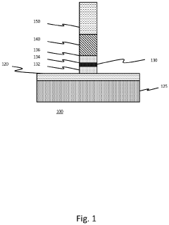
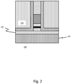
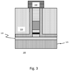
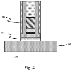
The primary challenge in SOT-MRAM patterning stems from the complex multilayer stack structure, typically consisting of magnetic tunnel junctions (MTJs) with multiple ultrathin layers including ferromagnetic materials, tunnel barriers, and heavy metal layers. These stacks require precise etching with nanometer-scale accuracy while maintaining the integrity of magnetic properties, which conventional etching techniques struggle to achieve.
Ion beam etching (IBE), the current industry standard for MTJ patterning, presents several limitations when applied to SOT-MRAM structures. The physical nature of IBE causes material redeposition on sidewalls, creating potential shorting paths between the top and bottom electrodes. This issue becomes more pronounced as device dimensions shrink below 30nm, where edge effects dominate device performance.
Another critical challenge is the precise patterning of the heavy metal layer that generates the spin-orbit torque. This layer must maintain excellent interface quality with the adjacent ferromagnetic layer while achieving the desired dimensions. Any degradation at this interface significantly reduces the spin-orbit coupling efficiency and consequently diminishes the writing performance of the device.
Pattern transfer fidelity represents a substantial hurdle, particularly for high-density arrays. The extreme aspect ratios required for SOT-MRAM cells create difficulties in maintaining consistent critical dimensions across large arrays. Variations in pattern dimensions lead to device-to-device performance inconsistencies, reducing overall yield and reliability.
Material damage during patterning processes constitutes another significant challenge. Conventional etching techniques can induce crystallographic damage and alter the magnetic properties of functional layers. This is particularly problematic for the free layer, where maintaining precise magnetic anisotropy is essential for proper device operation.
Edge roughness control has emerged as a critical factor affecting device performance. Rough edges create localized demagnetization fields that can destabilize the magnetic state and increase switching current requirements. Current patterning methods struggle to achieve the sub-nanometer edge roughness control needed for optimal device performance.
The integration of SOT-MRAM with CMOS backend processes presents additional challenges. The thermal budget constraints of CMOS backend processing limit the available patterning and annealing options, requiring development of low-temperature processes that maintain material properties while achieving high pattern fidelity.
Advanced Patterning Solutions for SOT MRAM
01 SOT-MRAM array structure optimization
Optimizing the structure of Spin-Orbit Torque Magnetic Random Access Memory (SOT-MRAM) arrays is crucial for achieving high yield. This includes designing efficient memory cell layouts, optimizing the arrangement of bit lines and word lines, and implementing proper isolation between adjacent cells. These structural improvements help reduce interference between cells and enhance the overall performance and reliability of the memory array.- SOT-MRAM array structure optimization: Optimizing the structure of Spin-Orbit Torque Magnetic Random Access Memory (SOT-MRAM) arrays is crucial for achieving high yield. This includes designing efficient cell layouts, optimizing bit line and word line configurations, and implementing proper isolation between memory cells. Advanced array architectures can minimize interference between adjacent cells and reduce defect sensitivity, leading to improved manufacturing yield and device performance.
- Material selection and deposition techniques: The selection of appropriate materials and deposition techniques significantly impacts SOT-MRAM array yield. High-quality magnetic materials with optimized properties, precise control of layer thicknesses, and uniform deposition processes are essential. Advanced deposition methods such as physical vapor deposition (PVD), atomic layer deposition (ALD), and sputtering techniques with optimized parameters help ensure consistent material properties across the array, reducing defects and improving yield.
- Process control and defect reduction strategies: Implementing robust process control and defect reduction strategies is essential for high-yield SOT-MRAM arrays. This includes advanced lithography techniques, precise etching processes, and contamination control measures. In-line monitoring, statistical process control, and defect inspection tools help identify and address yield-limiting factors. Post-fabrication treatments and annealing processes can also be optimized to repair defects and improve device characteristics.
- Circuit design and peripheral components: Innovative circuit design and peripheral components play a crucial role in achieving high-yield SOT-MRAM arrays. This includes designing robust sense amplifiers, write drivers, and addressing circuits that can tolerate process variations. Implementing error correction codes (ECC), redundancy schemes, and repair mechanisms can significantly improve effective yield by compensating for defective cells. Advanced read/write schemes that minimize disturb effects also contribute to higher manufacturing yield.
- Testing and reliability enhancement techniques: Comprehensive testing and reliability enhancement techniques are vital for ensuring high-yield SOT-MRAM arrays. This includes developing specialized test patterns, burn-in procedures, and accelerated lifetime testing methodologies. Implementing built-in self-test (BIST) circuits, on-chip monitoring, and adaptive biasing schemes can identify and mitigate reliability issues. Advanced failure analysis techniques help understand yield-limiting mechanisms, enabling continuous process improvement and reliability enhancement.
02 Material selection and deposition techniques
The choice of materials and deposition methods significantly impacts the yield of SOT-MRAM arrays. Using high-quality magnetic materials with appropriate magnetic properties, optimizing the thickness and composition of the free layer and reference layer, and employing precise deposition techniques such as sputtering or atomic layer deposition can improve uniformity across the array and enhance device performance.Expand Specific Solutions03 Process control and manufacturing optimization
Strict process control during manufacturing is essential for high-yield SOT-MRAM arrays. This includes optimizing etching processes to prevent damage to magnetic layers, implementing precise lithography techniques for accurate pattern definition, controlling thermal budgets during integration, and developing robust testing methodologies to identify and mitigate defects early in the production process.Expand Specific Solutions04 Integration with CMOS technology
Successful integration of SOT-MRAM with complementary metal-oxide-semiconductor (CMOS) technology is critical for high-yield manufacturing. This involves developing compatible fabrication processes, optimizing the interface between MRAM cells and CMOS circuitry, implementing effective isolation techniques to prevent interference, and designing appropriate sensing circuits that can reliably read the magnetic state of memory cells.Expand Specific Solutions05 Advanced switching mechanisms and reliability enhancement
Implementing advanced switching mechanisms can significantly improve the yield and reliability of SOT-MRAM arrays. This includes optimizing the spin-orbit torque effect for efficient switching, developing techniques to reduce write errors, implementing error correction codes, enhancing thermal stability of magnetic elements, and designing circuits that can compensate for process variations across the array.Expand Specific Solutions
Leading Companies in SOT MRAM Development
The SOT MRAM array patterning technology market is currently in its early growth phase, characterized by significant R&D investments but limited commercial deployment. The global MRAM market is projected to reach approximately $5 billion by 2028, with SOT MRAM representing an emerging segment. Technologically, major semiconductor players are at different maturity levels: IBM, Samsung, and TSMC lead with advanced research publications and patents, while companies like QUALCOMM and Micron are actively developing integration capabilities. Specialized entities like ANTAIOS and Shanghai Ciyu are focusing exclusively on SOT MRAM commercialization. Academic-industrial partnerships involving CNRS, Université Paris-Saclay, and IMEC are accelerating technological breakthroughs. Equipment manufacturers including Applied Materials and Tokyo Electron are developing specialized patterning tools to address the unique fabrication challenges of high-yield SOT MRAM arrays.
International Business Machines Corp.
Technical Solution: IBM has developed advanced patterning techniques specifically for SOT-MRAM arrays that combine extreme ultraviolet (EUV) lithography with directed self-assembly (DSA) processes. Their approach utilizes a hybrid lithography scheme where EUV defines critical dimensions while DSA enhances pattern fidelity and reduces edge roughness. IBM's technique incorporates multi-layer patterning with precise alignment control systems that maintain sub-5nm overlay accuracy between the SOT and magnetic layers. They've implemented specialized etch processes with high selectivity to minimize damage to magnetic materials during fabrication. Additionally, IBM has developed unique planarization methods that ensure uniform electrical characteristics across the array, employing chemical mechanical polishing (CMP) techniques optimized specifically for SOT-MRAM structures. Their process includes in-line metrology systems for real-time monitoring of critical dimensions and magnetic properties to maintain high yield rates across 300mm wafers[1][3].
Strengths: Superior integration with CMOS processes allowing for seamless incorporation into existing semiconductor manufacturing lines. Exceptional pattern fidelity at sub-10nm dimensions. Weaknesses: Higher manufacturing costs due to EUV lithography requirements and complex multi-step processes. Limited scalability below certain dimensions due to fundamental magnetic material constraints.
Samsung Electronics Co., Ltd.
Technical Solution: Samsung has pioneered a comprehensive patterning approach for SOT-MRAM arrays focusing on high-density integration and yield optimization. Their technology employs a multi-layer deposition and patterning sequence with precise control of magnetic stack interfaces. Samsung utilizes advanced 193nm immersion lithography combined with multiple patterning techniques to achieve critical dimensions below 20nm for SOT channel structures. Their process incorporates specialized sidewall spacer technology to define ultra-narrow SOT channels while maintaining consistent electrical properties. Samsung has developed proprietary etching recipes that preserve magnetic layer integrity during patterning, utilizing low-energy ion beam etching with specialized gas chemistries. Additionally, they've implemented advanced inspection and metrology systems including in-line magnetic testing to identify defects early in the manufacturing process. Samsung's approach includes thermal budget management throughout the process flow to prevent interdiffusion between layers and maintain magnetic properties[2][5]. Their patterning methods are specifically optimized for compatibility with their existing DRAM and NAND manufacturing infrastructure.
Strengths: Excellent scalability with demonstrated capability to produce high-density arrays suitable for commercial applications. Strong integration with existing memory manufacturing processes. Weaknesses: Relatively higher power consumption in their current SOT-MRAM designs compared to competing technologies. Challenges with thermal stability at smaller dimensions requiring additional process complexity.
Key Patents in High-Yield SOT MRAM Fabrication
Spin-orbit-torque magnetoresistive random-access memory array
PatentWO2023017338A1
Innovation
- The integration of a cylindrical diode around the SOT-MRAM cell stack allows control of both read and write operations using a single transistor, reducing die space and energy usage by passing low read operation energies directly through the magnetic tunnel junction, while a single transistor is used for each cell to increase density and integrate device elements.


Spin-orbit-torque magnetoresistive random-access memory array
PatentActiveUS12020736B2
Innovation
- Incorporating a diode structure above the SOT-MRAM cell stack and using a single transistor for both read and write operations, with a cylindrical diode enabling control of current flow through a single transistor, reducing pattern complexity and increasing die density.
Material Advancements for SOT MRAM Structures
The evolution of Spin-Orbit Torque Magnetic Random Access Memory (SOT-MRAM) technology has been significantly influenced by advancements in material science. Recent breakthroughs in material engineering have enabled enhanced performance characteristics crucial for high-yield SOT MRAM arrays.
Heavy metals such as platinum (Pt), tungsten (W), and tantalum (Ta) have traditionally served as the primary spin Hall effect materials in SOT-MRAM structures. However, research has demonstrated that topological insulators and 2D materials offer superior spin-orbit coupling efficiency, potentially reducing the critical switching current by an order of magnitude. Bismuth selenide (Bi2Se3) and bismuth telluride (Bi2Te3) have emerged as particularly promising candidates, exhibiting spin Hall angles exceeding 100 times that of conventional heavy metals.
The magnetic free layer has also undergone substantial innovation, with CoFeB-based alloys remaining the industry standard due to their favorable perpendicular magnetic anisotropy (PMA) properties. Recent modifications incorporating elements such as hafnium (Hf) and molybdenum (Mo) have improved thermal stability while maintaining low damping constants, critical for reliable switching operations in dense array configurations.
Interface engineering between the SOT generation layer and the magnetic free layer represents another crucial advancement area. Ultrathin insertion layers of materials like magnesium oxide (MgO) and tantalum nitride (TaN) have demonstrated enhanced spin transmission efficiency while providing better adhesion properties during the fabrication process, directly addressing yield challenges in high-density arrays.
The tunnel barrier layer, typically composed of MgO, has been refined to achieve optimal thickness uniformity at sub-nanometer scales. Recent developments include doping strategies with rare earth elements to enhance barrier stability during thermal processing steps, significantly improving device-to-device consistency across large arrays.
Capping layer materials have evolved beyond simple oxidation protection to serve multiple functions. Advanced multilayer structures incorporating ruthenium (Ru) and iridium (Ir) provide enhanced thermal stability while simultaneously serving as reflection layers for optical lithography processes, improving pattern transfer accuracy during fabrication.
Substrate and buffer layer innovations have focused on reducing lattice mismatch issues and improving surface roughness characteristics. Atomic layer deposition (ALD) techniques for buffer layers have demonstrated superior thickness control compared to traditional sputtering methods, resulting in more uniform SOT MRAM cell characteristics across large-scale arrays.
These material advancements collectively address critical challenges in SOT MRAM commercialization, particularly regarding yield optimization in advanced manufacturing processes below the 10nm node, positioning this technology as a viable candidate for next-generation embedded memory applications.
Scaling Roadmap for SOT MRAM Technology
The scaling roadmap for SOT MRAM technology presents a clear trajectory for dimensional reduction while maintaining or improving performance metrics. Current SOT MRAM devices typically operate at the 28-22nm node, with leading research demonstrating functional devices at 14nm. The critical scaling path involves reducing the magnetic tunnel junction (MTJ) diameter while simultaneously scaling the heavy metal channel width.
Industry projections indicate feasibility for scaling to the 10nm node by 2025-2026, with potential pathways to 7nm by 2028-2029. This scaling trajectory depends on overcoming several key challenges. The reduction of MTJ diameter introduces thermal stability concerns as the volume of the free layer decreases, potentially compromising data retention. Advanced materials with higher magnetic anisotropy, such as CoFeB-MgO interfaces with perpendicular magnetic anisotropy (PMA), are being developed to address this limitation.
Channel scaling presents another significant challenge, as narrower heavy metal channels may increase current density requirements for switching. Research indicates that materials with higher spin Hall angles, including topological insulators and 2D materials, could enable efficient switching at reduced dimensions. Beta-tungsten and platinum-doped bismuth selenide have demonstrated promising results in recent experimental studies.
The scaling roadmap also emphasizes the importance of reducing switching current density (Jc) to maintain reasonable power consumption as dimensions decrease. Current density requirements are expected to scale approximately with the square of the feature size reduction, necessitating materials innovation and interface engineering to maintain switching efficiency.
Integration density improvements follow a projected path from current ~0.1 Gb/cm² to potentially exceeding 1 Gb/cm² at the 7nm node. This density increase will require advances in multi-level cell architectures and 3D integration techniques to maximize storage capacity per unit area.
Reliability metrics, including endurance and data retention, must be maintained throughout the scaling process. The roadmap projects endurance requirements increasing from 10¹² cycles to 10¹⁵ cycles for advanced applications, while data retention targets of 10+ years at operating temperatures remain constant across nodes.
Unlock deeper insights with PatSnap Eureka Quick Research — get a full tech report to explore trends and direct your research. Try now!
Generate Your Research Report Instantly with AI Agent
Supercharge your innovation with PatSnap Eureka AI Agent Platform!