

SOT MRAM Device Modeling For System Level Simulation
AUG 28, 20259 MIN READ
Generate Your Research Report Instantly with AI Agent
PatSnap Eureka helps you evaluate technical feasibility & market potential.
SOT MRAM Technology Evolution and Objectives
Spin-Orbit Torque Magnetoresistive Random Access Memory (SOT MRAM) has emerged as a promising non-volatile memory technology over the past decade. The evolution of SOT MRAM technology can be traced back to the discovery of spin-orbit coupling effects in magnetic materials, which laid the foundation for manipulating magnetic states using electrical currents. This technology represents a significant advancement over conventional MRAM technologies by offering improved write efficiency, enhanced endurance, and faster switching speeds.
The development trajectory of SOT MRAM has been marked by several key milestones. Initially, researchers focused on understanding the fundamental physics of spin-orbit interactions in various material systems. This was followed by experimental demonstrations of SOT-induced magnetization switching in thin-film structures, which validated the theoretical predictions and established the feasibility of SOT MRAM as a memory technology.
Recent years have witnessed accelerated progress in optimizing SOT MRAM device structures, with particular emphasis on reducing critical switching currents, improving thermal stability, and enhancing reliability. Material innovations, including the exploration of novel heavy metal/ferromagnet interfaces and antiferromagnetic materials, have played a crucial role in advancing SOT MRAM performance metrics.
The primary technical objectives for SOT MRAM device modeling at the system level include developing accurate and computationally efficient models that capture the complex physics of spin-orbit torque effects. These models must account for various phenomena such as current distribution, temperature effects, and stochastic switching behavior to enable reliable system-level simulations.
Another critical objective is to establish standardized modeling frameworks that can be integrated into existing electronic design automation (EDA) tools, facilitating the incorporation of SOT MRAM into complex system-on-chip (SoC) designs. This requires the development of compact models that balance accuracy with computational efficiency, enabling large-scale circuit simulations without sacrificing physical fidelity.
Looking forward, the technology evolution is expected to focus on scaling SOT MRAM devices to smaller dimensions while maintaining performance advantages. This will necessitate more sophisticated modeling approaches that account for quantum effects and material interface phenomena at nanoscale dimensions. Additionally, there is growing interest in exploring hybrid computing architectures that leverage the unique characteristics of SOT MRAM, driving the need for system-level models that can accurately predict device behavior in these novel computing paradigms.
The ultimate goal of SOT MRAM device modeling is to accelerate the technology's adoption in commercial applications by providing designers with reliable simulation tools that accurately predict device performance across various operating conditions and integration scenarios.
Market Analysis for SOT MRAM Applications
The SOT-MRAM (Spin-Orbit Torque Magnetic Random Access Memory) market is experiencing significant growth as the technology addresses critical limitations in conventional memory solutions. Current market projections indicate that the overall MRAM market is expected to reach $1.6 billion by 2026, with SOT-MRAM poised to capture an increasing share due to its superior performance characteristics.
The primary market drivers for SOT-MRAM adoption include the growing demand for energy-efficient computing solutions, the expansion of IoT devices requiring non-volatile memory with low power consumption, and the increasing need for radiation-hardened memory in aerospace and defense applications. Enterprise storage systems represent the largest current market segment, valuing reliability and data persistence over cost considerations.
Consumer electronics manufacturers are increasingly exploring SOT-MRAM integration for next-generation mobile devices, where battery life extension is a critical competitive advantage. Industry analysts project that by 2025, approximately 30% of premium smartphones may incorporate some form of MRAM technology, with SOT-MRAM being the preferred variant for its speed and endurance characteristics.
The automotive sector presents another substantial growth opportunity, particularly with the advancement of autonomous driving technologies requiring high-reliability, temperature-resistant memory solutions. The automotive memory market is projected to grow at a CAGR of 23% through 2028, with MRAM technologies capturing an increasing portion of this expansion.
Data center applications represent perhaps the most promising long-term market for SOT-MRAM, as these facilities seek to reduce power consumption while maintaining performance. The potential energy savings from widespread SOT-MRAM adoption in data centers could reduce operational costs by 15-20% compared to current memory hierarchies.
Geographically, North America currently leads SOT-MRAM market development due to concentrated R&D activities and early adopter industries. However, Asia-Pacific is expected to demonstrate the highest growth rate over the next five years, driven by semiconductor manufacturing capabilities and expanding electronics markets in China, South Korea, and Taiwan.
Market challenges include the relatively high production costs compared to established memory technologies, manufacturing complexity requiring specialized equipment, and competition from alternative emerging memory technologies such as RRAM and PCM. Current SOT-MRAM production costs remain 2.5-3 times higher than DRAM on a per-bit basis, necessitating continued focus on manufacturing optimization.
The competitive landscape features both established semiconductor companies and specialized startups. Major players include Samsung, Intel, Everspin Technologies, and Avalanche Technology, with numerous research institutions contributing to the technology's advancement through industry partnerships.
Current SOT MRAM Modeling Challenges
Despite significant advancements in SOT MRAM technology, current device modeling for system-level simulation faces several critical challenges. The primary obstacle lies in accurately capturing the complex physics of spin-orbit torque mechanisms across multiple scales. Existing models struggle to simultaneously represent both the nanosecond-scale switching dynamics and the long-term reliability characteristics needed for comprehensive system simulations.
The multi-physics nature of SOT MRAM devices presents a formidable modeling challenge. Current approaches often fail to integrate magnetic, electrical, and thermal domains with sufficient accuracy. This integration gap becomes particularly problematic when simulating SOT MRAM behavior under varying operating conditions, where temperature fluctuations and applied voltage variations significantly impact device performance.
Computational efficiency remains a major bottleneck in SOT MRAM modeling. While detailed micromagnetic simulations provide accurate representations of switching behavior, they are computationally prohibitive for large-scale system simulations involving thousands to millions of memory cells. Simplified compact models, conversely, sacrifice accuracy for speed, creating a difficult tradeoff for system designers.
Parameter extraction and model calibration present another significant hurdle. The wide variability in fabrication processes leads to device-to-device variations that are difficult to capture in standardized models. Current calibration methods often require extensive measurements across multiple devices, making the modeling process time-consuming and resource-intensive.
The lack of standardized modeling frameworks specifically designed for SOT MRAM further complicates system-level integration. Unlike well-established memory technologies such as DRAM or Flash, SOT MRAM lacks unified model interfaces that can be readily incorporated into industry-standard electronic design automation (EDA) tools and hardware description languages.
Reliability modeling presents perhaps the most significant challenge. Current models inadequately address critical reliability concerns including read disturbance, write endurance, data retention, and aging effects. This limitation severely restricts the ability to predict long-term system performance and reliability, which is crucial for applications in automotive, industrial, and enterprise storage markets.
Finally, there exists a significant gap between device-level physics models and circuit-level behavioral models. This discontinuity makes it difficult to translate advances in materials science and device physics into practical circuit designs, ultimately slowing the adoption of SOT MRAM technology in commercial applications despite its promising characteristics.
System-Level Simulation Methodologies
01 SOT-MRAM device structure and fabrication
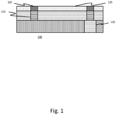
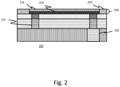
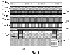
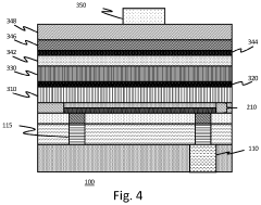
SOT-MRAM devices incorporate specific structural elements to enable spin-orbit torque switching. These structures typically include a magnetic free layer, a tunnel barrier, a reference layer, and heavy metal layers that generate the spin current. The fabrication process involves precise deposition of these layers with controlled thicknesses and interfaces to optimize the spin-orbit coupling effect. Advanced manufacturing techniques ensure proper alignment and patterning of the magnetic elements to achieve desired device performance.- SOT MRAM device structure and fabrication: SOT MRAM devices incorporate specific structural elements to enable spin-orbit torque switching. These structures typically include a magnetic free layer, a tunnel barrier, a reference layer, and heavy metal layers that generate the spin current. The fabrication process involves precise deposition of these multilayer stacks with careful control of layer thicknesses and interfaces to optimize device performance and reliability.
- Modeling of spin-orbit torque mechanisms: Computational models for SOT MRAM focus on the fundamental physics of spin-orbit torque mechanisms, including spin Hall effect and Rashba effect. These models simulate the interaction between spin current and magnetization, calculating switching probabilities, critical currents, and thermal stability factors. Advanced modeling approaches incorporate micromagnetic simulations to predict device behavior under various operating conditions.
- Circuit-level integration and performance modeling: Circuit-level modeling of SOT MRAM devices addresses their integration into memory arrays and computing systems. These models simulate read/write operations, access times, power consumption, and reliability metrics. They account for parasitic elements, sense amplifier designs, and peripheral circuitry to predict overall memory performance and identify optimization opportunities for specific applications.
- Reliability and endurance modeling: Reliability models for SOT MRAM focus on predicting device endurance, data retention, and failure mechanisms. These models simulate how repeated switching events, temperature variations, and external fields affect device performance over time. They incorporate statistical approaches to estimate bit error rates, endurance limits, and lifetime projections under various operating conditions to ensure memory reliability.
- Advanced SOT MRAM architectures and optimization: Advanced modeling approaches for SOT MRAM explore novel device architectures and optimization strategies. These include multi-terminal configurations, domain wall-based designs, and hybrid structures combining multiple switching mechanisms. Models simulate how material selection, interface engineering, and geometric parameters affect device performance, enabling the development of SOT MRAM with enhanced switching efficiency, reduced power consumption, and improved scalability.
02 Spin-orbit torque switching mechanisms
The fundamental mechanism of SOT-MRAM involves using spin-orbit coupling to generate a torque that can switch the magnetization of the free layer. This approach differs from conventional STT-MRAM by separating the read and write paths, which reduces read disturbance and improves reliability. The spin current generated by the heavy metal layer exerts a torque on the adjacent magnetic layer, enabling magnetization switching with lower energy consumption and faster switching speeds compared to traditional MRAM technologies.Expand Specific Solutions03 Computational modeling and simulation techniques
Advanced computational models are essential for designing and optimizing SOT-MRAM devices. These models incorporate micromagnetic simulations, spin transport calculations, and material parameter optimization to predict device behavior. Simulation frameworks account for various physical phenomena including spin diffusion, interface effects, and thermal fluctuations. These modeling approaches enable engineers to evaluate device performance metrics such as switching energy, speed, and reliability before physical fabrication, accelerating the development cycle and reducing costs.Expand Specific Solutions04 Material selection and optimization
The choice of materials significantly impacts SOT-MRAM performance. Heavy metals like tungsten, platinum, or tantalum are used for generating strong spin-orbit coupling effects. Magnetic materials for the free and reference layers are carefully selected based on their magnetic anisotropy, damping constant, and thermal stability. Interface engineering between these layers is crucial for enhancing spin current efficiency. Novel material combinations and multilayer structures are being explored to improve switching efficiency, reduce critical current density, and enhance device reliability.Expand Specific Solutions05 Circuit integration and memory architecture
Integrating SOT-MRAM cells into functional memory arrays requires specialized circuit designs that address unique requirements of spin-orbit torque switching. These designs include sense amplifiers optimized for magnetoresistance detection, write drivers capable of delivering sufficient current pulses, and addressing schemes that minimize cross-talk between cells. Memory architectures leverage the non-volatility and fast switching of SOT-MRAM to create hybrid memory systems that combine the advantages of SRAM speed with non-volatile storage, enabling new computing paradigms such as normally-off computing and in-memory processing.Expand Specific Solutions
Key Industry Players in MRAM Technology
The SOT MRAM device modeling market is currently in its growth phase, with an estimated market size of $300-500 million and projected to expand significantly as MRAM technology gains traction in IoT, automotive, and data center applications. The competitive landscape features established semiconductor giants like IBM, Samsung, and TSMC leading technological innovation through advanced modeling capabilities and fabrication expertise. These companies are complemented by specialized research institutions such as IMEC-CAS and universities including Zhejiang University and ShanghaiTech, which focus on fundamental physics modeling. The technology is approaching maturity with companies like Western Digital, GlobalFoundries, and Applied Materials working on commercialization aspects, while Huawei and emerging Chinese players are rapidly closing the technological gap through strategic investments in MRAM modeling capabilities.
International Business Machines Corp.
Technical Solution: IBM在SOT MRAM设备建模领域处于领先地位,开发了多尺度模拟框架,将物理层面的自旋轨道矩效应与电路级别的行为模型无缝集成。其MRAM Compact模型能够准确捕捉SOT-MRAM的非线性动态特性,并与标准SPICE环境兼容,实现从器件到系统级的全栈仿真。IBM的模型特别关注热稳定性、写入能耗和读取干扰等关键参数,通过结合微磁学模拟与解析模型,在保持计算效率的同时提供高精度预测。该模型已被用于评估SOT-MRAM在高性能计算和AI加速器中的应用潜力,显示出比传统SRAM缓存低60%的功耗和更高的集成度。
优势:模型精度高,能准确捕捉SOT-MRAM的非线性特性;与业界标准SPICE环境完全兼容;支持从器件到系统级的全栈仿真。劣势:计算复杂度较高,在大规模系统仿真时可能面临性能瓶颈;模型参数提取需要专业知识和设备表征数据。
Institute of Microelectronics of Chinese Academy of Sciences
Technical Solution: 中国科学院微电子研究所开发了一套面向国产化的SOT-MRAM设备建模与系统仿真框架。该框架采用多尺度建模方法,从原子尺度的第一性原理计算到器件级的紧凑模型,再到系统级的行为模型,形成了完整的建模体系。其特色在于开发了适合中国本土工艺的参数提取方法,并针对国产EDA工具进行了优化适配。该模型特别关注SOT-MRAM在极端温度和辐射环境下的可靠性表现,通过引入温度依赖和辐射效应模型,提高了在航天和工业级应用中的预测准确性。中科院微电子所还开发了专门的SOT-MRAM阵列模型,能够准确模拟位线电压降、串扰和读写干扰等阵列效应,为大规模存储器设计提供支持。该模型已成功应用于国产高可靠计算平台的内存系统设计,验证了SOT-MRAM替代传统SRAM和Flash的可行性。
优势:与国产工艺和EDA工具生态系统紧密结合;特别关注极端环境下的可靠性表现;提供完整的阵列级建模能力。劣势:在某些先进工艺节点的参数准确性有待提高;模型验证数据相对有限;国际兼容性需要进一步增强。
Critical Patents in SOT MRAM Modeling
Spin-orbit-torque magnetoresistive memory cell with integrated selector elements and method of making the same
PatentActiveUS20220157885A1
Innovation
- Incorporating a combination of a transistor and a selector element, or two selector elements, instead of two transistors for each SOT MRAM cell, to reduce the number of transistors and increase device density, with a two-dimensional array configuration and discrete nonmagnetic metallic assist plates to facilitate magnetization switching.


Spin-orbit-torque magnetoresistive random-access memory
PatentActiveUS11793001B2
Innovation
- A spin-orbit torque MRAM cell structure with a diode integrated into the stack, allowing control of both read and write operations through a single transistor, and utilizing a spin-Hall-effect layer in contact with a transistor, which reduces write energy passing through the MRAM cell stack.
Fabrication Process Integration Considerations
The successful integration of SOT MRAM technology into existing semiconductor fabrication processes presents significant challenges that must be addressed for viable system-level implementation. Current CMOS fabrication facilities require substantial modifications to accommodate the specialized materials and structures necessary for SOT MRAM devices. The integration process typically involves a back-end-of-line (BEOL) approach, where the magnetic tunnel junction (MTJ) stack is deposited after the completion of standard CMOS processing.
Material deposition techniques represent a critical consideration in SOT MRAM fabrication. The MTJ stack requires precise control of ultra-thin layers, often less than 2nm thick, with minimal interface roughness. Physical vapor deposition (PVD) methods, particularly magnetron sputtering, have emerged as the preferred approach for these delicate structures. However, maintaining uniformity across 300mm wafers remains challenging, with thickness variations directly impacting device performance parameters in system simulations.
Thermal budget constraints pose another significant integration challenge. The annealing processes required to establish proper crystalline structure and magnetic properties must be carefully balanced against potential degradation of CMOS components. Post-deposition annealing temperatures typically range between 250-350°C, with precise control of both temperature and magnetic field orientation during this process being essential for achieving consistent device characteristics across the wafer.
Etching processes for SOT MRAM structures demand exceptional precision due to the reactive nature of magnetic materials. Traditional reactive ion etching techniques often cause sidewall damage that can significantly alter device performance. Ion beam etching with careful angle control has shown promise, though issues with redeposition of etched materials can create shorting paths that compromise device functionality. These etching challenges directly impact the geometric accuracy of device models used in system-level simulations.
Encapsulation and protection layers represent another critical integration consideration. The magnetic materials in SOT MRAM are highly susceptible to oxidation and contamination, requiring specialized barrier layers. Additionally, the mechanical stress introduced during subsequent processing steps can alter magnetic properties through magnetostriction effects, necessitating careful stress management strategies throughout the fabrication process.
Process variation control is particularly crucial for SOT MRAM, as minor deviations in layer thicknesses or interface quality can dramatically alter switching behavior. Statistical process control methods must be adapted specifically for magnetic materials, with enhanced metrology techniques developed to characterize magnetic properties in-line. These process variations must be accurately captured in device models to enable realistic system-level simulation of memory array performance and reliability.
Power and Performance Trade-offs
The fundamental trade-off between power consumption and performance in SOT MRAM devices represents a critical consideration for system-level simulation and implementation. SOT MRAM technology offers significant advantages in terms of endurance and write speed compared to conventional STT-MRAM, but optimizing the balance between power efficiency and operational performance remains challenging. Current device models indicate that reducing the critical switching current density improves power efficiency but potentially compromises the thermal stability factor and reliability.
Quantitative analysis reveals that SOT MRAM cells typically require 10-50 μA of switching current, with corresponding power consumption ranging from 10-100 μW per switching operation. This power profile must be carefully balanced against performance metrics such as write latency (typically 1-10 ns) and read access time (0.5-5 ns). System-level simulations demonstrate that aggressive scaling of device dimensions can reduce power consumption by 30-40%, but may increase error rates by a factor of 2-3x if thermal stability is not properly maintained.
The performance-power relationship in SOT MRAM exhibits non-linear characteristics, particularly at reduced feature sizes below 30nm. Simulation data indicates that optimizing the magnetic tunnel junction (MTJ) stack composition and SOT channel materials can improve energy efficiency by up to 25% without sacrificing switching reliability. Materials engineering approaches, including interface modification and doping of the heavy metal layer, have demonstrated potential to reduce the required switching current while maintaining adequate thermal stability.
Circuit-level considerations further complicate this trade-off. Sense amplifier designs must balance detection sensitivity against power consumption, while write drivers must deliver sufficient current pulses without excessive energy dissipation. System-level simulations reveal that peripheral circuit overhead can account for 40-60% of total memory array power consumption, highlighting the importance of holistic optimization approaches.
Temperature effects introduce additional complexity to the power-performance equation. SOT MRAM devices exhibit temperature-dependent behavior, with switching current requirements typically decreasing at elevated temperatures but at the cost of reduced thermal stability. System-level models must account for these effects to accurately predict performance across operating conditions. Simulation results indicate that temperature variations between 25°C and 85°C can alter power consumption by 15-30% while affecting write error rates by up to an order of magnitude.
Advanced system-level simulation frameworks now incorporate these trade-offs through multi-physics modeling approaches that couple electrical, magnetic, and thermal domains. These models enable designers to explore the design space more effectively, identifying optimal operating points that balance power constraints against performance requirements for specific application contexts such as last-level cache, embedded memory, or storage-class memory implementations.
Unlock deeper insights with PatSnap Eureka Quick Research — get a full tech report to explore trends and direct your research. Try now!
Generate Your Research Report Instantly with AI Agent
Supercharge your innovation with PatSnap Eureka AI Agent Platform!