

SOT MRAM For Harsh Environment Electronics Radiation Tolerance
AUG 28, 20259 MIN READ
Generate Your Research Report Instantly with AI Agent
PatSnap Eureka helps you evaluate technical feasibility & market potential.
SOT MRAM Evolution and Radiation Hardening Goals
Spin-Orbit Torque Magnetoresistive Random Access Memory (SOT MRAM) represents a significant advancement in non-volatile memory technology, evolving from earlier generations of magnetic memory technologies. The development trajectory began with Toggle MRAM, progressed through Spin-Transfer Torque (STT) MRAM, and has now reached SOT MRAM, which offers superior performance characteristics including faster switching speeds, lower power consumption, and enhanced endurance.
The evolution of SOT MRAM technology has been driven by the fundamental need for radiation-hardened electronics in harsh environment applications. Traditional semiconductor memories, such as SRAM, DRAM, and Flash, exhibit significant vulnerabilities when exposed to radiation environments, including single event upsets (SEUs), total ionizing dose (TID) effects, and displacement damage. These vulnerabilities have created a persistent technological gap in critical sectors including aerospace, nuclear facilities, and military applications.
SOT MRAM's inherent radiation tolerance stems from its unique writing mechanism that utilizes spin-orbit coupling to manipulate magnetic states without requiring direct current flow through the magnetic tunnel junction (MTJ). This separation of read and write paths represents a fundamental architectural advantage over previous MRAM technologies, significantly reducing susceptibility to radiation-induced errors.
The primary radiation hardening goals for SOT MRAM development include achieving TID tolerance exceeding 1 Mrad(Si), SEU linear energy transfer (LET) thresholds above 40 MeV-cm²/mg, and operational stability across temperature extremes from -55°C to 125°C. Additionally, there are targets for data retention periods exceeding 10 years in radiation environments and write endurance capabilities surpassing 10^12 cycles under radiation exposure.
Recent technological breakthroughs have demonstrated promising results, with prototype SOT MRAM devices showing minimal performance degradation after exposure to gamma radiation doses up to 300 krad(Si). However, significant challenges remain in optimizing the material stack to further enhance radiation hardness while maintaining competitive performance metrics compared to commercial non-radiation-hardened memories.
The roadmap for SOT MRAM evolution focuses on several key technological improvements: developing novel heavy metal materials with enhanced spin-orbit coupling efficiency, engineering specialized tunnel barrier materials with improved radiation resistance, and implementing advanced error correction techniques specifically designed for radiation-induced failure modes in magnetic memories.
As the technology continues to mature, the ultimate goal is to establish SOT MRAM as the standard memory solution for harsh environment electronics, offering an optimal balance of radiation hardness, non-volatility, speed, and energy efficiency that cannot be matched by alternative memory technologies in these specialized application domains.
Market Analysis for Radiation-Tolerant Memory Solutions
The radiation-tolerant memory market is experiencing significant growth driven by expanding applications in aerospace, defense, nuclear energy, and high-reliability industrial sectors. Current market valuations place this specialized segment at approximately $2.1 billion globally, with projections indicating a compound annual growth rate of 7.8% through 2028. This growth trajectory is primarily fueled by increasing satellite deployments, space exploration missions, and defense modernization programs requiring radiation-hardened electronics.
SOT MRAM (Spin-Orbit Torque Magnetoresistive Random Access Memory) is positioned to capture a growing share of this market due to its inherent radiation tolerance advantages over conventional memory technologies. Traditional radiation-hardened memory solutions like rad-hard SRAM and MRAM command premium pricing, typically 10-20 times higher than commercial-grade equivalents, reflecting the specialized manufacturing processes and rigorous qualification requirements.
Geographically, North America dominates the radiation-tolerant memory market with approximately 45% market share, driven by NASA, Department of Defense, and major aerospace contractors. Europe follows at 28%, with significant contributions from ESA programs and defense initiatives. The Asia-Pacific region, particularly Japan and China, is the fastest-growing market segment with 15-18% annual growth as these nations expand their space programs and defense capabilities.
Customer segmentation reveals that government/military applications currently represent 62% of demand, followed by commercial space at 24%, and nuclear/industrial applications at 14%. The commercial space segment is expected to grow most rapidly due to the proliferation of small satellite constellations and commercial space ventures requiring radiation-tolerant components at more accessible price points.
Key market drivers include the miniaturization of satellites, increasing data processing requirements in space, longer mission durations, and the trend toward commercial off-the-shelf (COTS) components with radiation tolerance. SOT MRAM specifically addresses market demands for non-volatile memory solutions that combine radiation hardness with low power consumption, high endurance, and fast read/write speeds.
Market barriers include high development and qualification costs, long certification cycles (typically 2-3 years for space applications), and limited production volumes that challenge economies of scale. Additionally, the market faces supply chain vulnerabilities due to the specialized nature of radiation-hardened component manufacturing and geopolitical factors affecting access to critical materials and technologies.
SOT MRAM Technology Status and Radiation Challenges
Spin-Orbit Torque Magnetic Random Access Memory (SOT MRAM) represents a significant advancement in non-volatile memory technology, offering potential advantages in radiation-harsh environments compared to conventional memory solutions. The current global development status of SOT MRAM shows promising progress, with research institutions and semiconductor companies achieving significant breakthroughs in recent years.
The fundamental technology of SOT MRAM has evolved from earlier MRAM variants, utilizing spin-orbit coupling effects to manipulate magnetic states without requiring direct current flow through the magnetic tunnel junction (MTJ). This separation of read and write paths represents a critical advantage for radiation tolerance, as it reduces vulnerability to single-event effects that can plague conventional memory cells.
Despite these advances, SOT MRAM faces several technical challenges in harsh radiation environments. Total Ionizing Dose (TID) effects can degrade peripheral CMOS circuitry, while Single Event Effects (SEEs) may still impact control logic. The magnetic tunnel junction itself, while inherently more radiation-resistant than charge-based storage mechanisms, remains susceptible to displacement damage from heavy ions and neutrons at extreme radiation levels.
Current radiation testing data indicates that SOT MRAM exhibits superior performance compared to conventional MRAM and other non-volatile memories when exposed to radiation. Tests conducted at various radiation facilities have demonstrated functionality up to several hundred krad(Si) for TID and relatively high Linear Energy Transfer (LET) thresholds for Single Event Upsets (SEUs), though comprehensive standardized testing across different manufacturers remains limited.
Geographically, SOT MRAM development is concentrated in several key regions. The United States maintains leadership through companies like Everspin Technologies and research at institutions such as MIT and Stanford. In Asia, South Korean and Japanese firms including Samsung and Toshiba have made significant investments, while European efforts are centered around IMEC in Belgium and CEA-Leti in France.
The radiation hardening approaches for SOT MRAM currently follow two main strategies: intrinsic hardening through materials engineering and extrinsic hardening through circuit-level techniques. Materials research focuses on developing radiation-resistant tunnel barriers and magnetic layers, while circuit-level approaches implement error correction codes and redundancy schemes to mitigate radiation effects.
The technology readiness level (TRL) of radiation-hardened SOT MRAM currently stands at approximately 4-5, indicating component validation in laboratory environments with limited radiation testing. This positions the technology as promising but requiring further development before widespread deployment in mission-critical space, defense, or nuclear applications where extreme radiation tolerance is essential.
Current SOT MRAM Radiation Hardening Approaches
01 SOT-MRAM radiation hardening techniques
Spin-Orbit Torque Magnetic Random Access Memory (SOT-MRAM) can be designed with specific radiation hardening techniques to improve tolerance against radiation effects. These techniques include specialized material selection, shielding layers, and circuit design modifications that protect the magnetic tunnel junctions from radiation-induced errors. The radiation hardening approaches enable SOT-MRAM to maintain data integrity and operational stability in high-radiation environments such as space applications.- SOT-MRAM structure for enhanced radiation tolerance: Spin-Orbit Torque Magnetic Random Access Memory (SOT-MRAM) can be designed with specific structural modifications to enhance radiation tolerance. These designs include specialized layer configurations, material selections, and geometric arrangements that minimize the impact of radiation-induced effects. The radiation-hardened structures maintain data integrity and device performance when exposed to harsh radiation environments, making them suitable for aerospace and military applications.
- Radiation shielding techniques for SOT-MRAM: Various shielding techniques can be implemented to protect SOT-MRAM devices from radiation damage. These include incorporating radiation-absorbing materials, implementing buffer layers, and designing specialized encapsulation methods. The shielding approaches effectively reduce the flux of ionizing radiation reaching sensitive magnetic components, thereby preserving the magnetic state information and extending device lifetime in radiation-intensive environments.
- Error correction mechanisms for radiation-induced faults: SOT-MRAM devices can incorporate specialized error detection and correction mechanisms to address radiation-induced faults. These systems include redundant storage elements, parity checking, and advanced error correction codes specifically designed to handle single-event upsets and other radiation effects. By implementing these mechanisms, the reliability of SOT-MRAM in radiation environments is significantly improved without substantial performance penalties.
- Material engineering for radiation-hardened SOT-MRAM: Advanced materials can be engineered specifically for radiation-hardened SOT-MRAM applications. These materials include specialized magnetic layers with higher coercivity, radiation-resistant tunnel barriers, and novel electrode materials that maintain their electrical and magnetic properties under radiation exposure. The careful selection and engineering of these materials significantly improve the radiation tolerance of SOT-MRAM devices while maintaining their performance advantages.
- Testing and qualification methods for radiation-tolerant SOT-MRAM: Specialized testing and qualification methodologies have been developed to evaluate the radiation tolerance of SOT-MRAM devices. These methods include accelerated radiation testing protocols, real-time monitoring techniques, and comprehensive qualification standards specifically designed for memory technologies in radiation environments. The testing approaches enable accurate assessment of SOT-MRAM performance under various radiation conditions, facilitating their certification for space, nuclear, and other high-radiation applications.
02 Comparative radiation tolerance of SOT-MRAM versus other memory technologies
SOT-MRAM demonstrates superior radiation tolerance compared to conventional memory technologies like SRAM, DRAM, and Flash memory. The inherent non-volatile nature and magnetic storage mechanism of SOT-MRAM make it less susceptible to radiation-induced soft errors and single event upsets. Studies show that SOT-MRAM maintains functionality at radiation levels that would cause failure in other memory types, making it particularly valuable for aerospace, military, and nuclear applications where radiation exposure is significant.Expand Specific Solutions03 Material innovations for radiation-resistant SOT-MRAM
Advanced material compositions can significantly enhance the radiation tolerance of SOT-MRAM devices. Incorporating heavy metals with high spin-orbit coupling, radiation-resistant ferromagnetic materials, and specialized barrier layers improves the stability of magnetic states under radiation exposure. These material innovations focus on maintaining the spin polarization efficiency and magnetic anisotropy even when subjected to high-energy particles, thereby preserving data integrity in radiation-intensive environments.Expand Specific Solutions04 SOT-MRAM architecture optimization for radiation environments
Architectural modifications to SOT-MRAM designs can enhance radiation tolerance through redundancy schemes, error correction mechanisms, and specialized sensing circuits. These optimizations include implementing multiple reference cells, differential sensing techniques, and radiation-aware layout designs that minimize the impact of radiation-induced transients. The architectural approaches focus on detecting and mitigating radiation effects at the system level, ensuring reliable operation in high-radiation environments without compromising performance or power efficiency.Expand Specific Solutions05 Testing and qualification methods for radiation-tolerant SOT-MRAM
Specialized testing protocols and qualification methodologies have been developed to evaluate and certify the radiation tolerance of SOT-MRAM devices. These methods include accelerated radiation testing, real-time monitoring during radiation exposure, and post-radiation performance analysis. The qualification procedures assess parameters such as data retention, write/read reliability, and error rates under various radiation conditions, providing standardized metrics for comparing radiation hardness across different SOT-MRAM implementations and ensuring suitability for mission-critical applications.Expand Specific Solutions
Key Industry Players in Radiation-Tolerant SOT MRAM
SOT MRAM for harsh environment electronics radiation tolerance is in an emerging growth phase, with the market expected to expand significantly due to increasing demand in aerospace, defense, and nuclear applications. The technology is approaching maturity, with key players demonstrating varied capabilities. Samsung Electronics and IBM lead commercial development with advanced radiation-hardened SOT MRAM solutions, while research institutions like Tohoku University and IMEC contribute fundamental breakthroughs. Taiwan Semiconductor and UMC provide manufacturing expertise, with Huawei and Western Digital exploring application-specific implementations. The competitive landscape shows a balance between established semiconductor giants and specialized research entities, with collaboration between industry and academia accelerating development toward radiation-tolerant memory solutions.
Samsung Electronics Co., Ltd.
Technical Solution: Samsung has developed radiation-tolerant SOT-MRAM technology as part of their comprehensive memory portfolio for harsh environment applications. Their approach leverages a specialized three-terminal SOT-MRAM cell design with enhanced radiation immunity through material engineering and architectural innovations. Samsung's radiation-hardened SOT-MRAM utilizes tungsten-based spin Hall channels with optimized thickness and doping profiles to minimize radiation-induced performance degradation. Their technology incorporates radiation-resistant capping layers and specialized barrier materials that prevent radiation-induced diffusion and maintain interface quality. Samsung has demonstrated SOT-MRAM arrays that maintain functionality after exposure to radiation doses of 100 krad(Si) and show resistance to single event upsets with LET thresholds above 37 MeV-cm²/mg. The technology is designed for integration with their radiation-hardened logic processes, enabling system-on-chip solutions for space, aviation, and nuclear applications requiring reliable non-volatile memory operation in radiation environments.
Strengths: Extensive manufacturing infrastructure and quality control systems; comprehensive memory ecosystem integration capabilities; strong roadmap for scaling to higher densities. Weaknesses: Primary focus on commercial applications with radiation hardening as secondary feature; less specialized radiation testing infrastructure compared to defense contractors; higher susceptibility to radiation-induced write errors compared to some competitors.
International Business Machines Corp.
Technical Solution: IBM has developed advanced SOT-MRAM technology specifically engineered for radiation-hardened environments. Their approach utilizes a perpendicular magnetic anisotropy (PMA) design with tungsten-based spin Hall channels that demonstrate enhanced radiation tolerance. IBM's SOT-MRAM architecture separates the read and write paths, significantly reducing vulnerability to radiation-induced errors. Their devices have demonstrated resilience against Total Ionizing Dose (TID) effects up to 1 Mrad(Si) and Single Event Effects (SEE) with Linear Energy Transfer (LET) thresholds exceeding 40 MeV-cm²/mg. IBM has implemented specialized shielding layers and redundant cell designs to further enhance radiation hardness while maintaining data retention capabilities in extreme temperature environments from -55°C to 125°C, making them suitable for aerospace and military applications.
Strengths: Superior radiation hardness with proven performance in high-radiation environments; excellent data retention at extreme temperatures; mature manufacturing process integration with CMOS technology. Weaknesses: Higher power consumption compared to conventional MRAM; relatively larger cell size due to additional radiation hardening features; higher production costs due to specialized materials and manufacturing processes.
Critical Patents in Radiation-Resistant SOT MRAM Design
Spin orbit torque MRAM and manufacture thereof
PatentWO2020106378A1
Innovation
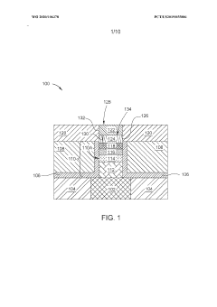
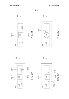
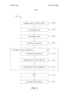
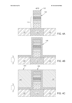
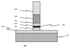
- The SOT-MRAM devices are fabricated with a bottom-pinned structure where the MTJ stack and SOT layer are formed in-situ without breaking vacuum, creating a high-quality interface and using an encapsulation layer to protect the free layer, with metal lines electrically coupling to the SOT layer on multiple sides to prevent current loss.
Spin-orbit torque magnetoresistive random access memory array
PatentPendingJP2024528302A
Innovation
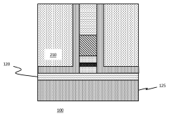
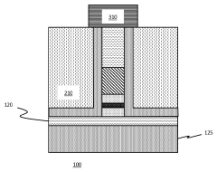
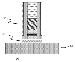
- Integration of SOT-MRAM cell stack with a diode in each unit cell, creating a more efficient array structure with improved cell selectivity.
- Column-based source line architecture that contacts source contacts of transistors in each column, combined with row-based SOT lines contacting drain contacts, enabling efficient cell addressing.
- Placement of unit cells above the SOT line with direct electrical connection, creating a more compact vertical integration that potentially improves density and performance.
Reliability Testing Methodologies for Radiation Environments
Testing the reliability of SOT MRAM devices in radiation environments requires specialized methodologies that accurately simulate and measure the effects of various radiation types. These methodologies must account for the unique failure mechanisms that occur in harsh environments such as space, nuclear facilities, and high-altitude aviation applications.
Total Ionizing Dose (TID) testing represents a fundamental approach, where devices are exposed to cumulative radiation doses using gamma ray or X-ray sources. For SOT MRAM evaluation, TID tests typically range from 30 krad to 1 Mrad, with electrical parameters measured at predetermined dose intervals to track performance degradation. This methodology helps identify threshold radiation levels where device functionality becomes compromised.
Single Event Effects (SEE) testing constitutes another critical methodology, focusing on transient radiation events. Heavy ion testing employs accelerator facilities to bombard devices with ions of varying Linear Energy Transfer (LET) values, typically ranging from 1 to 100 MeV-cm²/mg. Proton testing complements this approach, using proton beams with energies between 1-200 MeV to simulate cosmic radiation environments.
Neutron radiation testing has particular relevance for SOT MRAM applications in nuclear environments. This methodology employs research reactors or neutron generators to produce thermal and fast neutrons, with fluence levels typically ranging from 10¹⁰ to 10¹⁵ n/cm². The testing evaluates both immediate effects and long-term material degradation from neutron exposure.
In-situ testing methodologies provide real-time performance monitoring during radiation exposure, offering insights into transient effects that might be missed in pre/post-irradiation testing. This approach requires specialized test fixtures capable of operating in radiation environments while maintaining signal integrity for accurate measurements.
Accelerated testing protocols compress time scales by increasing radiation intensity, allowing lifetime predictions based on established acceleration factors. However, these methodologies must account for potential non-linear effects that may emerge at higher dose rates compared to actual operating conditions.
Statistical reliability methodologies are equally important, requiring sufficient sample sizes to establish confidence intervals for radiation tolerance specifications. Typically, 20-30 devices from multiple fabrication lots undergo testing to account for manufacturing variations that might affect radiation response.
Space and Nuclear Applications Integration Roadmap
The integration of SOT MRAM technology into space and nuclear applications follows a strategic roadmap that addresses the unique challenges of these extreme environments. Initially, qualification testing protocols must be established to evaluate SOT MRAM's performance under radiation exposure levels typical in Low Earth Orbit (LEO), Geosynchronous Earth Orbit (GEO), and nuclear facilities. These protocols will focus on Total Ionizing Dose (TID) tolerance, Single Event Effects (SEE) resilience, and displacement damage resistance.
By 2025-2027, the roadmap envisions the first deployment of SOT MRAM in non-critical satellite subsystems, serving as technology demonstrators while gathering real-world performance data. This phase will include integration with radiation-hardened peripheral circuits specifically designed to complement SOT MRAM's inherent radiation tolerance characteristics.
The mid-term phase (2028-2030) targets the expansion to mission-critical systems in spacecraft, including command and data handling subsystems, attitude determination and control systems, and onboard data storage. Simultaneously, initial implementations in nuclear power plant monitoring systems and radiation detection equipment will commence, leveraging lessons learned from space applications.
Long-term integration (2031-2035) focuses on developing fully radiation-hardened SOT MRAM-based computing platforms for deep space missions, including lunar bases and Mars expeditions, where radiation levels exceed those in Earth orbit. The nuclear sector will see integration into reactor control systems and safety-critical applications where traditional electronics face significant reliability challenges.
Throughout this roadmap, collaborative efforts between space agencies (NASA, ESA, JAXA), nuclear regulatory bodies, and semiconductor manufacturers will be essential to establish standardized testing methodologies and certification processes. These collaborations will accelerate the development of application-specific SOT MRAM variants optimized for particular radiation environments.
The roadmap also emphasizes the importance of developing specialized packaging solutions that enhance radiation shielding while maintaining the size, weight, and power advantages of SOT MRAM technology. Advanced error correction techniques and redundancy architectures specific to SOT MRAM implementation will be developed to further improve reliability in mission-critical applications.
By following this integration roadmap, SOT MRAM technology can transition from laboratory demonstrations to becoming the standard memory solution for harsh environment electronics, offering unprecedented data retention and processing capabilities in environments where conventional memory technologies fail.
Unlock deeper insights with PatSnap Eureka Quick Research — get a full tech report to explore trends and direct your research. Try now!
Generate Your Research Report Instantly with AI Agent
Supercharge your innovation with PatSnap Eureka AI Agent Platform!