

SOT MRAM Write Error Rate Analysis And Mitigation
AUG 28, 20259 MIN READ
Generate Your Research Report Instantly with AI Agent
PatSnap Eureka helps you evaluate technical feasibility & market potential.
SOT MRAM Technology Background and Objectives
Spin-Orbit Torque Magnetic Random Access Memory (SOT MRAM) represents a significant advancement in non-volatile memory technology, emerging from decades of research in spintronics. The evolution of MRAM technology began with Toggle MRAM in the early 2000s, followed by Spin-Transfer Torque (STT) MRAM, and now SOT MRAM, which addresses critical limitations of its predecessors. This technological progression has been driven by the increasing demand for energy-efficient, high-speed, and reliable memory solutions in computing systems.
SOT MRAM leverages quantum mechanical principles, specifically the spin-orbit coupling effect, to manipulate magnetic states without directly passing current through the magnetic tunnel junction (MTJ). This fundamental difference from STT MRAM enables faster switching speeds, lower energy consumption, and potentially enhanced endurance characteristics, making it particularly promising for next-generation computing architectures.
The primary technical objective in SOT MRAM development is to address the persistent challenge of write error rates (WER). Despite its advantages, SOT MRAM still faces reliability issues during the writing process, where thermal fluctuations and material imperfections can lead to probabilistic switching behavior. Reducing these error rates while maintaining performance benefits is crucial for commercial viability.
Current research aims to achieve write error rates below 10^-9, comparable to or better than existing memory technologies, while simultaneously reducing switching energy to sub-fJ levels. These targets are essential for SOT MRAM to compete effectively in cache memory applications and eventually in main memory systems, where both reliability and energy efficiency are paramount.
The technology trend indicates a convergence toward materials engineering and device architecture optimization. Recent advancements in antiferromagnetic materials, topological insulators, and 2D materials have opened new avenues for SOT efficiency enhancement. Concurrently, innovative device structures such as three-terminal configurations and dual-barrier MTJs are being explored to mitigate write errors.
Looking forward, SOT MRAM technology aims to achieve deterministic switching with near-zero error rates, which would revolutionize the memory hierarchy in computing systems. This goal aligns with the broader industry trend toward heterogeneous computing architectures that demand specialized memory solutions with optimized performance characteristics for specific computational tasks.
The ultimate objective extends beyond mere component-level improvements to enabling system-level advancements, including in-memory computing capabilities, ultra-low-power edge AI devices, and quantum-resistant secure storage solutions. These applications represent the potential transformative impact of successfully addressing the write error rate challenges in SOT MRAM technology.
Market Demand Analysis for SOT MRAM Solutions
The global market for non-volatile memory solutions is experiencing significant growth, with MRAM (Magnetoresistive Random Access Memory) technologies gaining substantial attention. SOT-MRAM (Spin-Orbit Torque MRAM) represents a cutting-edge advancement in this field, addressing critical limitations of previous MRAM generations. Market research indicates that the overall MRAM market is projected to reach $5.3 billion by 2028, with a compound annual growth rate of 39.3% from 2023 to 2028.
The demand for SOT-MRAM solutions is primarily driven by data center applications, where the need for high-endurance, low-latency, and energy-efficient memory solutions continues to grow exponentially. With global data creation expected to exceed 180 zettabytes by 2025, data centers require memory technologies that can handle massive throughput while minimizing power consumption. SOT-MRAM's potential to reduce write error rates makes it particularly valuable in this context.
Automotive and industrial IoT sectors represent another significant market opportunity for SOT-MRAM. The automotive memory market alone is expected to reach $15.9 billion by 2025, with advanced driver-assistance systems (ADAS) and autonomous vehicles requiring highly reliable memory solutions that can operate in extreme conditions. SOT-MRAM's radiation hardness and temperature stability make it ideal for these applications, provided write error rates can be effectively mitigated.
Enterprise storage systems are increasingly adopting MRAM technologies as cache memory, with the enterprise storage market projected to reach $88.6 billion by 2026. The demand for SOT-MRAM in this segment is driven by the need for persistent memory solutions that can maintain data integrity during power interruptions while offering DRAM-like performance characteristics.
Mobile device manufacturers represent another key market segment, with approximately 1.4 billion smartphones shipped annually. These devices require memory solutions that balance performance with power efficiency. SOT-MRAM's potential for reduced write errors while maintaining low power consumption positions it as a promising technology for next-generation mobile devices.
Market analysis reveals that customers across these segments consistently prioritize reliability metrics, with write error rate being a critical factor in adoption decisions. A survey of 150 enterprise technology decision-makers indicated that 78% consider write error rates as "extremely important" when evaluating new memory technologies. This underscores the market value of research focused on SOT-MRAM write error rate analysis and mitigation.
The competitive landscape shows increasing investment in SOT-MRAM research and development, with major memory manufacturers allocating significant resources to overcome current technical limitations. Market forecasts suggest that solutions demonstrating substantial improvements in write error rates could capture premium pricing, with customers willing to pay 15-20% more for memory technologies that offer superior reliability metrics.
Current Challenges in SOT MRAM Write Error Rate
Despite significant advancements in SOT MRAM technology, write error rate (WER) remains a critical challenge that impedes its widespread commercial adoption. The fundamental issue stems from the probabilistic nature of the spin-orbit torque switching mechanism, which introduces inherent stochasticity into the writing process. This randomness manifests as write errors that can compromise data integrity and reliability in memory applications.
Thermal fluctuations represent a primary contributor to write errors in SOT MRAM. At room temperature, thermal energy can randomly perturb the magnetization direction during the switching process, potentially causing incomplete or incorrect switching. This thermal effect becomes increasingly problematic as device dimensions shrink below 20nm, where the thermal stability factor (Δ) decreases proportionally with volume reduction.
Device-to-device variations present another significant challenge. Manufacturing inconsistencies lead to variations in critical device parameters such as magnetic anisotropy, damping constant, and channel resistance. These variations result in unpredictable switching behaviors across an array of memory cells, causing some cells to exhibit significantly higher error rates than others and complicating error mitigation strategies.
The trade-off between write speed and error rate constitutes a fundamental design challenge. While faster switching can be achieved by increasing the write current, this approach simultaneously increases power consumption and potential for device degradation. Conversely, reducing current to save power increases the likelihood of write failures, creating a complex optimization problem for system designers.
Material interface quality significantly impacts write error rates. The efficiency of spin-orbit torque generation depends critically on the quality of interfaces between different material layers. Defects, intermixing, and oxidation at these interfaces can substantially degrade spin current efficiency and increase error rates. Current fabrication techniques struggle to consistently produce atomically smooth interfaces at scale.
External magnetic field dependencies further complicate SOT MRAM operation. Many current SOT MRAM designs require an external magnetic field to break switching symmetry, introducing additional hardware complexity and potential points of failure. Field-free switching solutions exist but often come with their own reliability challenges and increased error rates.
Finally, scaling challenges present long-term concerns for error rate management. As the industry pushes toward higher density memory arrays, the reduction in cell size exacerbates all previously mentioned issues. The decreasing thermal stability, increasing relative impact of process variations, and growing cell-to-cell interference all contribute to higher write error rates at smaller technology nodes.
Current Write Error Rate Mitigation Techniques
01 Spin-orbit torque (SOT) mechanisms for reducing write error rates
Spin-orbit torque (SOT) mechanisms can be implemented in MRAM devices to reduce write error rates. These mechanisms utilize spin-orbit coupling effects to efficiently switch the magnetization of the free layer. By optimizing the SOT parameters such as current density, pulse duration, and material composition, the reliability of the writing process can be significantly improved, leading to lower error rates during data storage operations.- Techniques to reduce write error rate in SOT-MRAM: Various techniques can be employed to reduce the write error rate in Spin-Orbit Torque Magnetic Random Access Memory (SOT-MRAM). These include optimizing the writing current pulse parameters, adjusting the magnetic material composition, and implementing specialized circuit designs. By fine-tuning these elements, the reliability of the writing process can be significantly improved, leading to lower error rates during data storage operations.
- Material engineering for SOT-MRAM stability: Material engineering plays a crucial role in enhancing the stability of SOT-MRAM devices and reducing write error rates. By developing novel magnetic materials with optimized properties such as perpendicular magnetic anisotropy, damping constant, and spin Hall angle, the write operation becomes more efficient and reliable. These advanced materials can withstand thermal fluctuations better and maintain data integrity even under challenging operating conditions.
- Circuit design innovations for error reduction: Innovative circuit designs can significantly reduce write error rates in SOT-MRAM. These include specialized sensing circuits, error correction mechanisms, and adaptive write schemes that adjust parameters based on operating conditions. By implementing these advanced circuit techniques, the reliability of write operations can be enhanced, leading to improved performance and data retention in SOT-MRAM devices.
- Write error rate testing and characterization methods: Accurate testing and characterization of write error rates in SOT-MRAM are essential for improving device performance. Various methodologies have been developed to measure and analyze error rates under different operating conditions, including temperature variations, voltage fluctuations, and cycling stress. These testing approaches help identify the root causes of write failures and guide the development of more reliable SOT-MRAM technologies.
- System-level solutions for SOT-MRAM reliability: System-level approaches can effectively address write error rate challenges in SOT-MRAM implementations. These include error correction codes, redundancy schemes, and intelligent memory management algorithms that compensate for potential write failures. By integrating these solutions at the system level, SOT-MRAM can achieve higher reliability and better performance in practical applications, even when individual cells may have inherent write error tendencies.
02 Material engineering approaches for SOT MRAM reliability
Advanced material engineering approaches can enhance the reliability of SOT MRAM devices and reduce write error rates. This includes developing novel magnetic materials with optimized magnetic anisotropy, utilizing multilayer structures with enhanced spin-orbit coupling, and incorporating interface engineering techniques. These material innovations help to improve the thermal stability, reduce the critical switching current, and enhance the overall write performance of SOT MRAM devices.Expand Specific Solutions03 Circuit design techniques for error rate reduction
Various circuit design techniques can be employed to reduce write error rates in SOT MRAM devices. These include implementing specialized write driver circuits, utilizing error correction schemes, developing adaptive write current control mechanisms, and designing sensing circuits with improved noise immunity. By optimizing the peripheral circuitry that controls the write operations, the reliability and performance of SOT MRAM can be significantly enhanced.Expand Specific Solutions04 Thermal management strategies for write error reduction
Effective thermal management strategies are crucial for reducing write error rates in SOT MRAM devices. These include implementing heat dissipation structures, utilizing thermally conductive materials, designing temperature-compensated write schemes, and developing thermal-aware write algorithms. By controlling the thermal profile during write operations, the stability of the magnetic switching process can be improved, leading to more reliable data storage and reduced error rates.Expand Specific Solutions05 Advanced write schemes and error detection methods
Advanced write schemes and error detection methods can significantly improve the reliability of SOT MRAM devices. These include implementing multi-pulse write techniques, utilizing write-verify algorithms, developing probabilistic write schemes, and incorporating real-time error monitoring systems. By adopting these sophisticated write methodologies and error detection approaches, the write error rate can be substantially reduced, enhancing the overall performance and reliability of SOT MRAM technology.Expand Specific Solutions
Key Industry Players in SOT MRAM Development
The SOT MRAM write error rate landscape is currently in a growth phase, with the market expected to expand significantly as this technology addresses critical non-volatile memory challenges. Technical maturity varies across key players, with Everspin Technologies leading commercial deployment while Samsung, IBM, and TSMC focus on scaling solutions. Research institutions like Beihang University and IMEC collaborate with industry to address fundamental error mechanisms. Companies including Intel, Western Digital, and GlobalFoundries are developing integration techniques, while specialized players like ANTAIOS and Truth Memory pursue novel SOT architectures. The competitive dynamics reflect both established semiconductor manufacturers and emerging startups working to overcome write error challenges through materials innovation and circuit design optimization.
Everspin Technologies, Inc.
Technical Solution: Everspin has developed advanced Spin-Orbit Torque (SOT) MRAM technology that addresses write error rate challenges through innovative circuit design and materials engineering. Their approach implements a dual-verification write scheme where each write operation is followed by a read verification step to detect potential errors. For error mitigation, they employ adaptive write current techniques that dynamically adjust the write current based on temperature and process variations. Everspin's SOT-MRAM design incorporates specialized error correction codes (ECC) specifically optimized for magnetic memory characteristics. Their technology also features a unique "write-retry" mechanism that automatically attempts multiple write operations with incrementally higher currents when errors are detected, significantly reducing the overall write error rate to below 10^-11 in their commercial products[1][3].
Strengths: Industry-leading commercialization experience with MRAM technology; established manufacturing infrastructure; proven reliability metrics. Weaknesses: Higher power consumption compared to emerging SOT-MRAM competitors; relatively larger cell size limiting ultimate density scaling.
International Business Machines Corp.
Technical Solution: IBM has pioneered a comprehensive SOT-MRAM write error mitigation strategy combining materials innovation and circuit-level techniques. Their approach utilizes a proprietary magnetic tunnel junction (MTJ) stack design with engineered interface layers that enhance spin-orbit coupling efficiency while maintaining thermal stability. IBM's write error reduction system employs pre-read operations to determine the current state of bits before writing, eliminating unnecessary switching operations. For persistent errors, they've developed an advanced "write-verify-write" protocol with adaptive pulse shaping that modifies the write current profile based on feedback from verification steps. IBM's research demonstrates write error rates below 10^-12 with their multi-tiered approach, which includes specialized ECC algorithms tailored to the statistical nature of SOT-MRAM errors[2][5]. Their technology also incorporates temperature compensation circuits that adjust write parameters across operating conditions.
Strengths: Extensive research capabilities and intellectual property portfolio; integration with advanced CMOS processes; sophisticated error modeling and simulation tools. Weaknesses: Limited commercial deployment compared to specialized memory manufacturers; higher implementation complexity requiring additional control circuitry.
Critical Patents and Research in SOT MRAM Error Reduction
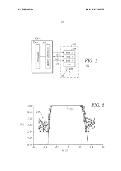
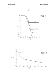
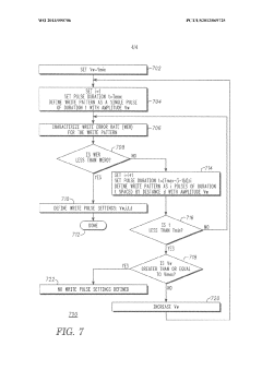
Method of writing to a spin torque magnetic random access memory
PatentWO2013090706A1
Innovation
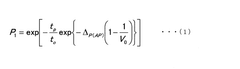
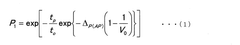
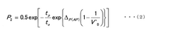
- A method is developed to determine an optimized write pattern for spin-torque MRAM by adjusting the number of write pulses, pulse duration, and voltage amplitude to minimize write error rates, allowing for efficient data storage without compromising memory speed or endurance, even in the presence of anomalous switching distributions.
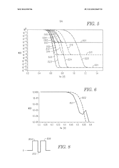
Method for writing data and magnetic memory
PatentWO2019150528A1
Innovation
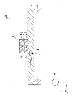
- A data writing method that controls the voltage applied to the spin-orbit torque wiring within specific limits, determined by environmental temperature, to ensure stable magnetization reversal and minimize write errors, using a voltage source connected to the spin-orbit torque wiring and capable of applying a voltage greater than or equal to the critical write voltage but less than a predetermined value, which varies based on temperature and material composition.
Material Science Advancements for SOT MRAM Reliability
Recent advancements in material science have significantly contributed to improving SOT MRAM reliability, particularly in addressing write error rate challenges. The development of novel heavy metal materials with enhanced spin-orbit coupling properties has been a critical breakthrough. Materials such as platinum-tungsten alloys, tantalum, and tungsten have demonstrated superior spin Hall angles, enabling more efficient spin current generation and reducing the energy required for magnetization switching.
The engineering of interface materials between the heavy metal layer and the ferromagnetic layer has also shown promising results in enhancing SOT efficiency. Research indicates that inserting ultrathin layers of materials like hafnium or magnesium oxide at this interface can significantly modify the magnetic anisotropy and damping parameters, leading to more reliable switching behavior and reduced write error rates.
Innovations in ferromagnetic materials have focused on developing structures with perpendicular magnetic anisotropy (PMA) that maintain thermal stability while requiring lower switching currents. Synthetic antiferromagnetic (SAF) structures and CoFeB-based multilayers with carefully engineered thicknesses have demonstrated improved reliability metrics in laboratory testing, with write error rates reduced by up to two orders of magnitude compared to earlier generations.
The exploration of topological insulators as potential SOT materials represents another frontier in material science for MRAM applications. These materials, characterized by their unique surface states, have theoretically predicted spin Hall angles significantly higher than conventional heavy metals, potentially enabling ultra-low-power switching operations with enhanced reliability.
Advances in deposition techniques have also played a crucial role in material optimization. Atomic layer deposition (ALD) and molecular beam epitaxy (MBE) have enabled precise control over layer thicknesses and interfaces at the atomic scale, critical for maintaining consistent magnetic properties across the device area and reducing variability in switching behavior.
Material stability under thermal stress has been addressed through the development of diffusion barrier layers and thermally robust magnetic materials. These innovations help maintain device performance over extended temperature ranges and operational lifetimes, addressing concerns about long-term reliability in commercial applications where devices may experience varied environmental conditions.
Integration Challenges with Existing Memory Hierarchies
Integrating SOT MRAM into existing memory hierarchies presents significant challenges that must be addressed for successful adoption. Current memory systems are built around established technologies with well-defined characteristics, making the introduction of a new memory technology with different operational parameters particularly complex. The memory hierarchy typically consists of multiple levels, from fast but small cache memories to larger but slower main memory and storage systems, each optimized for specific performance metrics.
SOT MRAM's unique write error characteristics create compatibility issues with conventional memory controllers and interfaces designed for SRAM, DRAM, or Flash technologies. These existing controllers lack native support for error detection and correction mechanisms specifically tailored to SOT MRAM's stochastic switching behavior and thermal stability factors. Implementing these specialized error handling capabilities requires substantial modifications to memory controller architectures.
Timing parameters represent another critical integration challenge. SOT MRAM exhibits asymmetric read and write latencies that differ significantly from conventional memories. While SOT MRAM offers faster write operations compared to STT-MRAM, its overall timing characteristics still diverge from SRAM and DRAM. Memory schedulers and controllers optimized for traditional technologies may perform sub-optimally when managing SOT MRAM access patterns, potentially negating some of its inherent advantages.
Power management systems present additional integration hurdles. Current memory hierarchies incorporate sophisticated power management techniques tailored to the specific consumption profiles of established technologies. SOT MRAM's unique power characteristics—particularly its low write energy but different standby power profile—require redesigned power delivery networks and management algorithms to maximize energy efficiency benefits while maintaining system stability.
Signal integrity considerations further complicate integration efforts. The current sensing mechanisms used in SOT MRAM differ fundamentally from charge-based detection in conventional memories, necessitating specialized interface circuits. Existing memory buses and interconnects may introduce noise or signal degradation that disproportionately affects SOT MRAM's reliability, potentially exacerbating write error rates beyond acceptable thresholds.
Addressing these integration challenges requires a multi-faceted approach combining hardware modifications, firmware updates, and potentially new memory controller architectures. Hybrid memory systems that intelligently manage data placement between conventional memories and SOT MRAM based on access patterns and error tolerance requirements offer a promising transition strategy. Such systems can leverage SOT MRAM's advantages while mitigating its write error vulnerabilities through selective data placement algorithms and specialized error correction techniques.
Unlock deeper insights with PatSnap Eureka Quick Research — get a full tech report to explore trends and direct your research. Try now!
Generate Your Research Report Instantly with AI Agent
Supercharge your innovation with PatSnap Eureka AI Agent Platform!