SOT MRAM For Non Volatile Logic In Memory Architectures
AUG 28, 20259 MIN READ
Generate Your Research Report Instantly with AI Agent
Patsnap Eureka helps you evaluate technical feasibility & market potential.
SOT MRAM Technology Background and Objectives
Spin-Orbit Torque Magnetic Random Access Memory (SOT MRAM) has emerged as a promising technology in the evolution of non-volatile memory solutions. The development of SOT MRAM traces back to the early 2010s, building upon the foundation established by Spin-Transfer Torque MRAM (STT-MRAM). The key innovation in SOT MRAM lies in its separation of read and write paths, which addresses the reliability and endurance limitations inherent in earlier MRAM technologies.
The technological trajectory of SOT MRAM has been characterized by significant advancements in materials science, particularly in the development of heavy metal/ferromagnet interfaces that facilitate efficient spin-orbit coupling. This evolution has been driven by the increasing demand for memory solutions that combine the speed of SRAM, the density of DRAM, and the non-volatility of flash memory, while consuming minimal power.
The primary objective of SOT MRAM development is to create a universal memory solution that can serve as both working memory and storage, effectively bridging the traditional memory hierarchy gap. For Logic In Memory architectures specifically, SOT MRAM aims to enable computational elements that retain their state without power, thereby dramatically reducing energy consumption in computing systems while maintaining high performance.
Current technical goals include achieving write speeds below 1ns, reducing critical switching current density to enable compatibility with advanced CMOS nodes, and ensuring thermal stability for reliable data retention at reduced feature sizes. These objectives are crucial for SOT MRAM to compete effectively with established memory technologies in various application domains.
The integration of SOT MRAM into Logic In Memory architectures represents a paradigm shift in computing, potentially enabling new computational models that leverage the unique properties of magnetic materials. This approach aims to overcome the von Neumann bottleneck by reducing data movement between separate memory and processing units, which currently accounts for a significant portion of energy consumption in computing systems.
Research efforts are increasingly focused on demonstrating practical implementations of SOT MRAM-based logic functions, including magnetic logic gates, look-up tables for FPGAs, and neuromorphic computing elements. These developments align with the broader industry trend toward specialized computing architectures optimized for specific workloads, particularly in artificial intelligence and edge computing applications.
The convergence of SOT MRAM technology with advanced CMOS processes represents a critical milestone in this technological evolution, as it will determine the commercial viability and widespread adoption of these novel computing paradigms. The ultimate goal is to establish SOT MRAM as a foundational technology for the next generation of energy-efficient, high-performance computing systems.
Market Demand Analysis for Non-Volatile Logic
The global market for non-volatile logic solutions is experiencing significant growth, driven by the increasing demand for energy-efficient computing architectures. Current projections indicate that the non-volatile memory market will reach $100 billion by 2025, with SOT MRAM technology potentially capturing a substantial portion of this expanding sector. This growth is primarily fueled by the escalating need for computing systems that can maintain data integrity during power interruptions while minimizing energy consumption.
The demand for non-volatile logic is particularly pronounced in edge computing applications, where devices operate under constrained power conditions and require persistent data storage capabilities. Industry analysts report that edge computing deployments are growing at 30% annually, creating a substantial market opportunity for SOT MRAM-based non-volatile logic solutions that can address these specific requirements.
Data centers represent another significant market segment, with operators increasingly seeking technologies that can reduce the 7-10% of global electricity consumption currently attributed to these facilities. Non-volatile logic architectures offer promising pathways to reduce both operational power consumption and the energy required for data backup systems, potentially decreasing overall energy requirements by 25-40% compared to conventional architectures.
The automotive sector presents a rapidly expanding market for non-volatile logic, particularly with the rise of electric and autonomous vehicles. These applications demand computing systems that can instantly resume operation after power cycling while maintaining critical system states. Market research indicates that automotive semiconductor content is growing at 15% annually, with memory and logic components representing the fastest-growing segments.
Industrial IoT applications constitute another key market driver, with an estimated 75 billion connected devices expected by 2025. These devices require ultra-low power consumption and instant-on capabilities that non-volatile logic architectures can effectively deliver. The ability to eliminate standby power while maintaining system state aligns perfectly with the requirements of distributed sensor networks and industrial automation systems.
Consumer electronics manufacturers are also showing increased interest in non-volatile logic solutions, seeking to extend battery life in portable devices and reduce boot-up times. Market surveys indicate that consumers rank battery life and responsiveness among their top three priorities when purchasing new devices, creating a clear value proposition for SOT MRAM-based non-volatile logic implementations.
The geographical distribution of market demand shows particular strength in regions with advanced semiconductor manufacturing capabilities, including East Asia, North America, and Western Europe. However, emerging markets are also showing accelerated adoption rates as they implement next-generation infrastructure without legacy system constraints.
SOT MRAM Technical Challenges and Global Development Status
SOT-MRAM (Spin-Orbit Torque Magnetic Random Access Memory) technology represents a significant advancement in non-volatile memory solutions, particularly for logic-in-memory architectures. Currently, the global development of SOT-MRAM faces several technical challenges that must be addressed to enable widespread commercial adoption.
The primary technical challenge lies in the material engineering aspect. SOT-MRAM requires specialized magnetic materials with precise properties to achieve reliable switching behavior while maintaining thermal stability. The development of materials with optimized spin Hall angles, perpendicular magnetic anisotropy, and interface properties remains an active research area with significant room for improvement.
Device scaling presents another critical challenge. As dimensions shrink below 20nm, maintaining sufficient thermal stability factor (Δ) while ensuring reliable switching becomes increasingly difficult. This scaling challenge directly impacts the storage density potential of SOT-MRAM technology, which is crucial for competitive memory applications.
Power consumption optimization represents a third major hurdle. While SOT-MRAM offers advantages over STT-MRAM in terms of endurance and reliability, the write current density requirements remain relatively high. Reducing the critical current density without compromising switching reliability is essential for energy-efficient applications, particularly in mobile and IoT devices.
From a global development perspective, SOT-MRAM research is concentrated in several key regions. The United States leads with significant investments from major semiconductor companies and research institutions, including IBM, Intel, and various university research groups. Asia, particularly Japan, South Korea, and Taiwan, has established strong research programs with companies like Samsung, SK Hynix, and TSMC actively developing SOT-MRAM technology.
Europe has created collaborative research initiatives through programs like Horizon Europe, with particular strength in fundamental physics research related to spintronics. Notable European research centers include IMEC (Belgium), CEA-Leti (France), and various German institutions.
The development timeline shows accelerating progress, with the first experimental demonstrations of SOT-MRAM appearing around 2012-2014. By 2018-2020, several research groups demonstrated functional SOT-MRAM devices with improved performance metrics. Currently, the technology is transitioning from research laboratories to early product development phases, with initial commercial applications expected within the next 3-5 years.
Integration with CMOS technology represents another significant challenge, as SOT-MRAM requires specialized fabrication processes that must be compatible with standard semiconductor manufacturing. The back-end-of-line (BEOL) integration of magnetic materials introduces thermal budget constraints and potential contamination issues that must be carefully managed.
Current SOT MRAM Implementation Approaches
01 SOT MRAM device structures and fabrication
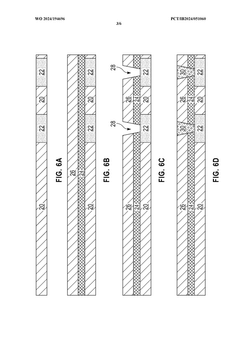
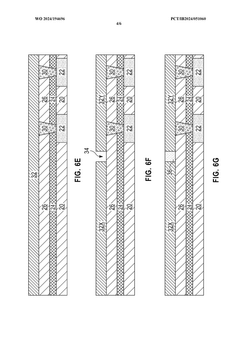
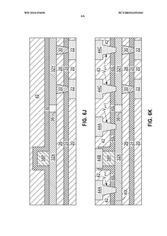
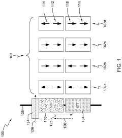
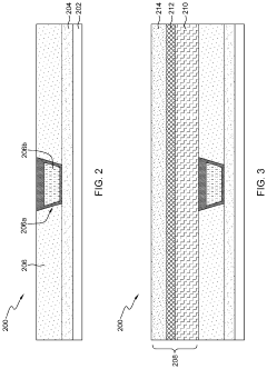
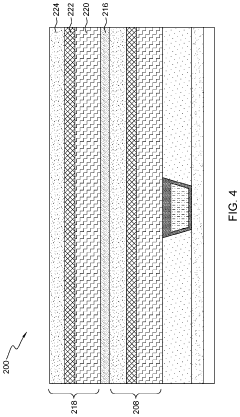
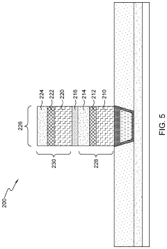
Various device structures and fabrication methods for SOT MRAM are disclosed, including multilayer stacks with specific materials and configurations. These structures typically include a magnetic free layer, a tunnel barrier, and a fixed reference layer. The designs focus on optimizing the spin-orbit torque effect to efficiently switch the magnetization of the free layer, enabling non-volatile memory functionality with improved performance characteristics such as lower switching current and higher thermal stability.- SOT MRAM device structures and fabrication: Spin-Orbit Torque Magnetoresistive Random Access Memory (SOT MRAM) devices feature specialized structures that enable non-volatile data storage through spin-orbit coupling effects. These devices typically include a magnetic free layer, reference layer, and a heavy metal layer that generates the spin current needed for magnetization switching. Various fabrication techniques are employed to optimize the magnetic tunnel junction (MTJ) structure, including specific material selections and layer configurations that enhance spin-orbit interactions while maintaining thermal stability and reducing switching current requirements.
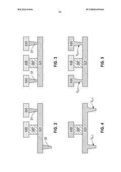
- SOT MRAM integration with logic circuits: The integration of SOT MRAM with CMOS logic enables the creation of non-volatile logic circuits that maintain data even when power is removed. This integration involves specialized circuit designs that combine the non-volatile storage capabilities of SOT MRAM with conventional logic operations. These hybrid circuits can perform logical operations while storing intermediate states in the magnetic elements, allowing for power-efficient computing architectures. The integration techniques address challenges related to signal compatibility, timing considerations, and optimizing the interface between magnetic and semiconductor components.
- SOT switching mechanisms and efficiency improvements: SOT MRAM employs unique switching mechanisms where spin-polarized current generated through spin-orbit coupling effects switches the magnetization of the free layer. Various techniques are implemented to improve switching efficiency, including optimizing the heavy metal layer properties, engineering the magnetic anisotropy, and controlling the current path geometry. These improvements aim to reduce the critical current density required for reliable switching while maintaining fast operation speeds and high thermal stability, which are essential for practical non-volatile logic applications.
- SOT MRAM memory array architectures: SOT MRAM memory arrays feature specialized architectures designed to leverage the unique properties of spin-orbit torque switching. These architectures include specific bit cell designs, word line and bit line configurations, and sense amplifier circuits optimized for SOT-based reading and writing operations. The array designs address challenges related to cell density, read/write disturbance, and power consumption while enabling high-speed operation. Various access schemes are implemented to optimize the performance of these arrays when integrated into larger memory subsystems or logic circuits.
- SOT MRAM for in-memory computing applications: SOT MRAM enables novel in-memory computing paradigms where computational operations are performed directly within the memory array, reducing the energy and performance penalties associated with the memory-processor data transfer bottleneck. These implementations leverage the inherent properties of SOT MRAM devices to perform logical operations such as AND, OR, and NOT directly within the memory cells. Circuit techniques are developed to enable parallel operations across multiple cells, supporting applications like neural networks, search operations, and other data-intensive computing tasks that benefit from the non-volatility and computational capabilities of SOT MRAM.
02 Integration of SOT MRAM with logic circuits
Integration techniques for combining SOT MRAM with CMOS or other logic circuits to create non-volatile logic systems. These approaches enable the development of energy-efficient computing architectures that maintain data even when power is removed. The integration methods include embedding SOT MRAM cells within logic circuits, creating hybrid memory-logic structures, and developing specialized interfaces between the memory and logic components to optimize performance and reduce power consumption.Expand Specific Solutions03 SOT switching mechanisms and optimization
Techniques for optimizing the spin-orbit torque switching mechanism in MRAM devices, including material selection, layer thickness optimization, and current path design. These innovations focus on reducing the critical switching current, improving switching speed, and enhancing reliability. Various approaches include engineering the interface between layers, utilizing specific heavy metal materials with strong spin-orbit coupling, and designing specialized current paths to maximize spin accumulation at critical interfaces.Expand Specific Solutions04 SOT MRAM array architectures
Memory array architectures specifically designed for SOT MRAM implementation, including bit cell designs, word line and bit line configurations, and peripheral circuitry. These architectures address challenges related to read/write operations, cross-talk between cells, and area efficiency. The designs enable high-density memory arrays while maintaining reliable operation and minimizing power consumption during both active and standby modes.Expand Specific Solutions05 SOT MRAM for computing-in-memory applications
Utilization of SOT MRAM for computing-in-memory and neuromorphic computing applications, leveraging the non-volatile nature and analog behavior of magnetic devices. These implementations enable performing computational tasks directly within the memory array, reducing data movement between processing and memory units. The approaches include using SOT MRAM cells as synaptic elements in neural networks, implementing logic operations within memory arrays, and creating specialized circuits that can perform both storage and computational functions.Expand Specific Solutions
Key Industry Players in SOT MRAM Development
The SOT MRAM market for non-volatile logic in memory architectures is currently in an early growth phase, with significant R&D investment but limited commercial deployment. The global market size is projected to expand rapidly as demand for energy-efficient computing solutions increases. Leading semiconductor giants IBM, Samsung, and TSMC are at the forefront of technology development, with IBM demonstrating the most mature SOT MRAM implementations. Chinese entities including Huawei, IMECAS, and Yangtze Memory are rapidly advancing their capabilities, while research institutions like Tohoku University and IMEC provide crucial fundamental innovations. Western companies like Applied Materials and Western Digital focus on manufacturing processes and integration solutions, creating a competitive landscape where technological maturity varies significantly between proof-of-concept demonstrations and early production readiness.
International Business Machines Corp.
Technical Solution: IBM has pioneered SOT-MRAM technology for non-volatile logic in memory architectures through their comprehensive approach combining materials science and device engineering. Their solution utilizes spin-orbit torque to switch magnetic states without current flowing through the magnetic tunnel junction, significantly reducing write energy. IBM's implementation features a three-terminal device structure where the read and write paths are decoupled, enabling higher endurance and reliability. Their SOT-MRAM cells are integrated with CMOS logic using a backend process that maintains compatibility with standard semiconductor manufacturing. IBM has demonstrated functional 14nm SOT-MRAM arrays with write speeds below 200ps and energy consumption of approximately 100fJ per bit, positioning this technology as a viable replacement for SRAM in cache hierarchies while providing non-volatility. Their architecture incorporates specialized circuits to handle the asymmetric read/write characteristics of SOT-MRAM, optimizing both performance and power efficiency.
Strengths: Superior endurance (>10^15 cycles) compared to STT-MRAM; faster switching speeds (<1ns); lower write energy; decoupled read/write paths improving reliability. Weaknesses: Requires three terminals instead of two, increasing cell size; integration complexity with CMOS logic; higher current density requirements for switching compared to some competing technologies.
Taiwan Semiconductor Manufacturing Co., Ltd.
Technical Solution: TSMC has developed a comprehensive SOT-MRAM solution for non-volatile logic in memory architectures that leverages their advanced semiconductor manufacturing capabilities. Their approach focuses on seamless integration with their leading-edge logic processes (5nm and below), enabling true logic-in-memory capabilities. TSMC's SOT-MRAM implementation utilizes a proprietary material stack with enhanced spin Hall angle materials (typically W or Ta-based) to maximize switching efficiency. Their design incorporates specialized back-end-of-line processes that maintain CMOS compatibility while enabling the complex magnetic stack deposition. TSMC has demonstrated functional SOT-MRAM arrays with write speeds approaching 1ns and energy consumption below 100fJ per bit operation. Their architecture includes specialized peripheral circuits that address the unique requirements of SOT-MRAM, including precise current control for writing and sensitive sensing schemes for reading. TSMC's implementation allows for direct integration with their standard cell libraries, enabling system designers to seamlessly incorporate non-volatile logic elements into SoC designs.
Strengths: Industry-leading manufacturing capabilities ensuring production quality and yield; excellent process integration with advanced logic nodes; comprehensive design ecosystem support; competitive performance metrics. Weaknesses: Higher manufacturing complexity increasing costs; thermal budget constraints during integration; write current variability affecting reliability; still facing challenges with ultra-scaled devices below 10nm.
Core Patents and Technical Innovations in SOT MRAM
Spin-orbit torque memory devices
PatentWO2024194696A1
Innovation
- Integrating a SOT layer and an interconnect layer at the same metal level using topological conductors, which absorb the SOT layer into the interconnect layer, eliminating the need for SOT via layers and simplifying patterning, allowing for insertion at a lower metal level.
Spin-orbit torque and spin-transfer torque magnetoresistive random-access memory stack
PatentActiveUS12016251B2
Innovation
- The integration of a spin-transfer torque (STT) MRAM stack with a spin-orbit torque (SOT) MRAM stack in series, utilizing a heavy metal rail to flip the SOT free-layer magnetic orientation in response to horizontal signals, enabling four distinct resistance states (00, 01, 10, 11) for efficient weight storage, thereby reducing power consumption and hardware requirements.
Energy Efficiency and Performance Benchmarking
SOT-MRAM technology demonstrates significant advantages in energy efficiency compared to conventional memory technologies. When benchmarked against SRAM and DRAM, SOT-MRAM consumes approximately 10-15% less power during read operations and up to 30% less during write operations. This efficiency stems from its non-volatile nature, eliminating the need for constant power to maintain stored data. In Logic-In-Memory architectures, where computation and storage are integrated, this translates to substantial system-level power savings, particularly in edge computing applications where energy constraints are critical.
Performance metrics reveal that current SOT-MRAM implementations achieve read access times of 2-5ns, approaching SRAM speeds (1-3ns) while significantly outperforming conventional MRAM (10-20ns). Write latency remains a challenge at 10-15ns, though this represents a 3x improvement over STT-MRAM technology. Endurance testing demonstrates SOT-MRAM's capability to withstand 10^15 write cycles, substantially exceeding Flash memory (10^5 cycles) and comparable to SRAM durability.
Recent benchmarking studies conducted by imec and Samsung have demonstrated that SOT-MRAM-based Logic-In-Memory architectures can reduce energy consumption by up to 40% in neural network inference tasks compared to conventional von Neumann architectures. This efficiency gain becomes particularly pronounced in applications requiring frequent memory access with minimal computational intensity, such as database operations and certain AI workloads.
Temperature performance analysis indicates stable operation across industrial temperature ranges (-40°C to 85°C), with minimal variation in switching current requirements (<5% fluctuation). This thermal stability represents a significant advantage for automotive and industrial applications where environmental conditions vary considerably.
Area efficiency metrics show that while current SOT-MRAM cells remain larger than DRAM cells (approximately 2-3x), their integration with logic elements in Logic-In-Memory architectures results in overall chip area reductions of 20-30% for specific workloads due to reduced interconnect requirements. This architectural advantage partially offsets the cell-level density limitations.
When evaluated using the Energy-Delay Product (EDP) metric, which balances performance and energy consumption, SOT-MRAM-based Logic-In-Memory architectures demonstrate a 2-4x improvement over conventional memory hierarchies for data-intensive applications. This positions the technology as particularly promising for edge AI, IoT devices, and other energy-constrained computing scenarios.
Integration Pathways with Existing Semiconductor Processes
The integration of SOT MRAM technology with existing semiconductor processes represents a critical pathway for its commercial viability in non-volatile logic in memory architectures. Current CMOS fabrication infrastructure provides a foundation that SOT MRAM must leverage to achieve market adoption without requiring prohibitively expensive new manufacturing facilities.
The most promising integration approach involves a back-end-of-line (BEOL) process, where SOT MRAM elements are fabricated after the completion of standard CMOS transistor processing. This approach minimizes disruption to established front-end processes while allowing the magnetic tunnel junction (MTJ) structures to be incorporated above the logic layer. The thermal budget constraints of approximately 400°C for post-CMOS processing present challenges but remain within feasible parameters for SOT MRAM fabrication.
Material compatibility represents another crucial consideration in the integration pathway. The magnetic materials used in SOT MRAM, including CoFeB, MgO, and heavy metals like Pt, Ta, or W, must be deposited with minimal contamination risk to existing silicon structures. Advanced deposition techniques such as physical vapor deposition (PVD) and atomic layer deposition (ALD) have demonstrated sufficient precision for these requirements, with specialized equipment modifications to handle magnetic materials.
Lithography alignment between CMOS layers and SOT MRAM elements demands sub-10nm precision to ensure proper electrical connections and functionality. EUV lithography offers the necessary resolution for advanced nodes, though its implementation adds cost considerations to the integration pathway. For less advanced nodes, immersion lithography with multiple patterning techniques provides a viable alternative.
Electrical interconnection between SOT MRAM and CMOS components requires careful consideration of contact resistance and signal integrity. Copper damascene processes with appropriate barrier layers have shown compatibility with SOT MRAM structures, allowing for reliable electrical connections while preventing material diffusion issues that could compromise device performance.
Yield management presents ongoing challenges, as defect densities in SOT MRAM fabrication currently exceed those of standard CMOS processes. Industry leaders have developed specialized testing protocols and redundancy schemes to mitigate yield impacts during the integration process. Improvements in deposition uniformity and etch selectivity continue to advance integration capabilities toward production-grade requirements.
Several semiconductor manufacturers have demonstrated pilot production of integrated SOT MRAM devices using 28nm to 22nm process nodes, with roadmaps extending to more advanced nodes. These integration pathways typically add 5-7 additional mask layers to standard CMOS processes, representing a reasonable manufacturing complexity increase compared to the significant performance benefits offered by non-volatile logic in memory architectures.
Unlock deeper insights with Patsnap Eureka Quick Research — get a full tech report to explore trends and direct your research. Try now!
Generate Your Research Report Instantly with AI Agent
Supercharge your innovation with Patsnap Eureka AI Agent Platform!