Back End Of Line Integration Challenges For SOT MRAM
AUG 28, 20259 MIN READ
Generate Your Research Report Instantly with AI Agent
Patsnap Eureka helps you evaluate technical feasibility & market potential.
SOT MRAM BEOL Integration Background and Objectives
Spin-Orbit Torque Magnetic Random Access Memory (SOT MRAM) has emerged as a promising next-generation non-volatile memory technology, offering advantages in speed, endurance, and power efficiency compared to conventional memory solutions. The evolution of SOT MRAM technology represents a significant advancement from earlier MRAM variants, including Toggle MRAM and Spin-Transfer Torque (STT) MRAM, with each iteration addressing specific limitations of its predecessors.
The development of SOT MRAM technology can be traced back to fundamental research in spintronics during the early 2000s, with significant breakthroughs in understanding spin-orbit interactions in magnetic materials. By 2010, researchers had begun exploring the potential of spin-orbit torques for manipulating magnetic states, laying the groundwork for SOT MRAM concepts. The technology has since progressed through various stages of development, moving from theoretical concepts to experimental demonstrations and now approaching commercial viability.
The primary technical objective for SOT MRAM is to achieve successful Back End Of Line (BEOL) integration while maintaining device performance and reliability. BEOL integration refers to the process of incorporating SOT MRAM elements into the interconnect layers of semiconductor devices, which presents significant challenges due to material compatibility issues, thermal budget constraints, and process integration complexities.
Current technical goals include developing BEOL-compatible materials and processes that can withstand temperatures up to 400°C without degradation of magnetic properties, reducing critical current densities for switching while maintaining thermal stability, and ensuring reliable operation over extended cycling. Additionally, there is a focus on scaling SOT MRAM devices to sub-20nm dimensions to compete with existing memory technologies in terms of density and cost.
The technology trajectory indicates a continued evolution toward higher performance, with research efforts concentrated on novel materials such as topological insulators and 2D materials that could potentially enhance spin-orbit coupling efficiency. Concurrently, there is significant interest in developing innovative device architectures that can leverage the unique advantages of SOT switching while mitigating integration challenges.
The successful realization of BEOL-integrated SOT MRAM could enable a new generation of energy-efficient computing architectures, including in-memory computing and neuromorphic systems. This technology is positioned to address the growing demand for fast, non-volatile memory solutions in applications ranging from IoT devices to data center storage, making it a critical area for continued research and development investment.
Market Analysis for SOT MRAM Technologies
The global market for SOT-MRAM (Spin-Orbit Torque Magnetic Random Access Memory) technologies is experiencing significant growth, driven by increasing demand for non-volatile memory solutions with enhanced performance characteristics. Current market projections indicate that the overall MRAM market, of which SOT-MRAM represents an emerging segment, is expected to reach approximately $5 billion by 2028, with a compound annual growth rate exceeding 25% from 2023 to 2028.
The demand for SOT-MRAM is primarily fueled by its potential advantages over conventional memory technologies, including unlimited endurance, fast switching speeds, and compatibility with standard CMOS processes. These characteristics make SOT-MRAM particularly attractive for applications requiring both high performance and non-volatility, such as enterprise storage systems, automotive electronics, industrial automation, and edge computing devices.
Market segmentation analysis reveals that data centers and enterprise storage represent the largest current market opportunity for SOT-MRAM technologies, accounting for approximately 40% of potential applications. This is followed by automotive electronics (25%), industrial IoT devices (20%), and consumer electronics (15%). The automotive sector in particular shows promising growth potential due to increasing electronic content in vehicles and stringent reliability requirements.
Geographically, North America currently leads the market development for SOT-MRAM technologies, hosting major research institutions and semiconductor companies focused on MRAM advancement. Asia-Pacific, particularly Taiwan, South Korea, and Japan, represents the fastest-growing region due to the concentration of semiconductor manufacturing facilities and increasing investments in memory technologies.
Key market drivers include the growing data processing requirements of AI and machine learning applications, which demand faster and more energy-efficient memory solutions. Additionally, the expansion of edge computing and IoT deployments is creating demand for non-volatile memory with improved power efficiency and reliability in diverse environmental conditions.
Market barriers primarily relate to the technical challenges of BEOL integration for SOT-MRAM, which directly impact manufacturing costs and yield rates. The complexity of integrating magnetic materials with conventional CMOS processes represents a significant hurdle to widespread commercial adoption. Current manufacturing costs for SOT-MRAM remain substantially higher than established memory technologies like DRAM and NAND flash.
Customer adoption analysis indicates that enterprise and industrial sectors show the highest willingness to pay premium prices for SOT-MRAM's performance benefits, while consumer markets remain more price-sensitive. This suggests a market entry strategy focused initially on high-value applications where performance advantages outweigh cost considerations.
Technical Barriers in BEOL Integration for SOT MRAM
The integration of Spin-Orbit Torque Magnetic Random Access Memory (SOT MRAM) into the Back End Of Line (BEOL) process presents significant technical challenges that must be overcome for successful commercialization. These barriers stem from the complex material requirements and process compatibility issues inherent to SOT MRAM technology.
A primary challenge lies in the thermal budget constraints during BEOL processing. SOT MRAM requires high-quality magnetic materials and interfaces that can be degraded at temperatures above 400°C. However, standard BEOL processes often involve temperature excursions that exceed this threshold, potentially compromising the magnetic properties and performance of SOT MRAM devices.
Material compatibility issues represent another significant barrier. The heavy metals (such as Pt, W, or Ta) used for SOT generation must maintain clean interfaces with magnetic layers to ensure efficient spin current injection. Contamination or interdiffusion between these layers can severely degrade device performance. Additionally, these materials must be compatible with surrounding dielectrics and metal interconnects in the BEOL stack.
Etching processes present particular difficulties for SOT MRAM integration. The multi-material stacks containing heavy metals, magnetic materials, and tunnel barriers require highly selective etching techniques that can precisely pattern these structures without causing sidewall damage or redeposition that could lead to device shorting or performance degradation.
Dimensional scaling represents a critical barrier as well. As device dimensions shrink below 30nm, maintaining the thermal stability of the magnetic free layer while ensuring sufficient SOT efficiency becomes increasingly challenging. The reduced volume of magnetic material must still retain sufficient energy barriers to prevent spontaneous magnetization switching due to thermal fluctuations.
Uniformity and yield concerns also plague SOT MRAM BEOL integration. The complex multi-layer stacks must be deposited with exceptional uniformity across the wafer to ensure consistent device performance. Even minor variations in layer thickness or interface quality can lead to significant device-to-device variability, hampering manufacturing yield.
Reliability testing frameworks for SOT MRAM integrated into BEOL are still evolving. Understanding failure mechanisms, developing appropriate accelerated testing methodologies, and establishing reliability models remain works in progress. This uncertainty creates barriers for adoption in critical applications where long-term reliability is paramount.
Finally, the integration of SOT MRAM with CMOS periphery circuits presents challenges in terms of parasitic effects, signal integrity, and overall system performance. The additional processing steps required for SOT MRAM integration must not compromise the performance of existing CMOS devices or interconnects.
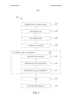
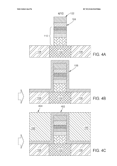
Current BEOL Integration Approaches for SOT MRAM
01 SOT MRAM device structure and fabrication
SOT MRAM devices utilize spin-orbit torque to switch the magnetization of the free layer in the magnetic tunnel junction (MTJ). The fabrication process involves depositing multiple layers including a magnetic free layer, tunnel barrier, and reference layer. The structure typically includes a heavy metal layer that generates the spin current necessary for switching. These devices offer advantages such as lower switching current and higher endurance compared to conventional STT-MRAM.- SOT MRAM device structure and fabrication: SOT MRAM devices incorporate specific structural elements that enable spin-orbit torque switching. These structures typically include magnetic tunnel junctions (MTJs) with perpendicular magnetic anisotropy, heavy metal layers for spin current generation, and specialized electrode configurations. The fabrication process involves precise deposition of multiple thin film layers including ferromagnetic materials, tunnel barriers, and heavy metal layers that generate the spin-orbit torque effect. These structural innovations are critical for achieving efficient switching and reliable operation of SOT MRAM devices.
- BEOL integration techniques for SOT MRAM: Back-End-Of-Line integration of SOT MRAM involves specialized processes to incorporate memory elements into the interconnect layers of semiconductor devices. This includes developing compatible etching processes, thermal budgets, and metallization schemes that preserve the magnetic properties of the memory elements. Integration challenges include managing thermal stability during subsequent processing steps, ensuring proper electrical connections to the memory array, and maintaining the integrity of the magnetic materials throughout the fabrication process. These techniques enable SOT MRAM to be embedded within standard CMOS process flows.
- SOT MRAM cell design and array architecture: SOT MRAM cell designs focus on optimizing the memory density, access speed, and power consumption. Various cell architectures have been developed, including 2T-1MTJ (two transistors, one magnetic tunnel junction) and 1T-1MTJ configurations. Array architectures address challenges in addressing, sensing, and controlling write currents for reliable operation. Advanced designs incorporate innovations in bit line and word line arrangements to minimize cross-talk and improve read/write margins. These architectural approaches are essential for scaling SOT MRAM technology to higher densities while maintaining performance advantages.
- Materials engineering for SOT MRAM: Materials engineering is crucial for SOT MRAM performance, focusing on developing materials with enhanced spin-orbit coupling, thermal stability, and magnetoresistance ratios. Heavy metals like tungsten, platinum, and tantalum are optimized for efficient spin current generation. Magnetic materials are engineered for appropriate coercivity and switching characteristics. Interface engineering between layers is critical for maintaining spin polarization and reducing defects. Advanced material stacks may incorporate synthetic antiferromagnets, perpendicular magnetic anisotropy materials, and specialized capping layers to improve reliability and endurance of the memory devices.
- SOT MRAM reliability and performance optimization: Reliability and performance optimization for SOT MRAM focuses on addressing challenges such as read disturbance, write errors, and data retention. Techniques include developing specialized sensing circuits, optimizing write current paths to reduce power consumption, and implementing error correction schemes. Performance enhancements involve reducing switching current density, improving thermal stability, and increasing magnetoresistance ratios. Advanced designs incorporate strategies to mitigate process variations and ensure consistent operation across a wide temperature range. These optimizations are essential for enabling SOT MRAM to meet the requirements for both embedded and standalone memory applications.
02 Back-end-of-line integration techniques
Integration of SOT MRAM into the back-end-of-line (BEOL) process involves specific techniques to ensure compatibility with existing CMOS fabrication. This includes precise alignment of the MTJ stack with underlying CMOS circuitry, development of specialized etching processes that don't damage the magnetic materials, and implementation of thermal budgets that preserve the magnetic properties of the materials during subsequent processing steps. BEOL integration enables the creation of embedded memory solutions that can be manufactured using standard semiconductor processes.Expand Specific Solutions03 Materials engineering for SOT MRAM
Advanced materials are crucial for SOT MRAM performance. Heavy metals like tungsten, platinum, or tantalum are used for the spin-orbit coupling layer to generate efficient spin currents. The magnetic free layer typically consists of CoFeB or similar ferromagnetic materials with perpendicular magnetic anisotropy. The tunnel barrier is usually made of MgO for high tunnel magnetoresistance ratio. Material selection and engineering focus on optimizing spin-orbit coupling efficiency, thermal stability, and switching reliability while maintaining CMOS compatibility.Expand Specific Solutions04 Circuit design and memory array architecture
SOT MRAM memory arrays require specialized circuit designs to efficiently write and read data. The write operation utilizes current through the heavy metal layer rather than through the MTJ itself, which requires unique transistor configurations and bit/word line arrangements. Read operations measure the resistance of the MTJ to determine the stored state. The memory array architecture must address challenges such as sneak current paths, sense amplifier design, and write driver circuits while maintaining density and performance comparable to other memory technologies.Expand Specific Solutions05 Reliability and manufacturing considerations
Ensuring reliability of SOT MRAM during manufacturing and operation involves addressing several challenges. These include process variation control during fabrication, prevention of edge damage during MTJ patterning, management of thermal stability to prevent data loss, and development of testing methodologies specific to SOT MRAM. Manufacturing considerations also include yield improvement techniques, defect detection methods, and implementation of redundancy schemes to enhance production efficiency and device reliability in commercial applications.Expand Specific Solutions
Key Industry Players in SOT MRAM Development
The Back End Of Line (BEOL) integration challenges for SOT MRAM technology are currently at a critical development stage, with the market showing promising growth potential despite being in its early commercialization phase. Major semiconductor players including IBM, TSMC, Samsung, and Applied Materials are leading technological advancements, while research institutions like IMEC and universities such as Zhejiang University and National Taiwan University contribute significant innovations. The technology is approaching maturity with key challenges in scalability, thermal stability, and manufacturing integration being addressed through collaborative efforts. Chinese entities including Huawei and SMIC are increasingly investing in this space, indicating the strategic importance of SOT MRAM in future memory solutions for AI, IoT, and automotive applications.
International Business Machines Corp.
Technical Solution: IBM has developed advanced SOT MRAM integration solutions focusing on the critical BEOL challenges. Their approach involves a unique dual damascene process for SOT MRAM integration that addresses thermal budget limitations. IBM's technology utilizes tungsten contacts and specialized barrier layers to prevent metal diffusion during high-temperature processes. They've implemented a multi-step etching process for precise magnetic tunnel junction (MTJ) formation with minimal sidewall damage, crucial for device performance. IBM has also pioneered low-temperature deposition techniques for magnetic materials that maintain CMOS compatibility while ensuring high tunnel magnetoresistance ratios. Their integration scheme incorporates specialized capping layers and optimized annealing processes to enhance magnetic properties without compromising BEOL integrity.
Strengths: Industry-leading expertise in magnetic materials and MRAM technology; extensive patent portfolio; proven track record in commercializing memory technologies. Weaknesses: Complex manufacturing processes may increase production costs; thermal budget constraints still limit some integration options.
Taiwan Semiconductor Manufacturing Co., Ltd.
Technical Solution: TSMC has developed a sophisticated SOT MRAM BEOL integration platform addressing thermal budget constraints through innovative process engineering. Their approach utilizes a modified damascene process with specialized low-temperature deposition techniques for magnetic materials, maintaining temperatures below 350°C to preserve BEOL integrity. TSMC's solution incorporates advanced barrier layers using TaN/Ta combinations to prevent metal diffusion while maintaining electrical performance. They've implemented precise etching techniques using multi-step processes with specialized chemistries to achieve clean MTJ profiles with minimal sidewall redeposition. TSMC's integration scheme also features optimized encapsulation layers that protect magnetic elements during subsequent processing while providing necessary mechanical support. Their platform includes specialized CMP processes for planarization after MTJ formation, ensuring proper electrical contact without damaging the sensitive magnetic structures.
Strengths: World-leading semiconductor manufacturing expertise; advanced node capabilities; extensive experience with heterogeneous integration. Weaknesses: Less historical focus on magnetic materials compared to logic processes; challenges with material compatibility at most advanced nodes.
Critical Patents and Research in SOT MRAM Integration
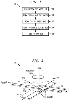
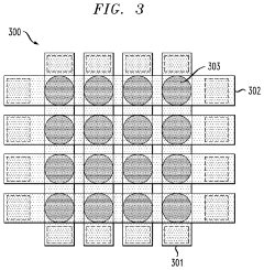
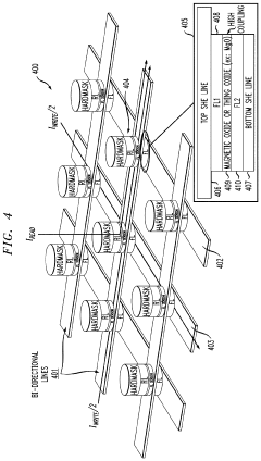
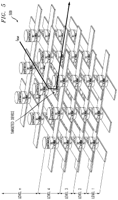
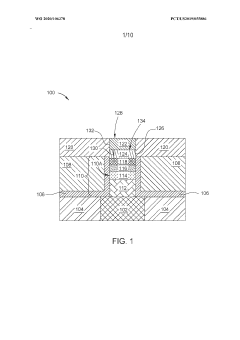
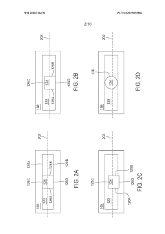
Spin orbit-torque magnetic random-access memory (sot-MRAM) with cross-point spin hall effect (SHE) write lines and remote sensing read magnetic tunnel-junction (MTJ)
PatentActiveUS20230086181A1
Innovation
- A cross-point SOT-MRAM cell design is implemented, featuring a first and second Spin Hall Effect (SHE) write line that are non-colinear, a cross-point free layer with dielectric isolation, and a remote sensing Magnetic Tunnel Junction (MTJ) to enable independent write and read operations without the need for STT-assisted writing, allowing for true cross-point architecture and improved integration density.
Spin orbit torque MRAM and manufacture thereof
PatentWO2020106378A1
Innovation
- The SOT-MRAM devices are fabricated with a bottom-pinned structure where the MTJ stack and SOT layer are formed in-situ without breaking vacuum, creating a high-quality interface and using an encapsulation layer to protect the free layer, with metal lines electrically coupling to the SOT layer on multiple sides to prevent current loss.
Material Science Advancements for SOT MRAM
Material science advancements have been pivotal in addressing the integration challenges for Spin-Orbit Torque Magnetic Random Access Memory (SOT MRAM) in the Back End Of Line (BEOL) processes. Recent breakthroughs in material engineering have significantly improved the thermal stability and switching efficiency of SOT MRAM devices, making them more compatible with standard CMOS fabrication processes.
The development of novel heavy metal materials with enhanced spin-orbit coupling properties has been a critical advancement. Materials such as tungsten (W), platinum (Pt), and tantalum (Ta) have demonstrated superior spin Hall angles, which directly correlates with improved switching efficiency. Particularly, beta-phase tungsten has shown exceptional promise due to its large spin Hall angle and compatibility with existing semiconductor manufacturing processes.
Researchers have also made significant progress in engineering the magnetic free layer materials. The traditional CoFeB-based free layers have been enhanced through precise control of crystalline anisotropy and interface engineering. The incorporation of synthetic antiferromagnetic (SAF) structures has further improved thermal stability while maintaining low switching currents, addressing one of the fundamental challenges in BEOL integration.
Interface engineering between the heavy metal and ferromagnetic layers has emerged as another crucial area of advancement. By optimizing the interface quality through techniques such as ion beam sputtering and post-deposition annealing, researchers have achieved better spin current transmission efficiency and reduced interfacial defects that can degrade device performance.
The development of novel capping layers and diffusion barriers has addressed the thermal budget constraints in BEOL processes. Materials such as MgO, TaN, and HfO2 have demonstrated excellent barrier properties against diffusion during high-temperature processing steps, preserving the integrity of the magnetic stack structure.
Recent advancements in atomic layer deposition (ALD) and chemical vapor deposition (CVD) techniques have enabled the precise control of ultra-thin film deposition required for SOT MRAM structures. These techniques allow for conformal coating with atomic-level precision, which is essential for maintaining consistent device performance across the wafer.
The exploration of alternative magnetic materials, including Heusler alloys and perpendicular magnetic anisotropy (PMA) materials, has opened new possibilities for SOT MRAM integration. These materials offer improved thermal stability and switching characteristics at reduced dimensions, making them promising candidates for advanced technology nodes where thermal budget constraints are more severe.
Scaling Challenges and Manufacturability Assessment
As SOT-MRAM technology advances toward commercial viability, scaling challenges present significant hurdles for mass production. The critical dimension scaling of SOT-MRAM devices faces fundamental physical limitations when approaching sub-20nm nodes. The write current density increases dramatically at smaller dimensions, creating thermal management issues that can compromise data retention and device reliability. Additionally, the magnetic tunnel junction (MTJ) stack becomes increasingly susceptible to process-induced damage during scaling.
Manufacturing SOT-MRAM at advanced nodes requires precise control of material deposition processes. The uniformity of ultra-thin layers (often <1nm) across 300mm wafers presents a major challenge, with even minor thickness variations significantly impacting device performance. The industry currently struggles to achieve the required ±2% thickness uniformity for critical magnetic layers in high-volume manufacturing environments.
Etching processes for SOT-MRAM present another significant manufacturability concern. The complex MTJ stack contains multiple materials with different etching characteristics, making it difficult to achieve clean, vertical profiles without redeposition or sidewall damage. Ion beam etching, commonly used for MTJ patterning, faces limitations in maintaining critical dimensions and avoiding sidewall redeposition at smaller nodes.
Integration with standard CMOS BEOL processes introduces additional challenges. The thermal budget constraints of SOT-MRAM (typically <400°C) limit the available process options for subsequent metallization and dielectric deposition steps. The introduction of new materials into established CMOS fabrication lines also raises contamination concerns, particularly regarding magnetic material migration that could affect adjacent devices.
Yield management represents perhaps the most pressing manufacturability challenge. Defect detection and classification for SOT-MRAM requires specialized metrology tools capable of identifying nanoscale magnetic defects that may not be visible through conventional inspection methods. Current in-line testing capabilities are insufficient for detecting subtle magnetic property variations that can cause device failures.
Cost-effective scaling will require innovations in materials engineering, process integration, and testing methodologies. The development of more efficient SOT materials with lower critical switching currents would alleviate many scaling challenges, while advances in deposition and etching technologies specifically optimized for magnetic materials could improve manufacturability at advanced nodes.
Unlock deeper insights with Patsnap Eureka Quick Research — get a full tech report to explore trends and direct your research. Try now!
Generate Your Research Report Instantly with AI Agent
Supercharge your innovation with Patsnap Eureka AI Agent Platform!