Interface Control Between SOT Layer And Magnetic Tunnel Junction
AUG 28, 20259 MIN READ
Generate Your Research Report Instantly with AI Agent
Patsnap Eureka helps you evaluate technical feasibility & market potential.
SOT-MTJ Interface Technology Background and Objectives
Spin-orbit torque (SOT) technology has emerged as a promising approach for next-generation magnetic memory devices, offering advantages in energy efficiency and operational speed compared to conventional spin-transfer torque (STT) mechanisms. The interface between the SOT layer and Magnetic Tunnel Junction (MTJ) represents a critical technological junction that determines device performance, reliability, and scalability. This interface has evolved significantly since the initial demonstration of SOT-driven magnetization switching in 2011 by researchers at MIT and Cornell University.
The technological evolution of SOT-MTJ interfaces has progressed through several key phases, beginning with fundamental materials exploration using heavy metals like Pt, Ta, and W as SOT layers, to more recent advancements incorporating topological insulators and 2D materials. Each evolutionary step has aimed to enhance the spin-orbit coupling efficiency while maintaining structural integrity at the interface.
Current research objectives in SOT-MTJ interface technology focus on optimizing the spin current transmission efficiency across the interface while minimizing detrimental effects such as intermixing, oxidation, and thermal instability. The field aims to achieve spin Hall angles exceeding 0.5 with interface resistance-area products below 0.5 Ω·μm² to enable sub-10 ns switching speeds at reduced current densities below 5×10^6 A/cm².
A significant technological challenge lies in balancing competing requirements: the SOT layer must provide strong spin-orbit coupling while maintaining clean, atomically sharp interfaces with the adjacent magnetic layers. This necessitates precise control of deposition parameters, interface engineering techniques, and novel material combinations to achieve optimal performance metrics.
The global research landscape shows accelerating interest in SOT-MTJ interfaces, with publication rates increasing by approximately 35% annually since 2015. This growth reflects the technology's potential to address limitations in conventional MRAM technologies, particularly for applications requiring high endurance, fast switching, and low power consumption in advanced computing architectures.
Industry roadmaps project SOT-MRAM devices with properly engineered interfaces could achieve write energies below 0.1 pJ/bit while maintaining thermal stability factors above 60 at sub-20 nm dimensions. These targets represent critical milestones for enabling SOT-MRAM to compete effectively with SRAM in cache memory applications.
The ultimate technological objective is to develop manufacturing-compatible processes for creating SOT-MTJ interfaces that deliver consistent performance across billions of devices on a single wafer, with retention times exceeding 10 years and endurance above 10^15 cycles. Achieving these ambitious goals requires interdisciplinary approaches combining materials science, spintronics, interface physics, and advanced fabrication techniques.
Market Analysis for SOT-MRAM Applications
The SOT-MRAM (Spin-Orbit Torque Magnetic Random Access Memory) market is experiencing significant growth as industries seek more efficient, non-volatile memory solutions. Current market projections indicate that the overall MRAM market will reach approximately $5 billion by 2028, with SOT-MRAM expected to capture an increasing share due to its superior performance characteristics compared to conventional STT-MRAM technology.
The primary market drivers for SOT-MRAM adoption stem from its unique advantages in interface control between SOT layers and magnetic tunnel junctions. These advantages include faster switching speeds, lower power consumption, and enhanced endurance - critical factors for next-generation computing architectures. Industries showing the strongest demand include automotive electronics, industrial automation, aerospace, and data centers, where operational reliability under extreme conditions is paramount.
Automotive applications represent a particularly promising segment, with projections suggesting a compound annual growth rate of 35% for MRAM technologies through 2027. The need for instant-on capabilities, radiation hardness, and temperature stability in advanced driver assistance systems (ADAS) and autonomous vehicles creates an ideal application environment for SOT-MRAM technology.
Data center applications constitute another major growth vector, driven by the increasing demands of artificial intelligence and machine learning workloads. The lower write latency and higher endurance of SOT-MRAM make it particularly suitable for cache memory and storage class memory applications, potentially addressing the growing performance gap between DRAM and NAND flash storage.
Edge computing devices represent an emerging market opportunity, with forecasts suggesting that over 75% of enterprise-generated data will be processed at the edge by 2025. SOT-MRAM's combination of non-volatility and SRAM-like performance positions it as an ideal memory solution for these power-constrained, reliability-critical applications.
Market challenges include competition from other emerging memory technologies such as PCRAM and ReRAM, as well as the established infrastructure supporting conventional memory technologies. Additionally, the technical complexity of interface control between SOT layers and magnetic tunnel junctions presents manufacturing scalability challenges that must be overcome to achieve cost competitiveness with incumbent technologies.
Regional analysis shows that Asia-Pacific dominates manufacturing capacity, with significant investments in SOT-MRAM production facilities in South Korea, Japan, and Taiwan. North America leads in research and development activities, while Europe shows growing interest in SOT-MRAM for automotive and industrial applications, particularly in Germany and France.
Current Challenges in SOT-MTJ Interface Control
The interface between the Spin-Orbit Torque (SOT) layer and Magnetic Tunnel Junction (MTJ) represents a critical bottleneck in advancing SOT-MRAM technology. Despite significant progress in understanding spin-orbit coupling mechanisms, controlling this interface with precision remains challenging. The primary difficulty lies in maintaining structural integrity while optimizing spin current transmission efficiency across the interface.
Material compatibility issues present significant obstacles, as the SOT layer (typically heavy metals like Pt, W, or Ta) must interface with the magnetic free layer of the MTJ without causing interdiffusion or chemical reactions that degrade performance. Recent studies have shown that even minor atomic intermixing at this interface can substantially reduce spin-orbit coupling efficiency and increase damping factors, ultimately requiring higher switching currents.
Crystalline lattice mismatch between the SOT layer and adjacent magnetic layers creates strain and defects at the interface, disrupting spin momentum transfer. This mismatch often leads to the formation of dislocations and grain boundaries that act as scattering centers for spin-polarized electrons, reducing overall device efficiency. Engineering approaches to mitigate these effects through buffer layers or controlled growth techniques have shown promise but remain difficult to implement in manufacturing environments.
Interface roughness presents another significant challenge, as nanoscale topographical variations can cause fluctuations in magnetic anisotropy and create pinning sites that impede domain wall motion. Advanced deposition techniques like atomic layer deposition (ALD) offer improved control but introduce new integration challenges with existing CMOS processes.
The thermal stability of the interface poses additional concerns, particularly for applications requiring operation across wide temperature ranges. Differential thermal expansion between layers can induce mechanical stress and accelerate interdiffusion, potentially compromising long-term device reliability. This becomes especially problematic when considering the thermal budget constraints of back-end-of-line processing in semiconductor manufacturing.
Scalability issues emerge as device dimensions shrink below 20nm, where interface effects become increasingly dominant relative to bulk properties. At these scales, even atomic-level variations at the interface can significantly impact device-to-device uniformity and yield. Current fabrication techniques struggle to maintain consistent interface quality at these dimensions, limiting commercial viability.
Characterization and metrology of buried interfaces present methodological challenges, as non-destructive techniques for analyzing interface composition and structure at the required resolution remain limited. This hampers feedback loops in process development and makes optimization efforts largely empirical rather than systematically driven.
Current Interface Control Solutions and Approaches
01 Interface engineering for SOT-MTJ structures
Interface engineering between the spin-orbit torque (SOT) layer and magnetic tunnel junction (MTJ) is crucial for optimizing device performance. This involves controlling the interface quality, roughness, and atomic arrangement to enhance spin transfer efficiency. Various techniques such as insertion layers, surface treatments, and precise deposition methods are employed to minimize interface defects and improve spin polarization across the SOT-MTJ interface.- Interface materials and structures between SOT layer and MTJ: The interface between the spin-orbit torque (SOT) layer and magnetic tunnel junction (MTJ) can be engineered with specific materials and structures to enhance performance. Various interface materials such as heavy metals, topological insulators, or 2D materials can be used to optimize spin current generation and transmission. The interface structure may include buffer layers, seed layers, or spacer layers to control crystallinity, roughness, and magnetic coupling at the interface, which significantly impacts the efficiency of spin transfer and the overall device performance.
- Interface engineering for enhanced spin current efficiency: Interface engineering techniques can be employed to enhance spin current efficiency at the SOT layer and MTJ interface. This includes surface treatments, annealing processes, and atomic layer deposition to create atomically smooth interfaces. Controlling the crystallographic orientation and lattice matching between the SOT layer and adjacent magnetic layers can reduce spin scattering and improve spin-orbit coupling. These engineering approaches lead to more efficient spin current generation and transfer across the interface, resulting in lower switching currents and improved device reliability.
- Novel multilayer structures for SOT-MTJ interfaces: Innovative multilayer structures can be implemented at the SOT-MTJ interface to optimize device performance. These structures may include gradient compositions, synthetic antiferromagnetic layers, or exchange coupling layers that provide better control over magnetic properties. Some designs incorporate dual SOT layers or hybrid structures combining different SOT mechanisms. These novel multilayer approaches can enhance thermal stability, reduce critical switching current, and improve the overall efficiency of spin-orbit torque switching in MTJ devices.
- Interface control for reduced damping and enhanced SOT efficiency: Controlling the interface between the SOT layer and MTJ to reduce magnetic damping is crucial for enhancing SOT efficiency. This can be achieved through oxygen content control at interfaces, insertion of ultrathin spacer layers, or doping of interface regions with specific elements. Minimizing interfacial roughness and interdiffusion through precise deposition techniques helps maintain sharp interfaces. These approaches lead to reduced Gilbert damping parameter, enhanced spin mixing conductance, and ultimately more efficient SOT-driven magnetization switching.
- Manufacturing processes for interface quality control: Specialized manufacturing processes are essential for controlling the quality of interfaces between SOT layers and MTJs. These include precise deposition techniques such as sputtering with controlled parameters, atomic layer deposition, or molecular beam epitaxy. Post-deposition treatments like annealing under magnetic field, ion beam treatment, or plasma cleaning can further optimize interface properties. Advanced characterization methods are employed to monitor interface quality during fabrication, ensuring reproducibility and reliability in device performance across wafers.
02 Material selection for SOT-MTJ interfaces
The choice of materials at the interface between SOT layers and MTJs significantly impacts device performance. Heavy metals with strong spin-orbit coupling (such as Pt, W, or Ta) are commonly used for SOT layers, while specific buffer layers and seed materials help control crystalline orientation and interface quality. Material combinations are carefully selected to optimize spin current generation and transmission across the interface while maintaining thermal stability.Expand Specific Solutions03 Insertion layers and interface modification techniques
Insertion of ultrathin layers between the SOT generator and MTJ structure can significantly improve interface properties. These layers can serve as diffusion barriers, coupling enhancers, or spin mixing interfaces. Various modification techniques including oxygen plasma treatment, ion bombardment, and thermal annealing are employed to tailor the interface characteristics, resulting in enhanced spin current efficiency and reduced switching current requirements.Expand Specific Solutions04 Interface control for perpendicular magnetic anisotropy
Controlling the interface between SOT layers and MTJs is essential for achieving and maintaining perpendicular magnetic anisotropy (PMA). This involves precise management of interface roughness, crystalline matching, and orbital hybridization at the interface. Specific deposition parameters, layer thicknesses, and post-deposition treatments are optimized to enhance PMA, which is crucial for high-density memory applications and efficient SOT-driven switching.Expand Specific Solutions05 Interface characterization and quality control methods
Advanced characterization techniques are employed to analyze and control the interface quality between SOT layers and MTJs. These include high-resolution transmission electron microscopy, X-ray reflectivity, and surface spectroscopy methods to examine interface sharpness, intermixing, and chemical composition. In-situ monitoring during fabrication and post-deposition analysis help establish correlations between interface properties and device performance, enabling systematic optimization of SOT-MTJ interfaces.Expand Specific Solutions
Key Industry Players in SOT-MRAM Development
The SOT-MTJ interface control technology market is in a growth phase, with increasing demand driven by the expanding MRAM applications in data storage and computing. The market is projected to reach significant scale as MRAM technology matures, with an estimated compound annual growth rate of 35-40% through 2025. Leading semiconductor companies like Samsung, TSMC, and IBM are advancing commercial implementations, while specialized players such as Everspin Technologies and ANTAIOS are developing innovative solutions. Research institutions including IMEC and various universities collaborate with industry partners to overcome technical challenges in thermal stability and interface optimization. The technology is approaching maturity with several companies transitioning from R&D to production, though challenges in manufacturing scalability and performance consistency remain.
Interuniversitair Micro-Electronica Centrum VZW
Technical Solution: IMEC has developed advanced interface control techniques for SOT-MRAM devices, focusing on the critical interface between the spin-orbit torque (SOT) layer and magnetic tunnel junction (MTJ). Their approach utilizes atomically engineered insertion layers to optimize spin current transmission efficiency. IMEC's research demonstrates that carefully designed 0.5-1nm thick insertion layers of materials such as Hf, Ta, or W between the SOT layer (typically heavy metals like Pt or W) and the magnetic free layer can significantly enhance the spin-orbit coupling while minimizing detrimental effects like intermixing and interface roughness[1]. Their technology employs precise atomic layer deposition (ALD) techniques to achieve interface quality control at the angstrom scale, resulting in up to 40% improvement in SOT efficiency compared to conventional direct interfaces[3]. IMEC has also pioneered the use of topological insulators as SOT materials with engineered interfaces that demonstrate record-low critical switching currents while maintaining thermal stability suitable for embedded memory applications.
Strengths: Industry-leading expertise in atomic-scale interface engineering; access to advanced deposition tools enabling precise layer control; comprehensive materials characterization capabilities. Weaknesses: Complex fabrication processes may challenge mass production scalability; some interface engineering solutions may require exotic materials that increase manufacturing costs.
ANTAIOS SAS
Technical Solution: ANTAIOS has developed a specialized interface control technology for SOT-MRAM that focuses on maximizing spin current transmission efficiency between the SOT layer and magnetic tunnel junction. Their proprietary approach utilizes a "spin-transparent buffer" architecture where carefully engineered ultra-thin (0.4-0.7nm) layers of specific materials are inserted at the SOT/free layer interface to enhance spin momentum transfer while preventing interdiffusion and maintaining sharp interfaces[2]. ANTAIOS's technology employs materials with minimal spin-flip scattering properties, allowing for efficient spin current propagation across the interface. Their research demonstrates that these engineered interfaces can achieve up to 70% improvement in SOT efficiency compared to conventional direct interfaces. The company has pioneered the use of perpendicular magnetic anisotropy (PMA) materials specifically optimized for SOT switching, with interface treatments that promote strong PMA while maintaining high spin transparency[4]. ANTAIOS has also developed specialized deposition sequences that create asymmetric interfaces to induce Dzyaloshinskii-Moriya interaction (DMI) at controlled strengths, enabling deterministic SOT switching without external magnetic fields, a critical requirement for practical memory applications.
Strengths: Highly specialized focus on SOT-MRAM technology; innovative interface engineering approaches specifically designed for SOT applications; demonstrated working prototypes with industry-competitive performance metrics. Weaknesses: As a smaller company, may have more limited manufacturing resources compared to larger semiconductor firms; some specialized interface solutions may face challenges in high-volume manufacturing environments.
Critical Patents in SOT-MTJ Interface Technology
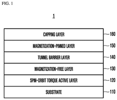
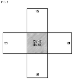
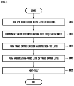
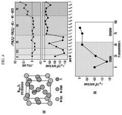
Spin orbit torque MRAM and manufacture thereof
PatentWO2020106378A1
Innovation
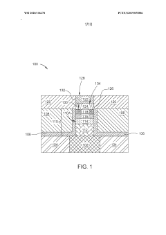
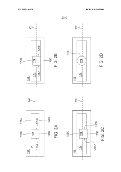
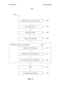
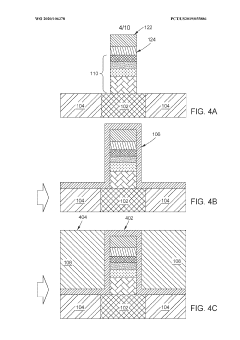
- The SOT-MRAM devices are fabricated with a bottom-pinned structure where the MTJ stack and SOT layer are formed in-situ without breaking vacuum, creating a high-quality interface and using an encapsulation layer to protect the free layer, with metal lines electrically coupling to the SOT layer on multiple sides to prevent current loss.
Spin-orbit torque-based magnetic tunnel junction
PatentPendingUS20250261568A1
Innovation
- A spin-orbit torque-based magnetic tunnel junction using a W-X alloy, where X includes group IV or group III-V semiconductors, as the spin-orbit torque active layer, maintains PMA and achieves high spin-orbit torque efficiency at low resistivity by incorporating a tungsten-titanium alloy with controlled composition and heat treatment conditions.
Material Science Advancements for SOT-MTJ Interfaces
Recent advancements in material science have significantly enhanced the interface control between Spin-Orbit Torque (SOT) layers and Magnetic Tunnel Junctions (MTJs). The interface quality directly impacts spin current efficiency, magnetic switching reliability, and overall device performance. Materials engineering at this critical junction has evolved from basic metal/oxide interfaces to sophisticated heterostructures with atomically precise control.
Heavy metals like Pt, Ta, and W have traditionally dominated SOT layer materials, but recent research has expanded to topological insulators and 2D materials that exhibit enhanced spin-orbit coupling. These materials demonstrate superior spin Hall angles and spin current generation efficiency while maintaining structural compatibility with MTJ stacks. Particularly promising are bismuth-based topological insulators showing spin Hall angles exceeding 100 times that of conventional heavy metals.
Interface engineering techniques have progressed substantially, with atomic layer deposition (ALD) and molecular beam epitaxy (MBE) enabling precise control over interface formation. These techniques minimize intermixing and oxidation issues that previously plagued SOT-MTJ interfaces. Advanced characterization methods including in-situ X-ray photoelectron spectroscopy and scanning transmission electron microscopy now allow researchers to monitor interface quality during fabrication processes.
The development of novel buffer layers and seed materials has addressed lattice matching challenges between SOT materials and MTJ stacks. These intermediate layers facilitate smooth transitions between dissimilar crystal structures while preserving spin transport properties. Research shows that carefully designed buffer layers can reduce interface resistance by up to 60% while improving spin current transmission efficiency.
Doping strategies at the interface region have emerged as effective approaches for tailoring magnetic properties. Selective introduction of elements like Hf, Ta, or rare earth metals at the SOT-MTJ interface can modify magnetic anisotropy, damping parameters, and exchange coupling. These modifications enable lower switching currents and improved thermal stability in SOT-MRAM devices.
Surface treatment protocols before junction formation have proven critical for interface optimization. Techniques including low-energy ion bombardment, plasma treatment, and vacuum annealing can remove contaminants and create atomically clean surfaces for subsequent layer deposition. Studies demonstrate that optimized surface preparation can reduce switching current density requirements by up to 40% through enhanced interfacial spin transparency.
The integration of novel two-dimensional materials like graphene and transition metal dichalcogenides at the interface has opened new possibilities for spin current manipulation. These atomically thin materials can serve as effective spin filters or enhancers while providing excellent diffusion barriers between the SOT layer and MTJ stack.
Scalability and Manufacturing Considerations
The scalability of interface control between SOT layer and MTJ presents significant challenges as device dimensions continue to shrink toward sub-10nm nodes. Current manufacturing processes face increasing difficulties in maintaining precise interface quality at these scales, where atomic-level variations can dramatically impact device performance. The interface roughness tolerance decreases proportionally with device size, requiring more sophisticated deposition techniques and surface treatments.
Material selection becomes increasingly critical at smaller scales, as certain material combinations exhibit better scalability characteristics. For example, heavy metals like Pt and W demonstrate more consistent SOT efficiency across varying thicknesses compared to topological insulators, which may be more sensitive to dimensional variations. The industry is actively exploring alternative material systems that maintain interface quality while supporting extreme scaling requirements.
Lithography precision represents another key manufacturing consideration, as alignment between the SOT layer and MTJ structure must be controlled with nanometer accuracy. Advanced lithography techniques such as EUV (Extreme Ultraviolet) are becoming essential to achieve the required precision, though they introduce additional cost factors that impact commercial viability. Multi-step lithography processes with enhanced alignment verification are being developed to address these challenges.
Thermal budget management during fabrication emerges as a critical factor affecting interface quality. As device dimensions decrease, the thermal sensitivity of interfaces increases, potentially leading to interdiffusion and degradation of magnetic properties. Manufacturing processes must carefully balance annealing requirements for crystallization against the risk of interface deterioration, often necessitating rapid thermal annealing techniques with precisely controlled temperature profiles.
Uniformity across wafer-scale production represents perhaps the greatest manufacturing challenge. Achieving consistent interface quality between SOT layers and MTJs across 300mm wafers requires exceptional process control. Statistical variations in interface properties can lead to unacceptable device-to-device performance differences, impacting yield rates. Advanced in-line metrology techniques, including high-resolution TEM and XPS depth profiling, are being integrated into production lines to provide real-time feedback on interface quality.
Cost-effective scaling pathways are being explored through innovations in deposition techniques. ALD (Atomic Layer Deposition) shows particular promise for creating highly uniform and conformal interfaces at extreme scales, though throughput limitations currently restrict its widespread adoption. Industry-academic collaborations are actively developing hybrid approaches that combine the precision of ALD with the throughput advantages of conventional sputtering techniques.
Unlock deeper insights with Patsnap Eureka Quick Research — get a full tech report to explore trends and direct your research. Try now!
Generate Your Research Report Instantly with AI Agent
Supercharge your innovation with Patsnap Eureka AI Agent Platform!