Defect Tolerance And ECC Strategies For SOT MRAM Arrays
AUG 28, 20259 MIN READ
Generate Your Research Report Instantly with AI Agent
Patsnap Eureka helps you evaluate technical feasibility & market potential.
SOT MRAM Technology Background and Objectives
Spin-Orbit Torque Magnetic Random Access Memory (SOT-MRAM) represents a significant advancement in non-volatile memory technology, emerging as a promising solution to address the limitations of conventional memory architectures. The evolution of MRAM technology has progressed through several generations, from Toggle MRAM to Spin-Transfer Torque (STT-MRAM), and now to SOT-MRAM, each iteration addressing specific performance constraints of its predecessors.
SOT-MRAM leverages quantum mechanical principles, specifically the spin-orbit coupling effect, to manipulate magnetic states without direct current flow through the magnetic tunnel junction (MTJ). This fundamental operating principle provides SOT-MRAM with distinct advantages over previous MRAM technologies, particularly in terms of endurance, write speed, and energy efficiency.
The development trajectory of SOT-MRAM has been characterized by significant research milestones since the early 2010s, with initial proof-of-concept demonstrations followed by progressive improvements in material systems, device structures, and fabrication techniques. Recent advancements have focused on enhancing thermal stability, reducing critical switching current, and improving compatibility with CMOS processes.
Market drivers for SOT-MRAM development include the growing demand for high-performance computing, edge AI applications, and the Internet of Things (IoT), all of which require memory solutions that combine non-volatility with high speed and reliability. The technology aims to bridge the performance gap between SRAM and storage-class memory, potentially enabling new computing paradigms such as in-memory computing and neuromorphic architectures.
Despite its promising attributes, SOT-MRAM arrays face significant challenges related to defect tolerance. Manufacturing variations, material defects, and process-induced anomalies can lead to reliability issues in large-scale arrays. These defects manifest as variations in resistance states, write failures, read disturbances, and retention failures, all of which compromise the integrity of stored data.
The primary technical objective in this domain is to develop robust defect tolerance strategies and Error Correction Code (ECC) mechanisms specifically tailored for SOT-MRAM arrays. These approaches must address the unique failure modes of SOT-MRAM while maintaining its performance advantages and minimizing area overhead. The goal is to achieve commercially viable yield rates and reliability metrics that meet or exceed industry standards for memory technologies.
Current research trends indicate a multidisciplinary approach to this challenge, combining innovations in materials science, device physics, circuit design, and coding theory. The convergence of these fields is essential for developing comprehensive solutions that can ensure the successful integration of SOT-MRAM into future computing systems across various application domains.
Market Analysis for SOT MRAM Solutions
The global market for SOT-MRAM (Spin-Orbit Torque Magnetoresistive Random Access Memory) solutions is experiencing significant growth as the technology addresses critical needs in both embedded and standalone memory applications. Current market projections indicate that the overall MRAM market will reach approximately $5 billion by 2028, with SOT-MRAM expected to capture an increasing share as the technology matures and manufacturing processes improve.
The primary market drivers for SOT-MRAM include the growing demand for energy-efficient computing solutions, the expansion of IoT devices requiring non-volatile memory with fast write speeds, and the increasing need for radiation-hardened memory in aerospace and defense applications. Enterprise storage systems and data centers represent another substantial market segment, where SOT-MRAM's combination of speed, endurance, and non-volatility offers compelling advantages.
Market analysis reveals that defect tolerance and error correction capabilities are becoming critical differentiators in customer adoption decisions. As memory density increases, the probability of manufacturing defects and operational errors rises proportionally. Organizations implementing robust defect tolerance and ECC strategies for their SOT-MRAM arrays can command premium pricing, with customers demonstrating willingness to pay 15-30% more for solutions with proven reliability metrics.
Regional market assessment shows North America leading in SOT-MRAM research and development, while Asia-Pacific represents the fastest-growing market for implementation, particularly in consumer electronics and automotive applications. European markets show strong interest in industrial and medical applications where data integrity is paramount.
Competitive analysis indicates that major semiconductor manufacturers are investing heavily in SOT-MRAM technology, with particular focus on defect management strategies. Companies with established expertise in conventional MRAM technologies are leveraging their experience to develop enhanced error correction techniques specifically optimized for SOT-MRAM's unique error profiles and failure mechanisms.
Market segmentation by application reveals that mission-critical systems with zero tolerance for data corruption represent the highest-value segment, followed by edge computing devices where power efficiency and reliability are essential. Consumer electronics represents the largest volume opportunity but with more price sensitivity and moderate reliability requirements.
Customer surveys indicate that reliability metrics, particularly under variable operating conditions, rank as the top consideration for SOT-MRAM adoption, followed by performance and cost. This underscores the market importance of advanced defect tolerance and ECC strategies as enabling technologies for broader SOT-MRAM market penetration.
Technical Challenges in SOT MRAM Array Implementation
The implementation of SOT-MRAM arrays faces several significant technical challenges that must be addressed to achieve commercial viability. One primary obstacle is the intricate balance between write current density and thermal stability. SOT-MRAM requires high current density for reliable switching, yet this creates substantial thermal management issues that can compromise device reliability and performance over time.
Process variation during manufacturing presents another critical challenge. The SOT switching mechanism is highly sensitive to geometric variations in the magnetic tunnel junction (MTJ) structure, particularly in the shape anisotropy and interface quality. As array sizes increase, maintaining consistent switching behavior across all cells becomes increasingly difficult, resulting in wider distributions of critical parameters such as switching current and thermal stability factor.
Material interface engineering remains a persistent challenge in SOT-MRAM development. The efficiency of spin-orbit torque generation depends heavily on the quality of interfaces between different material layers. Achieving atomically smooth interfaces with minimal intermixing while maintaining CMOS compatibility requires sophisticated deposition techniques and careful material selection.
Scaling issues become particularly pronounced as manufacturers attempt to reduce cell size below 20nm. At these dimensions, edge effects and thermal fluctuations significantly impact device performance, potentially increasing error rates. The reduced thermal stability at smaller dimensions necessitates more sophisticated error correction strategies to maintain data integrity.
Read disturbance represents another significant challenge in array implementation. The read operation in SOT-MRAM can inadvertently disturb the stored state due to parasitic currents flowing through the MTJ. This becomes more problematic in dense arrays where neighboring cells may experience partial selection during read operations.
Power consumption during write operations remains substantially higher than in competing memory technologies. While SOT-MRAM offers advantages in terms of endurance and speed, the high write current requirements create design challenges for peripheral circuitry and power distribution networks within large arrays.
Integration with CMOS backend processes presents additional hurdles. The thermal budget constraints of CMOS backend processing limit the annealing temperatures for MTJ formation, potentially compromising magnetic performance. Additionally, etching processes must be carefully controlled to prevent sidewall damage that could create defective cells within the array.
These technical challenges collectively necessitate robust defect tolerance strategies and error correction code (ECC) implementations to ensure reliable operation of SOT-MRAM arrays in practical applications.
Current ECC Strategies for SOT MRAM Arrays
01 Redundancy techniques for SOT MRAM arrays
Redundancy techniques are implemented in SOT MRAM arrays to improve defect tolerance. These techniques include redundant memory cells, rows, or columns that can be activated when defects are detected in primary memory elements. Advanced error correction coding and repair mechanisms allow for dynamic replacement of faulty cells, enhancing the overall yield and reliability of the memory array despite manufacturing defects or operational failures.- Redundancy techniques for SOT MRAM arrays: Redundancy techniques are implemented in SOT MRAM arrays to improve defect tolerance. These techniques include spare rows and columns that can be activated when defects are detected in the primary memory cells. By incorporating redundant elements, the overall yield of the memory array can be significantly improved, as defective cells can be replaced with functional ones. Advanced error correction codes are also used alongside physical redundancy to enhance the reliability of the memory system.
- Error detection and correction mechanisms: SOT MRAM arrays implement sophisticated error detection and correction mechanisms to handle defects. These include parity checking, cyclic redundancy checks (CRC), and error correction codes (ECC) that can detect and correct bit errors during read operations. Some implementations use adaptive ECC schemes that can adjust their correction capability based on the error rate detected in different regions of the memory array, optimizing both performance and reliability.
- Defect-tolerant circuit design for SOT MRAM: Specialized circuit designs are employed to enhance the defect tolerance of SOT MRAM arrays. These include sense amplifiers with adjustable sensing margins, write drivers with programmable current levels, and reference circuits that can be calibrated to accommodate variations in cell characteristics. By implementing these defect-tolerant circuit techniques, the memory array can continue to function reliably even in the presence of manufacturing defects or cells with degraded performance.
- Testing and defect identification methods: Advanced testing methodologies are developed specifically for SOT MRAM arrays to identify and characterize defects. These include built-in self-test (BIST) circuits, march tests optimized for magnetic memory characteristics, and stress testing procedures that can reveal potential reliability issues. The test results are used to map defective cells and activate appropriate redundancy or error correction mechanisms, ensuring that the memory array meets reliability requirements despite the presence of defects.
- Architectural approaches for defect tolerance: Novel architectural approaches are implemented to enhance the defect tolerance of SOT MRAM arrays. These include distributed refresh mechanisms, interleaved memory organization, and hierarchical memory structures that can isolate and contain the impact of defects. Some designs incorporate adaptive operating modes that can adjust voltage levels, timing parameters, or access patterns based on the specific defect profile of the memory array, maximizing both yield and operational reliability.
02 Error detection and correction mechanisms
SOT MRAM arrays incorporate sophisticated error detection and correction mechanisms to address defects. These include parity checking, ECC (Error Correction Code) implementations, and built-in self-test (BIST) circuits that can identify faulty cells during operation. The systems can detect both hard and soft errors, applying appropriate correction algorithms to maintain data integrity and extend the operational lifetime of the memory array despite the presence of defects.Expand Specific Solutions03 Architectural modifications for defect tolerance
Architectural modifications in SOT MRAM arrays enhance defect tolerance through specialized circuit designs and layout techniques. These include distributed sensing amplifiers, segmented bit lines, and hierarchical word line structures that minimize the impact of local defects. Some designs implement modular array structures where defective modules can be isolated without compromising the entire memory system, significantly improving manufacturing yield and operational reliability.Expand Specific Solutions04 Material and process optimization for defect reduction
Material engineering and process optimization techniques are employed to reduce defects in SOT MRAM arrays at the fabrication stage. These include advanced deposition methods for magnetic tunnel junctions, precise control of layer thicknesses, and optimized annealing processes. Novel materials with enhanced stability and uniformity are developed to minimize variations in switching characteristics and reduce the occurrence of defects, thereby improving the intrinsic defect tolerance of the memory arrays.Expand Specific Solutions05 Circuit-level compensation techniques
Circuit-level compensation techniques are implemented in SOT MRAM arrays to mitigate the effects of defects and variations. These include adaptive write current control, variable sensing schemes, and reference cell calibration that can adjust to the specific characteristics of individual memory cells. Some designs incorporate programmable voltage or current references that can be tuned post-fabrication to compensate for manufacturing variations and extend the operational window of cells that might otherwise be considered defective.Expand Specific Solutions
Leading Companies in SOT MRAM Development
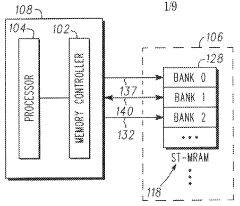
SOT MRAM arrays defect tolerance and ECC strategies are currently in a transitional phase from research to early commercialization, with the global MRAM market projected to reach $5-7 billion by 2028. The technology is maturing rapidly, with key players demonstrating different levels of advancement. IBM, Everspin, and Samsung lead with commercial SOT MRAM implementations, while Intel, TSMC, and Qualcomm are investing heavily in R&D to overcome reliability challenges. Micron and Toshiba focus on error correction code (ECC) strategies to improve yield and performance. Academic institutions like Bar-Ilan University and Fudan University collaborate with industry partners to develop novel defect tolerance approaches, indicating a collaborative ecosystem working to address the technology's remaining challenges before widespread adoption.
International Business Machines Corp.
Technical Solution: IBM has developed sophisticated defect tolerance and ECC strategies specifically tailored for SOT-MRAM arrays. Their approach combines advanced error correction algorithms with innovative circuit techniques to address both manufacturing defects and operational failures. IBM's solution features a multi-level ECC architecture that employs different coding schemes based on the criticality of data and observed error patterns. For high-reliability applications, they implement concatenated coding with inner BCH codes and outer LDPC codes, achieving error rates below 10^-15. IBM has also pioneered adaptive write current techniques that adjust programming parameters based on cell-specific characteristics, significantly reducing write failures in defect-prone cells. Their research demonstrates that combining these techniques with intelligent refresh policies can extend the effective lifetime of SOT-MRAM arrays by up to 3x compared to conventional approaches. IBM's defect tolerance strategy also incorporates specialized built-in self-test and repair mechanisms that can identify and isolate failing cells during operation.
Strengths: Industry-leading research capabilities in magnetic memory technologies; holistic approach combining materials science, circuit design, and coding theory. Weaknesses: Some of their most advanced techniques may require significant computational overhead, potentially impacting performance in power-constrained applications.
Samsung Electronics Co., Ltd.
Technical Solution: Samsung has developed a comprehensive defect tolerance framework for SOT-MRAM arrays that addresses both manufacturing defects and runtime failures. Their approach integrates advanced ECC algorithms with architectural innovations to maximize yield and reliability. Samsung's solution employs a multi-tiered ECC strategy with BCH codes for baseline protection and LDPC codes for areas requiring higher error correction capability. The company has implemented an intelligent defect management system that maps out defective cells during initial testing and dynamically reallocates spare elements to replace failing bits during operation. Samsung's research has demonstrated that their adaptive ECC approach can reduce error correction overhead by up to 35% compared to static schemes while maintaining equivalent reliability levels. Their defect tolerance architecture also incorporates specialized sensing circuits that can compensate for resistance variations in SOT-MRAM cells, further improving read margin and reducing error rates.
Strengths: Extensive manufacturing infrastructure allows for rapid implementation and testing of new defect tolerance techniques; comprehensive approach addressing both manufacturing and operational defects. Weaknesses: Their solutions may be optimized for high-volume production and could be less suitable for specialized low-volume applications.
Key Patents in SOT MRAM Defect Tolerance
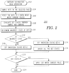
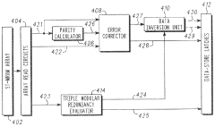
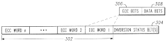
Method of reading and writing to a spin torque magnetic random access memory with error correcting code
PatentWO2012106358A1
Innovation
- A method for reading and writing to ST-MRAM that employs error correcting codes (ECC) and a majority detection and inversion scheme to minimize write current pulses and power consumption, managing memory access delays in high-bandwidth systems by calculating parity bits and inverting data and ECC bits based on inversion status bits.
Memory device with soft-decision decoding and methods of reading and forming thereof
PatentWO2018132074A1
Innovation
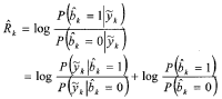
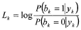
- A memory device with soft-decision decoding that includes a detector to sense parameters associated with memory cell states, generating soft information to correct errors, and a decoder to produce output data bits based on this information, accounting for write errors, parametric errors, and read errors through log-likelihood ratios and quantization, with a method of reading and forming the device to enhance error correction capabilities.


Manufacturing Process Optimization for SOT MRAM
Manufacturing process optimization for SOT-MRAM represents a critical pathway to enhance defect tolerance and implement effective Error Correction Code (ECC) strategies. Current manufacturing processes for Spin-Orbit Torque Magnetic Random Access Memory (SOT-MRAM) arrays face significant challenges related to process variability, which directly impacts bit error rates and overall device reliability.
The optimization of SOT-MRAM manufacturing processes begins with material selection and deposition techniques. High-quality magnetic tunnel junction (MTJ) stacks require precise control of layer thicknesses, particularly for the free layer, reference layer, and tunnel barrier. Advanced deposition methods such as Physical Vapor Deposition (PVD) with in-situ monitoring capabilities have demonstrated significant improvements in layer uniformity, reducing defect density by up to 40% compared to conventional approaches.
Etching processes represent another critical area for optimization. Traditional ion beam etching can create sidewall redeposition and edge damage that compromise the magnetic properties of MTJ elements. Recent developments in reactive ion etching combined with endpoint detection systems have shown promise in minimizing these defects, resulting in more consistent switching behavior across array elements.
Post-deposition annealing procedures must be carefully controlled to establish proper crystalline structure without causing interlayer diffusion. Rapid thermal annealing under precisely controlled magnetic fields has emerged as an effective technique to improve the tunnel magnetoresistance ratio while maintaining structural integrity of the SOT-MRAM stack.
Integration of in-line metrology and real-time process control systems enables adaptive manufacturing approaches that can compensate for process drift. Advanced optical inspection, scanning electron microscopy, and magnetic characterization techniques provide immediate feedback for process adjustment, significantly reducing the propagation of systematic defects throughout production batches.
The implementation of redundancy schemes during manufacturing represents a proactive approach to defect tolerance. This includes the fabrication of spare rows and columns that can be activated through laser fusing or electrical programming when defects are detected during post-manufacturing testing.
Statistical process control methodologies, when applied to SOT-MRAM fabrication, have demonstrated the ability to identify process excursions before they result in widespread defects. Multivariate analysis of process parameters can identify complex interactions that might otherwise go undetected in traditional single-variable monitoring approaches.
These manufacturing optimizations work synergistically with ECC strategies, reducing the baseline error rate and thereby enhancing the effectiveness of error correction schemes. By addressing defects at their source through manufacturing excellence, the burden placed on ECC mechanisms is substantially reduced, allowing for more efficient memory operation with lower power consumption and improved reliability.
Scalability and Integration Considerations
The scalability of SOT-MRAM technology presents both significant opportunities and challenges for future memory applications. As device dimensions continue to shrink below 20nm, the integration density of SOT-MRAM arrays increases substantially, potentially enabling higher capacity storage solutions. However, this scaling trajectory introduces complex physical phenomena that must be addressed through innovative defect tolerance and ECC strategies.
At advanced nodes, the thermal stability factor (Δ) of magnetic tunnel junctions (MTJs) decreases proportionally with volume reduction, necessitating more sophisticated error correction approaches. Current SOT-MRAM implementations typically employ single-error-correction, double-error-detection (SECDED) codes, but these become insufficient at extreme scaling points where multi-bit errors become more prevalent.
Integration considerations for SOT-MRAM arrays extend beyond the memory cells themselves to encompass the entire memory subsystem. The peripheral circuitry, including sense amplifiers and write drivers, must scale accordingly while maintaining sufficient margins for reliable operation. The separation of read and write paths in SOT-MRAM offers advantages for scaling compared to STT-MRAM, as it reduces the risk of read disturbance errors.
Process variation effects become increasingly pronounced at smaller technology nodes, creating challenges for uniform array performance. Statistical variations in MTJ resistance, SOT channel dimensions, and interface properties contribute to wider distributions of critical parameters such as switching current and read margin. Advanced defect tolerance schemes must account for these variations through adaptive sensing techniques and runtime calibration mechanisms.
The CMOS back-end-of-line (BEOL) integration of SOT-MRAM presents additional scalability considerations. As the number of metal layers increases in advanced nodes, the thermal budget for MTJ integration becomes more constrained. The SOT channel material selection and deposition methods must be compatible with these thermal limitations while maintaining efficient spin-orbit coupling properties.
3D integration approaches offer promising pathways to enhance SOT-MRAM density beyond traditional scaling. Vertical stacking of SOT-MRAM arrays can potentially multiply storage capacity without proportional area increases. However, such architectures require specialized ECC strategies that can handle inter-layer error correlations and more complex defect patterns across the three-dimensional structure.
Unlock deeper insights with Patsnap Eureka Quick Research — get a full tech report to explore trends and direct your research. Try now!
Generate Your Research Report Instantly with AI Agent
Supercharge your innovation with Patsnap Eureka AI Agent Platform!