SOT MRAM Intellectual Property And Patent Landscape Overview
AUG 28, 20259 MIN READ
Generate Your Research Report Instantly with AI Agent
Patsnap Eureka helps you evaluate technical feasibility & market potential.
SOT MRAM Technology Background and Objectives
Spin-Orbit Torque Magnetoresistive Random Access Memory (SOT MRAM) represents a significant evolution in non-volatile memory technology, emerging from decades of research in spintronics and magnetic materials. The technology builds upon the foundation established by conventional MRAM and Spin-Transfer Torque MRAM (STT-MRAM), addressing critical limitations in write energy efficiency, endurance, and scalability that have constrained previous generations of magnetic memory.
The development of SOT MRAM can be traced back to fundamental discoveries in spin-orbit coupling phenomena in the early 2000s, followed by experimental demonstrations of spin-orbit torque switching in 2011-2012. This breakthrough enabled a paradigm shift in how magnetic states can be manipulated in memory devices, separating the read and write paths to overcome the reliability-speed tradeoff inherent in STT-MRAM.
The global research landscape has witnessed accelerating interest in SOT MRAM technology since 2015, with patent filings showing exponential growth between 2016-2021. This surge reflects recognition of SOT MRAM's potential to deliver a universal memory solution combining the speed of SRAM, the density of DRAM, and the non-volatility of flash memory, while consuming significantly less power than existing technologies.
The primary technical objective driving SOT MRAM development is to create a commercially viable memory technology that can operate at sub-nanosecond switching speeds while maintaining reliability at advanced technology nodes below 10nm. This would position SOT MRAM as a critical enabler for next-generation computing architectures, particularly for applications requiring ultra-low power consumption and high endurance.
Secondary objectives include reducing the critical switching current density to enable compatibility with standard CMOS processes, enhancing thermal stability for enterprise and automotive applications requiring operation at elevated temperatures, and developing material stacks compatible with back-end-of-line integration for embedded memory applications.
The technology trajectory suggests SOT MRAM is approaching an inflection point, transitioning from fundamental research to commercial development. Major semiconductor manufacturers and research institutions have established significant intellectual property portfolios, indicating preparation for market entry within the next 3-5 years. This transition is supported by recent demonstrations of functional SOT MRAM devices at 22nm node with performance characteristics that outpace competing non-volatile memory technologies.
As computing paradigms shift toward edge AI, IoT, and neuromorphic architectures, SOT MRAM's unique combination of speed, endurance, and energy efficiency positions it as a potentially transformative technology for the semiconductor industry, capable of addressing the memory wall challenge that has increasingly constrained computing performance.
Market Demand Analysis for SOT MRAM Solutions
The SOT MRAM (Spin-Orbit Torque Magnetoresistive Random Access Memory) market is experiencing significant growth driven by increasing demand for non-volatile memory solutions with enhanced performance characteristics. Current market analysis indicates that the global MRAM market, which includes SOT MRAM, is projected to grow at a compound annual growth rate of over 30% through 2028, with the total addressable market expected to reach several billion dollars by the end of the decade.
The primary market demand for SOT MRAM stems from data centers and enterprise storage systems, where there is a critical need for memory solutions that combine the speed of SRAM with the non-volatility of flash memory. These sectors value SOT MRAM's unique combination of unlimited endurance, fast switching speeds, and non-volatility, which addresses the growing challenges of power consumption and data persistence in high-performance computing environments.
Automotive and industrial IoT applications represent another significant market segment for SOT MRAM solutions. The automotive industry, particularly with the rise of autonomous vehicles and advanced driver-assistance systems, requires memory technologies that can operate reliably under extreme temperature conditions while maintaining data integrity. SOT MRAM's radiation hardness and temperature stability make it particularly suitable for these demanding environments.
Consumer electronics manufacturers are also showing increased interest in SOT MRAM technology for next-generation smartphones, wearables, and other portable devices. The technology's low power consumption characteristics align perfectly with the industry's push toward more energy-efficient devices with longer battery life. Market research indicates that consumer electronics could become the largest volume market for SOT MRAM within the next five years.
Edge computing applications represent an emerging market opportunity for SOT MRAM solutions. As computational tasks increasingly move to the network edge, the demand for memory technologies that can support rapid, energy-efficient data processing continues to grow. SOT MRAM's combination of speed and non-volatility positions it as an ideal candidate for these applications.
From a regional perspective, North America currently leads in SOT MRAM adoption, primarily due to the concentration of data center operations and semiconductor research facilities. However, the Asia-Pacific region is expected to witness the fastest growth rate, driven by the expanding electronics manufacturing sector and increasing investments in advanced memory technologies by countries like China, South Korea, and Japan.
Market analysis also reveals a growing trend toward the integration of SOT MRAM in embedded systems, particularly in applications requiring secure, persistent storage of sensitive data. The financial services sector, healthcare industry, and military applications are increasingly exploring SOT MRAM solutions for secure data storage needs, further expanding the potential market reach of this technology.
Global SOT MRAM Development Status and Challenges
Spin-Orbit Torque Magnetoresistive Random Access Memory (SOT MRAM) technology has emerged as a promising candidate for next-generation non-volatile memory solutions. Currently, the global development of SOT MRAM faces both significant progress and substantial challenges across different regions and research institutions.
In the United States, major semiconductor companies including Intel, IBM, and Qualcomm have established strong research programs focused on SOT MRAM development. These efforts are complemented by academic research at institutions such as MIT, Stanford University, and the University of California. The U.S. leads in fundamental research publications and holds a significant portion of SOT MRAM-related patents.
European development is centered around research consortiums like IMEC in Belgium and CEA-Leti in France, which have demonstrated promising SOT MRAM prototypes. These institutions collaborate closely with companies such as STMicroelectronics and Infineon Technologies to bridge the gap between academic research and commercial applications.
In Asia, particularly in South Korea and Japan, companies like Samsung, SK Hynix, and Toshiba are making substantial investments in SOT MRAM technology. China has also accelerated its efforts through initiatives at research institutions including the Chinese Academy of Sciences and Tsinghua University.
Despite this global progress, SOT MRAM faces several critical technical challenges. The primary obstacle remains the efficiency of spin-orbit torque generation, which directly impacts switching speed and energy consumption. Current devices require relatively high current densities for reliable switching, limiting their practical application in low-power environments.
Material integration presents another significant challenge. The complex stack structure of SOT MRAM devices, typically involving magnetic multilayers, heavy metal layers, and tunnel barriers, creates difficulties in manufacturing compatibility with standard CMOS processes. Maintaining structural and functional integrity during back-end-of-line processing remains problematic.
Scaling issues also persist as a major hurdle. As device dimensions shrink below 20nm, maintaining thermal stability while ensuring reliable switching becomes increasingly difficult. This fundamental physics challenge requires innovative materials engineering and device architecture solutions.
Reliability and endurance represent additional concerns. While SOT MRAM theoretically offers unlimited write endurance compared to other non-volatile memories, practical implementations still face challenges related to material degradation and interface quality over extended cycling.
The commercialization pathway faces economic challenges as well. The cost-performance balance remains unfavorable compared to established memory technologies, requiring further optimization of manufacturing processes and materials to achieve competitive pricing for mass-market adoption.
Current SOT MRAM Technical Solutions
01 SOT-MRAM device structures and fabrication methods
Various patents describe innovative device structures and fabrication methods for SOT-MRAM technology. These include specific layer configurations, material compositions, and manufacturing techniques designed to enhance performance and reliability. The innovations focus on optimizing the magnetic tunnel junction (MTJ) structure, improving spin-orbit coupling effects, and developing scalable fabrication processes for commercial production.- SOT MRAM device structures and fabrication methods: Various patents describe specific device structures and fabrication methods for SOT MRAM technology. These include innovations in the design of magnetic tunnel junctions (MTJs), integration of SOT elements with CMOS technology, and novel manufacturing processes to enhance device performance and reliability. These structural innovations aim to improve switching efficiency, reduce power consumption, and increase memory density in SOT MRAM devices.
- Spin-orbit torque generation and control mechanisms: This category focuses on methods and materials for generating and controlling spin-orbit torques in MRAM devices. Innovations include specialized materials with high spin-orbit coupling, novel electrode configurations, and techniques for manipulating spin current direction and magnitude. These advancements enable more efficient magnetization switching, lower critical currents, and improved operational stability in SOT MRAM devices.
- SOT MRAM cell architecture and array organization: Patents in this category address the organization and architecture of SOT MRAM cells within memory arrays. Innovations include cell layout designs, bit line and word line configurations, and addressing schemes that optimize memory density and performance. These architectural approaches aim to improve read/write speeds, reduce cross-talk between adjacent cells, and enhance overall memory array efficiency.
- Integration with peripheral circuits and systems: This category covers innovations related to the integration of SOT MRAM with peripheral circuits and larger computing systems. Patents describe sense amplifiers, write drivers, control logic, and interface circuits specifically designed for SOT MRAM operation. These developments enable seamless integration with existing semiconductor technologies and optimize the performance of SOT MRAM in various computing applications.
- Advanced materials and multilayer structures for SOT MRAM: Patents in this category focus on novel materials and multilayer structures to enhance SOT MRAM performance. Innovations include specialized heavy metal layers, engineered interfaces, and composite magnetic materials that improve spin-orbit coupling efficiency and magnetic switching characteristics. These material advancements aim to reduce switching energy, improve thermal stability, and enhance the endurance of SOT MRAM devices.
02 Write and read operation mechanisms for SOT-MRAM
These patents cover innovations in the write and read operation mechanisms of SOT-MRAM devices. They describe methods to improve writing efficiency using spin-orbit torque, techniques for reducing write current requirements, and approaches for enhancing read reliability. The technologies aim to address challenges in switching speed, energy consumption, and signal-to-noise ratio during memory operations.Expand Specific Solutions03 Integration of SOT-MRAM with semiconductor technologies
This category focuses on the integration of SOT-MRAM with existing semiconductor technologies and architectures. The patents describe methods for incorporating SOT-MRAM into CMOS processes, techniques for creating hybrid memory systems, and approaches for designing SOT-MRAM-based computing architectures. These innovations aim to leverage the non-volatility and energy efficiency of SOT-MRAM in various computing applications.Expand Specific Solutions04 Material innovations for SOT-MRAM performance enhancement
These patents cover novel materials and material combinations designed to enhance SOT-MRAM performance. They include innovations in magnetic materials, heavy metal layers for improved spin-orbit coupling, and interface engineering techniques. The materials research aims to improve thermal stability, reduce critical switching current, enhance magnetoresistance ratio, and extend device endurance.Expand Specific Solutions05 Circuit designs and architectures for SOT-MRAM implementation
This category encompasses circuit designs and memory architectures specifically optimized for SOT-MRAM implementation. The patents describe sense amplifier designs, addressing schemes, and peripheral circuitry innovations that address the unique characteristics of SOT-MRAM. These circuit-level innovations aim to maximize the benefits of SOT-MRAM technology while mitigating potential challenges in large-scale memory arrays.Expand Specific Solutions
Key Industry Players in SOT MRAM Development
The SOT MRAM intellectual property landscape is currently in a growth phase, with the market expected to reach significant expansion as this emerging non-volatile memory technology matures. Major semiconductor players like IBM, TSMC, and Samsung Electronics are leading patent development, with IBM demonstrating particular dominance in the intellectual property space. Research institutions including IMEC, Katholieke Universiteit Leuven, and various Asian universities are contributing fundamental innovations. The competitive landscape shows a mix of established semiconductor manufacturers (GlobalFoundries, Applied Materials), specialized memory companies (Everspin Technologies, KIOXIA), and research-focused entities collaborating to overcome technical challenges in scalability and manufacturing. The technology is approaching commercial maturity with increasing patent activity focused on integration with conventional CMOS processes.
International Business Machines Corp.
Technical Solution: IBM has pioneered significant advancements in SOT MRAM technology, focusing on high-performance computing applications. Their technical approach involves three-terminal SOT MRAM designs that separate the read and write paths, enabling faster switching speeds and lower energy consumption. IBM's SOT MRAM architecture utilizes heavy metal layers (typically tungsten or platinum) adjacent to magnetic tunnel junctions to generate spin currents that efficiently switch the free layer magnetization. The company has developed specialized fabrication techniques that maintain thermal stability while reducing the critical switching current density to below 10^7 A/cm². IBM has also integrated SOT MRAM with CMOS technology at advanced nodes (7nm and below), demonstrating functional memory arrays with sub-nanosecond write speeds and endurance exceeding 10^12 cycles.
Strengths: Superior switching speed (sub-ns) compared to STT-MRAM; excellent endurance; CMOS compatibility at advanced nodes; reduced read disturbance. Weaknesses: Higher fabrication complexity requiring additional materials and process steps; larger cell size due to three-terminal design; challenges in scaling the technology for high-density applications.
Taiwan Semiconductor Manufacturing Co., Ltd.
Technical Solution: TSMC has developed a comprehensive SOT MRAM manufacturing platform that integrates with their advanced logic processes. Their technical solution focuses on material engineering and process optimization to enable SOT MRAM as embedded memory for logic applications. TSMC's approach utilizes specialized heavy metal/ferromagnet interfaces with enhanced spin-orbit coupling to achieve efficient spin current generation. They have pioneered a unique dual damascene process for SOT MRAM integration that maintains CMOS compatibility while minimizing thermal budget issues. TSMC has demonstrated functional 28nm SOT MRAM test chips with write currents below 200μA and switching times under 5ns. Their technology roadmap includes scaling to more advanced nodes with reduced critical dimensions of the SOT channel to further improve energy efficiency and density.
Strengths: Mature manufacturing infrastructure; excellent process integration capabilities; strong ecosystem partnerships enabling rapid commercialization; demonstrated reliability in production environments. Weaknesses: Relatively higher manufacturing costs compared to conventional embedded memories; thermal stability challenges at advanced nodes; write current variability across wafers.
Critical Patents and Technical Literature Analysis
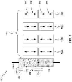
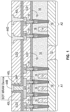
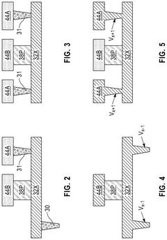
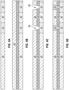
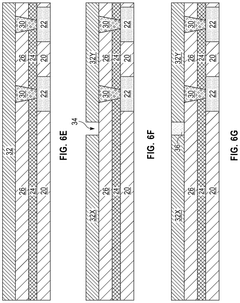
Spin-orbit torque and spin-transfer torque magnetoresistive random-access memory stack
PatentActiveUS12016251B2
Innovation
- The integration of a spin-transfer torque (STT) MRAM stack with a spin-orbit torque (SOT) MRAM stack in series, utilizing a heavy metal rail to flip the SOT free-layer magnetic orientation in response to horizontal signals, enabling four distinct resistance states (00, 01, 10, 11) for efficient weight storage, thereby reducing power consumption and hardware requirements.
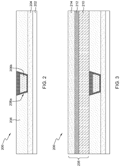
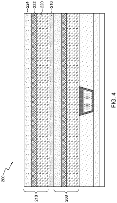
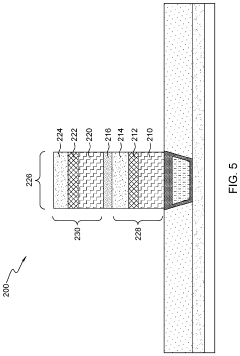
Spin-orbit torque memory devices
PatentPendingUS20240324468A1
Innovation
- Integrating a SOT layer and an interconnect layer at the same metal level using a topological conductor as both the interconnect and SOT layer, eliminating the need for SOT via layers and simplifying patterning, thereby allowing insertion at a lower metal level.
IP Landscape and Patent Strategy Considerations
The SOT MRAM intellectual property landscape has evolved significantly over the past decade, with a notable acceleration in patent filings since 2015. Major semiconductor companies including Samsung, Intel, IBM, and TSMC have established substantial patent portfolios, creating a complex competitive environment. These portfolios primarily focus on materials engineering, device structures, and manufacturing processes, reflecting the multidisciplinary nature of SOT MRAM technology.
Patent concentration analysis reveals geographical clustering in the United States, South Korea, Japan, and increasingly China, with specialized research institutions and universities contributing significantly to fundamental innovations. The patent landscape shows a transition from broad conceptual patents to more specific implementation-focused intellectual property, indicating technology maturation.
Freedom-to-operate considerations are particularly challenging in the SOT MRAM space due to overlapping claims and the fundamental nature of early patents. Companies entering this field must conduct thorough patent clearance searches and consider strategic licensing agreements with key patent holders to mitigate infringement risks.
Cross-licensing opportunities represent a viable strategy for companies with complementary IP portfolios. For instance, firms with strong materials patents might benefit from partnerships with companies holding manufacturing process patents, creating mutually beneficial arrangements that accelerate commercialization timelines.
Defensive patenting strategies have become increasingly important as the technology approaches wider commercial adoption. Companies are filing patents not only on core technologies but also on adjacent innovations and potential workarounds to strengthen their competitive positions and provide negotiating leverage.
Patent quality varies significantly across the landscape, with some filings representing fundamental breakthroughs while others constitute incremental improvements or defensive filings. Evaluating the strength and enforceability of patents requires careful analysis of claim scope, prior art considerations, and jurisdictional coverage.
For new entrants, strategic approaches include focusing on underexplored niches within the SOT MRAM ecosystem, developing patent portfolios around specific applications, and considering acquisitions of smaller companies with valuable IP assets. Additionally, participating in industry standards development can provide strategic advantages in shaping the technology's future direction while securing essential patent positions.
Standardization and Industry Collaboration Opportunities
The standardization of SOT MRAM technology represents a critical pathway for industry-wide adoption and commercialization. Currently, several industry consortia, including JEDEC and IEEE, are actively working on establishing technical standards for MRAM technologies, with specific focus emerging on SOT MRAM as its commercial viability increases. These standardization efforts primarily address interface protocols, performance benchmarks, reliability metrics, and testing methodologies.
Collaborative research initiatives between academic institutions and industry leaders have accelerated SOT MRAM development significantly. Notable partnerships include collaborations between Samsung and IBM, TSMC and research universities, and Intel's investment in joint development programs. These collaborations have yielded substantial advancements in material science and device architecture, particularly in addressing the challenges of thermal stability and switching efficiency.
Open innovation platforms are emerging as valuable vehicles for SOT MRAM advancement. Organizations like IMEC and GLOBALFOUNDRIES have established shared research facilities where multiple stakeholders can contribute to solving common technical challenges while maintaining their proprietary innovations. This collaborative approach has proven effective in addressing fundamental material science issues that would be prohibitively expensive for individual companies to solve independently.
Patent pools and cross-licensing agreements present significant opportunities for accelerating SOT MRAM commercialization. The current fragmented patent landscape creates barriers to market entry and increases development costs. Industry leaders could benefit from establishing structured licensing frameworks that enable broader access to fundamental SOT MRAM technologies while preserving competitive advantages in specific applications or implementation methods.
Standardized testing and qualification protocols represent another critical area for industry collaboration. The development of uniform reliability assessment methodologies would significantly reduce qualification time for new SOT MRAM products and increase customer confidence. Current efforts by semiconductor equipment manufacturers to establish standardized characterization techniques will likely accelerate adoption across multiple market segments.
International cooperation frameworks, particularly between research institutions in the United States, Europe, and Asia, offer promising avenues for addressing fundamental scientific challenges in SOT MRAM development. These collaborations could potentially overcome geopolitical tensions surrounding semiconductor technology by focusing on pre-competitive research areas that benefit the entire ecosystem while allowing for regional specialization in specific applications or manufacturing techniques.
Unlock deeper insights with Patsnap Eureka Quick Research — get a full tech report to explore trends and direct your research. Try now!
Generate Your Research Report Instantly with AI Agent
Supercharge your innovation with Patsnap Eureka AI Agent Platform!