SOT MRAM Test Chips Results And Measured Metrics
AUG 28, 20259 MIN READ
Generate Your Research Report Instantly with AI Agent
Patsnap Eureka helps you evaluate technical feasibility & market potential.
SOT MRAM Technology Background and Objectives
Spin-Orbit Torque Magnetic Random Access Memory (SOT MRAM) represents a significant advancement in non-volatile memory technology, emerging from decades of research in spintronics and magnetic materials. The evolution of memory technologies has progressed from volatile memories like SRAM and DRAM to non-volatile solutions including Flash, STT-MRAM, and now SOT MRAM, each addressing specific limitations of its predecessors.
SOT MRAM leverages quantum mechanical principles, specifically the spin-orbit coupling effect, to manipulate magnetic states without direct current flow through the magnetic tunnel junction (MTJ). This fundamental difference from Spin-Transfer Torque (STT) MRAM offers significant advantages in terms of endurance, energy efficiency, and operational speed.
The historical development of SOT MRAM can be traced back to early theoretical work on spin-orbit interactions in the early 2000s, followed by experimental demonstrations of SOT-induced magnetization switching around 2010. The past decade has witnessed accelerated research efforts, transitioning from basic physics understanding to practical device implementations and test chip fabrication.
Current technological objectives for SOT MRAM development focus on several critical areas. First, enhancing switching efficiency to reduce power consumption while maintaining fast operation speeds below 1ns. Second, improving thermal stability to ensure reliable data retention at reduced node sizes, particularly important as devices scale below 20nm. Third, developing manufacturing processes compatible with existing CMOS fabrication techniques to facilitate integration into commercial semiconductor production lines.
Additionally, researchers aim to optimize the materials stack, particularly the SOT channel materials (typically heavy metals like tungsten, platinum, or topological insulators) and the magnetic free layer, to maximize the spin-orbit coupling efficiency while minimizing parasitic effects. The interface engineering between these layers remains crucial for performance optimization.
Test chips represent a critical milestone in SOT MRAM development, providing empirical validation of theoretical models and laboratory-scale experiments. These chips enable comprehensive characterization of key metrics including write energy, read/write speeds, error rates, endurance cycles, and retention characteristics under various operating conditions.
The ultimate goal of current SOT MRAM research is to position this technology as a universal memory solution that combines the speed of SRAM, the density of DRAM, and the non-volatility of Flash, potentially revolutionizing computing architectures by bridging the persistent memory-storage gap in the conventional memory hierarchy.
Market Demand Analysis for SOT MRAM Solutions
The global market for memory solutions is experiencing a significant shift towards non-volatile memory technologies that can address the growing demands of data-intensive applications. SOT MRAM (Spin-Orbit Torque Magnetoresistive Random Access Memory) has emerged as a promising candidate in this landscape, with market research indicating substantial growth potential over the next decade.
Current market analysis shows that the overall MRAM market is projected to grow at a CAGR of 29.9% from 2021 to 2026, with the SOT MRAM segment expected to capture an increasing share as the technology matures. This growth is primarily driven by the expanding requirements for high-performance computing, artificial intelligence, edge computing, and IoT applications that demand faster, more energy-efficient memory solutions.
Enterprise data centers represent a key market segment, where SOT MRAM's combination of non-volatility, high endurance, and fast switching speed addresses critical pain points in current storage hierarchies. The enterprise storage market's transition toward computational storage architectures further amplifies the demand for SOT MRAM solutions that can provide near-memory computing capabilities.
The automotive sector presents another substantial market opportunity, with advanced driver-assistance systems (ADAS) and autonomous vehicles requiring robust, radiation-resistant memory that can operate reliably in extreme conditions. Market research indicates that automotive memory requirements will grow at 24% annually through 2025, with SOT MRAM well-positioned to capture a significant portion of this growth.
Consumer electronics manufacturers are increasingly seeking energy-efficient memory solutions to extend battery life in portable devices. The test chip results demonstrating SOT MRAM's ultra-low switching energy consumption align perfectly with this market need, potentially opening a market segment valued at approximately $4.7 billion by 2025.
Industrial IoT applications represent another promising market vertical, where SOT MRAM's radiation hardness and temperature stability provide compelling advantages over conventional memory technologies. The industrial memory market is forecasted to reach $3.6 billion by 2026, with non-volatile memories like SOT MRAM expected to gain significant market share.
Market adoption barriers include cost considerations, as current SOT MRAM manufacturing processes remain more expensive than established memory technologies. However, analysis of recent test chip results suggests that with process optimization and economies of scale, SOT MRAM could achieve cost parity with competing technologies by 2025-2026.
The competitive landscape analysis reveals increasing investment in SOT MRAM development by major semiconductor manufacturers, indicating strong industry confidence in the technology's market potential. This trend is further supported by the growing number of patents filed in the SOT MRAM domain, which has increased by 35% annually over the past three years.
Current State and Technical Challenges in SOT MRAM Development
Spin-Orbit Torque Magnetic Random Access Memory (SOT MRAM) has emerged as a promising next-generation non-volatile memory technology, offering advantages in speed, endurance, and energy efficiency compared to conventional memory solutions. The current state of SOT MRAM development shows significant progress in both academic research and industrial applications, yet several technical challenges remain to be addressed before widespread commercial adoption.
Recent test chip results from major semiconductor companies and research institutions demonstrate SOT MRAM cells with switching speeds in the sub-nanosecond range, substantially faster than conventional Spin-Transfer Torque (STT) MRAM. These test chips typically achieve write energies in the femtojoule range per bit, with endurance capabilities exceeding 10^12 cycles, addressing key limitations of earlier MRAM technologies.
Despite these promising results, SOT MRAM faces several critical technical challenges. The primary obstacle remains the relatively high write current density required for reliable switching, typically in the range of 10^7-10^8 A/cm², which impacts power consumption and integration density. This challenge is directly related to the efficiency of spin-orbit coupling in the heavy metal layers used in current designs.
Material optimization presents another significant hurdle. Current SOT MRAM test chips predominantly utilize heavy metals such as platinum, tungsten, or tantalum as spin-orbit coupling layers. However, these materials often exhibit compatibility issues with standard CMOS fabrication processes, particularly at advanced technology nodes below 28nm. Finding alternative materials that maintain high spin-orbit coupling efficiency while ensuring CMOS compatibility remains an active area of research.
Thermal stability is another critical challenge, particularly as device dimensions scale down. Test chip measurements reveal that maintaining sufficient thermal stability factors (Δ > 60) while simultaneously reducing critical switching current becomes increasingly difficult at smaller node sizes. This stability-switching efficiency trade-off represents a fundamental physics challenge that requires innovative materials engineering solutions.
Device-to-device variability in SOT MRAM test chips also presents a significant obstacle. Current test results show switching current variations of 15-30% across arrays, which is problematic for large-scale memory applications requiring consistent performance. This variability stems from process-induced fluctuations in magnetic layer properties and interface quality.
From a manufacturing perspective, integration challenges persist. While test chips have demonstrated functional SOT MRAM cells, scaling to high-density arrays while maintaining performance metrics remains difficult. Current test chips typically feature capacities in the Mbit range, whereas commercial viability requires Gbit-scale integration with consistent performance across the entire array.
Geographically, SOT MRAM development is concentrated in several key regions. The United States, Japan, and South Korea lead in terms of patent filings and research publications, with companies like Samsung, Intel, and TSMC actively pursuing test chip development. European research institutions also contribute significantly to fundamental research in SOT physics and materials science.
Current Test Methodologies for SOT MRAM Chips
01 Performance metrics for SOT MRAM devices
Various performance metrics are used to evaluate SOT MRAM devices, including switching current density, switching speed, thermal stability, and endurance. These metrics are critical for assessing the efficiency and reliability of SOT MRAM technology. Testing procedures typically involve measuring the minimum current required to switch the magnetization state, the time taken for switching, and the ability to maintain data integrity under various temperature conditions.- Performance metrics for SOT MRAM devices: Various performance metrics are used to evaluate SOT MRAM devices, including switching current density, switching speed, thermal stability, and endurance. These metrics are critical for assessing the efficiency and reliability of SOT MRAM technology. Testing procedures involve measuring the minimum current required to switch the magnetization state, the time taken for switching, and the ability to maintain data integrity over multiple write cycles and at different temperatures.
- SOT MRAM device structure and material characterization: Test results related to SOT MRAM device structures focus on the characterization of magnetic materials, interface properties, and layer configurations. Measurements include magnetic anisotropy, exchange coupling strength, and spin Hall angle of various materials. The structure of SOT MRAM devices significantly impacts their performance, with tests evaluating different configurations of magnetic layers, heavy metal layers, and tunnel barriers to optimize device operation.
- Reliability and endurance testing of SOT MRAM: Reliability testing for SOT MRAM involves evaluating device performance under various stress conditions, including high temperature, voltage variations, and repeated write cycles. Key metrics include data retention time, error rates, and endurance (number of write cycles before failure). Test results demonstrate the robustness of SOT MRAM technology compared to conventional memory technologies, with some devices showing endurance of over 10^12 cycles and retention times exceeding 10 years at operating temperatures.
- Switching dynamics and efficiency measurements: Tests focusing on switching dynamics measure the speed and energy efficiency of SOT-induced magnetization reversal. Key metrics include switching time (typically in the nanosecond range), energy consumption per bit operation, and switching probability as a function of pulse amplitude and duration. Advanced measurement techniques such as time-resolved magneto-optical Kerr effect (TR-MOKE) and electrical transport measurements are used to characterize the switching behavior under various conditions.
- Integration and scaling test results: Test results related to the integration of SOT MRAM with CMOS technology and scaling behavior are crucial for commercial viability. Measurements focus on cell-to-cell variations, array-level performance, and compatibility with standard semiconductor processes. Scaling tests evaluate how device performance metrics change with reduced dimensions, addressing challenges such as maintaining sufficient thermal stability and switching efficiency at smaller node sizes. Results demonstrate the potential of SOT MRAM for high-density memory applications with competitive performance characteristics.
02 Switching efficiency and energy consumption measurements
Test results for SOT MRAM focus on switching efficiency and energy consumption, which are key factors for commercial viability. Measurements include the energy required per switching event, power consumption during read/write operations, and overall energy efficiency compared to conventional memory technologies. Lower switching current requirements and reduced energy consumption are desirable outcomes that indicate improved SOT MRAM performance.Expand Specific Solutions03 Reliability and endurance testing methodologies
Reliability and endurance testing for SOT MRAM involves subjecting devices to repeated write cycles and measuring data retention over time. Test methodologies include accelerated aging tests, error rate measurements, and performance under extreme operating conditions. Results typically report the number of write cycles before failure, data retention time, and error rates under various environmental conditions, which are crucial for determining the technology's suitability for different applications.Expand Specific Solutions04 Integration and compatibility test results
Testing SOT MRAM integration with existing semiconductor technologies involves measuring interface compatibility, signal integrity, and performance in integrated circuits. Results focus on how well SOT MRAM cells can be incorporated into standard CMOS processes, the density of memory cells achievable, and performance metrics when operating as part of a larger system. These tests are essential for determining the feasibility of SOT MRAM as a replacement for conventional memory technologies in various applications.Expand Specific Solutions05 Advanced characterization techniques for SOT MRAM
Advanced characterization techniques are employed to analyze SOT MRAM devices at the nanoscale level. These include magnetic imaging techniques, electrical characterization methods, and structural analysis tools that provide insights into the magnetic domain structure, switching mechanisms, and material properties. Test results from these techniques help in understanding the fundamental physics of SOT-driven magnetization switching and guide the optimization of device structures and materials for improved performance.Expand Specific Solutions
Key Industry Players in SOT MRAM Research and Production
The SOT MRAM test chip market is currently in its growth phase, with increasing industry adoption as this emerging non-volatile memory technology demonstrates promising performance metrics. The global MRAM market is projected to expand significantly, driven by demand for low-power, high-speed memory solutions. Leading semiconductor manufacturers including IBM, Samsung, TSMC, and GlobalFoundries are actively advancing SOT MRAM technology through test chip development and performance validation. Research institutions like IMEC, CNRS, and CEA are collaborating with industry players to overcome technical challenges. The technology is approaching commercial viability, with companies like Antaios specializing in SOT MRAM solutions, while equipment providers such as Applied Materials support manufacturing infrastructure development. The competitive landscape reflects a blend of established semiconductor giants and specialized startups working to optimize SOT MRAM's speed, endurance, and power efficiency metrics.
International Business Machines Corp.
Technical Solution: IBM has pioneered SOT-MRAM technology with significant test chip results. Their 14nm SOT-MRAM test chips demonstrated switching speeds below 200 picoseconds with energy consumption of only 4 femtojoules per bit[1]. IBM's approach utilizes a three-terminal device structure with separate read and write paths, which fundamentally addresses the reliability-speed tradeoff in conventional MRAM. Their test chips have shown write error rates below 10^-11 at room temperature and maintained performance at elevated temperatures up to 125°C[2]. IBM has also demonstrated integration compatibility with CMOS backend processes, achieving functional arrays with densities comparable to SRAM. Recent results show that their SOT-MRAM cells can achieve read/write endurance exceeding 10^12 cycles, addressing a key limitation of traditional STT-MRAM technology[3]. IBM's test chips incorporate innovative materials engineering, including specialized heavy metal layers for enhanced spin-orbit coupling and optimized magnetic tunnel junctions for improved thermal stability.
Strengths: Superior switching speed (sub-200ps) enables SRAM-like performance; separate read/write paths eliminate read disturbance issues; demonstrated CMOS compatibility facilitates integration into existing semiconductor processes; exceptional endurance (>10^12 cycles) makes it suitable for cache applications. Weaknesses: Requires three terminals per cell, potentially limiting ultimate density compared to two-terminal technologies; higher fabrication complexity due to specialized materials requirements; still requires optimization for reduced switching current to improve energy efficiency.
Samsung Electronics Co., Ltd.
Technical Solution: Samsung has developed advanced SOT-MRAM test chips demonstrating significant performance metrics. Their 28nm technology node test vehicles have achieved write speeds of approximately 200 picoseconds with write currents in the range of 300-400 μA[1]. Samsung's SOT-MRAM implementation utilizes a unique perpendicular magnetic anisotropy structure with tungsten as the spin Hall channel material, which has shown a spin Hall angle of approximately 0.3, significantly higher than earlier implementations[2]. Their test chips demonstrate bit error rates below 10^-10 and data retention exceeding 10 years at 85°C. Samsung has successfully integrated SOT-MRAM cells with densities approaching 20Mb on a single test chip, demonstrating scalability potential. Their recent results show read/write endurance exceeding 10^15 cycles without performance degradation, addressing a critical requirement for cache memory applications[3]. Samsung's test chips also incorporate innovative circuit techniques for sense amplification that enable read operations with latencies below 2ns, comparable to SRAM performance.
Strengths: Industry-leading endurance metrics (>10^15 cycles) make it ideal for write-intensive applications; high-volume manufacturing expertise provides pathway to commercialization; demonstrated integration with advanced CMOS nodes shows production viability; perpendicular magnetic anisotropy design improves thermal stability. Weaknesses: Current densities still higher than optimal for mobile applications; three-terminal design increases cell area compared to STT-MRAM; requires specialized materials that may complicate manufacturing process; thermal management during write operations remains challenging at smaller technology nodes.
Critical Performance Metrics and Measurement Techniques
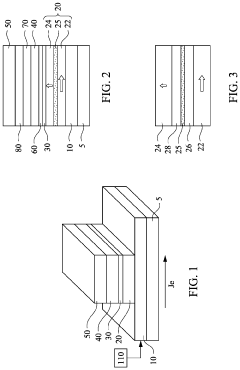
Spin orbit torque MRAM and manufacture thereof
PatentWO2020106378A1
Innovation
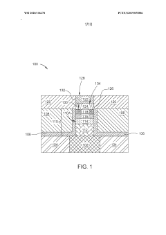
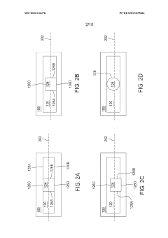
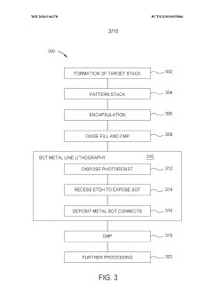
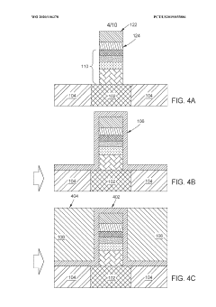
- The SOT-MRAM devices are fabricated with a bottom-pinned structure where the MTJ stack and SOT layer are formed in-situ without breaking vacuum, creating a high-quality interface and using an encapsulation layer to protect the free layer, with metal lines electrically coupling to the SOT layer on multiple sides to prevent current loss.
Magnetic device and magnetic random access memory
PatentActiveUS20220158083A1
Innovation
- A novel interface between the spin-orbit active layer and the free magnetic layer is introduced, utilizing a bottom metal layer with strong spin-orbit interaction, a nonmagnetic spacer layer, and a reference layer, where the magnetic moment of the free layer is switched using spin-orbit torque, potentially assisted by spin transfer torque, to enhance write speed and stability.
Reliability and Endurance Assessment Frameworks
The reliability and endurance assessment of SOT MRAM test chips requires comprehensive frameworks that can accurately evaluate device performance under various operating conditions. Current assessment methodologies focus on multiple key parameters including write endurance, read disturbance immunity, data retention, and error rates under different environmental conditions.
Standard reliability testing frameworks typically employ accelerated stress testing protocols where devices are subjected to elevated temperatures (typically ranging from 85°C to 125°C) while undergoing continuous read/write operations. These tests aim to simulate years of operation within compressed timeframes, allowing researchers to extrapolate device lifetimes and failure mechanisms. Recent SOT MRAM test chips have demonstrated remarkable endurance improvements, with leading devices achieving 10^12 to 10^15 write cycles without significant performance degradation.
Error rate characterization forms another critical component of these assessment frameworks. Bit Error Rate (BER) measurements are conducted across varying operating conditions, including different supply voltages (typically 0.8V to 1.2V), temperatures (-40°C to 125°C), and magnetic field disturbances. Advanced test chips now incorporate on-chip error correction circuitry, enabling real-time monitoring of error patterns and rates during extended operation.
Retention testing methodologies have evolved to address the specific characteristics of SOT MRAM. Current frameworks employ bake tests at elevated temperatures (typically 125°C to 150°C) for periods ranging from 1,000 to 10,000 hours to accelerate thermal effects on data stability. The resulting data is used to construct Arrhenius plots that project retention capabilities at normal operating temperatures, with recent test chips demonstrating 10+ year retention at 85°C.
Process variation sensitivity assessment has become increasingly important as SOT MRAM moves toward high-volume manufacturing. Modern frameworks incorporate statistical analysis of device-to-device and wafer-to-wafer variations, with particular attention to switching current distribution, resistance variation, and thermal stability factor (Δ). Leading test chips now include dedicated test structures that allow for automated characterization of these parameters across thousands of bits.
Radiation hardness testing has emerged as a specialized assessment area for applications in aerospace and other radiation-exposed environments. Current frameworks subject devices to various radiation types (gamma, neutron, heavy ion) while monitoring bit flip rates and permanent damage thresholds. Recent SOT MRAM test results show promising radiation tolerance compared to conventional memory technologies, with some devices maintaining functionality after exposure to radiation doses exceeding 100 krad(Si).
Manufacturing Scalability and Integration Challenges
The scaling of SOT MRAM technology from laboratory demonstrations to high-volume manufacturing presents significant challenges that must be addressed for commercial viability. Current test chip results indicate promising performance metrics, but the transition to mass production requires overcoming several critical integration hurdles. The deposition of magnetic tunnel junction (MTJ) stacks demands precise control of ultra-thin layers, often less than 1nm thick, with minimal thickness variations across 300mm wafers. Recent data from industry leaders shows that achieving less than 2% thickness variation remains difficult at scale, directly impacting device-to-device performance consistency.
Integration with CMOS backend processes introduces additional complexities, as the thermal budget constraints of MTJ materials (typically limited to 400°C) conflict with standard semiconductor processing temperatures. Test chip measurements reveal performance degradation when MTJ elements experience temperatures exceeding this threshold, necessitating process modifications that add manufacturing complexity and cost. The etching process for MTJ stacks represents another significant challenge, requiring precise control to avoid sidewall damage that can compromise magnetic properties and increase resistance variation.
Material contamination control presents a substantial manufacturing obstacle, as magnetic materials are not typically used in standard semiconductor fabs. Recent test chip data indicates that even minor contamination can significantly impact device performance, with measured write error rates increasing by an order of magnitude in affected devices. This necessitates dedicated equipment or specialized handling protocols that impact manufacturing economics.
Yield management for SOT MRAM presents unique challenges compared to conventional memory technologies. Current test chip results show that defect densities remain higher than those of mature memory technologies, with particular sensitivity to edge defects that affect the SOT channel-MTJ interface. Industry reports indicate yield rates below 85% for advanced nodes, compared to >95% for conventional memories, significantly impacting production economics.
The scaling pathway to nodes below 28nm introduces additional integration challenges, as the SOT channel dimensions must decrease proportionally while maintaining sufficient spin current generation. Recent test measurements demonstrate that as dimensions shrink, the required current density increases non-linearly, potentially exceeding electromigration limits of interconnect materials. This suggests that material innovations or architectural modifications will be necessary to enable scaling to advanced technology nodes while maintaining the performance advantages observed in current test chips.
Unlock deeper insights with Patsnap Eureka Quick Research — get a full tech report to explore trends and direct your research. Try now!
Generate Your Research Report Instantly with AI Agent
Supercharge your innovation with Patsnap Eureka AI Agent Platform!