Perpendicular Magnetic Anisotropy Engineering For SOT MRAM
AUG 28, 20259 MIN READ
Generate Your Research Report Instantly with AI Agent
Patsnap Eureka helps you evaluate technical feasibility & market potential.
PMA Engineering Background and Objectives for SOT-MRAM
Perpendicular Magnetic Anisotropy (PMA) has emerged as a critical technology enabler for Spin-Orbit Torque Magnetic Random Access Memory (SOT-MRAM), representing a significant advancement in non-volatile memory solutions. The evolution of PMA technology can be traced back to the early 2000s when researchers first observed enhanced magnetic anisotropy in ultrathin film structures. This phenomenon, where magnetic moments preferentially align perpendicular to the film plane, has since revolutionized spintronic device architectures.
The technological progression of PMA has been marked by several key milestones, including the development of CoFeB/MgO interfaces in 2010, which demonstrated robust PMA properties suitable for memory applications. Subsequently, the integration of heavy metal layers with ferromagnetic materials opened pathways for efficient spin-orbit coupling, essential for SOT-MRAM operation. Recent advancements have focused on material engineering to enhance thermal stability and reduce critical switching currents.
Current trends in PMA engineering are moving toward multi-layered heterostructures that optimize interfacial effects while maintaining compatibility with CMOS fabrication processes. The incorporation of synthetic antiferromagnets and novel material systems such as topological insulators represents the cutting edge of this field, promising enhanced performance metrics for next-generation memory devices.
The primary technical objectives for PMA engineering in SOT-MRAM applications include achieving thermal stability factors exceeding 60 for reliable data retention, reducing the switching current density below 10^6 A/cm², and ensuring compatibility with sub-10nm technology nodes. Additionally, there is a pressing need to develop PMA materials that maintain performance integrity at elevated temperatures (>125°C) to meet automotive and industrial application requirements.
Another crucial objective involves enhancing the interfacial PMA strength while minimizing material thickness, thereby enabling higher storage densities and reduced power consumption. The engineering of PMA materials must also address challenges related to process integration, particularly the preservation of magnetic properties during back-end-of-line processing steps that can reach temperatures of 400°C.
Looking forward, the field aims to develop deterministic field-free switching mechanisms that leverage PMA engineering to eliminate the need for external magnetic fields during write operations. This advancement would significantly simplify device architecture and reduce power requirements, making SOT-MRAM more competitive against established memory technologies.
The convergence of PMA engineering with other emerging technologies, such as voltage-controlled magnetic anisotropy and spin-wave computing, presents exciting opportunities for extending the functionality of SOT-MRAM beyond conventional memory applications into neuromorphic computing and in-memory processing domains.
Market Analysis for SOT-MRAM Technologies
The SOT-MRAM market is experiencing significant growth potential, driven by increasing demand for non-volatile memory solutions with enhanced performance characteristics. Current market projections indicate that the overall MRAM market will reach approximately $5 billion by 2028, with SOT-MRAM technologies expected to capture a substantial portion of this market as the technology matures and commercialization efforts accelerate.
The primary market segments for SOT-MRAM include data centers, automotive electronics, industrial automation, aerospace applications, and consumer electronics. Data centers represent the largest potential market, as they require high-endurance, low-latency memory solutions to support increasing computational demands and data processing requirements. The automotive sector follows closely, with growing needs for reliable memory technologies capable of operating in harsh environments.
Market analysis reveals several key drivers propelling SOT-MRAM adoption. First, the increasing demand for energy-efficient computing solutions has positioned SOT-MRAM as an attractive alternative to conventional memory technologies due to its non-volatility and low power consumption. Second, the expanding Internet of Things (IoT) ecosystem requires edge computing capabilities with memory solutions that balance performance, power efficiency, and reliability.
Perpendicular Magnetic Anisotropy (PMA) engineering specifically enhances SOT-MRAM's market appeal by addressing critical performance parameters. PMA engineering enables higher storage density, improved thermal stability, and reduced switching current requirements - all factors that directly impact commercial viability. Market research indicates that these improvements could potentially reduce manufacturing costs by 30-40% at scale, significantly accelerating market penetration.
Regional market analysis shows that North America currently leads in SOT-MRAM research and development investments, followed by East Asia, particularly Japan, South Korea, and Taiwan. Europe shows growing interest, particularly in automotive and industrial applications. The competitive landscape features both established semiconductor manufacturers and specialized memory startups, with significant patent activity indicating intense competition in PMA engineering approaches.
Market barriers include high initial manufacturing costs, integration challenges with existing semiconductor processes, and competition from alternative emerging memory technologies such as RRAM and PCM. However, the unique combination of non-volatility, speed, and endurance provided by PMA-engineered SOT-MRAM positions it favorably against these alternatives.
Customer adoption analysis indicates that early adopters will likely be in high-performance computing applications where the performance benefits justify premium pricing, followed by broader adoption as manufacturing scales and costs decrease. The projected timeline suggests initial specialized market penetration within 2-3 years, with mainstream adoption potentially beginning in 5-7 years as manufacturing processes mature and costs decline.
Current PMA Engineering Challenges in SOT-MRAM
Despite significant advancements in SOT-MRAM technology, engineering Perpendicular Magnetic Anisotropy (PMA) remains one of the most critical challenges. Current PMA materials predominantly rely on CoFeB/MgO interfaces, which exhibit limitations in thermal stability at reduced dimensions below 20nm. This thermal instability directly impacts data retention capabilities, creating a fundamental barrier to further miniaturization of SOT-MRAM devices.
Material interface engineering presents substantial difficulties, particularly in maintaining consistent PMA properties across the manufacturing process. Post-deposition annealing, essential for crystallization of the magnetic layers, often leads to diffusion of elements at critical interfaces, degrading the PMA quality. Additionally, the integration of heavy metal layers necessary for SOT efficiency can interfere with the CoFeB/MgO interface, further complicating the PMA engineering process.
The thickness control of magnetic layers presents another significant challenge. PMA requires extremely precise thickness control, typically within 0.1-0.2nm accuracy, which pushes the boundaries of current deposition technologies. Even minor variations in thickness can cause a transition from perpendicular to in-plane magnetic anisotropy, rendering devices non-functional.
Scalability issues emerge prominently as device dimensions shrink below 20nm. Edge effects become increasingly dominant, causing non-uniform magnetization and reduced PMA at feature edges. This non-uniformity leads to inconsistent switching behavior and reduced device reliability, presenting a major obstacle for high-density memory applications.
Damping factor optimization represents another complex challenge. While a low damping factor is desirable for energy-efficient switching, materials with strong PMA often exhibit higher damping, creating an inherent trade-off between thermal stability and switching efficiency. Current material systems struggle to simultaneously achieve optimal values for both parameters.
The industry also faces significant challenges in developing PMA materials compatible with CMOS back-end-of-line processes. Temperature constraints (typically below 400°C) limit annealing options, while chemical compatibility issues with standard semiconductor processes further restrict material choices. This integration challenge has slowed down the commercial adoption of SOT-MRAM technology.
Achieving uniform PMA properties across large-diameter wafers remains problematic for mass production. Current deposition techniques show variations in PMA characteristics from center to edge, resulting in yield issues that impact manufacturing economics. This variability becomes increasingly pronounced as wafer sizes increase to 300mm and beyond.
Current PMA Engineering Approaches for SOT-MRAM
01 Material composition for PMA enhancement in SOT-MRAM
Various material compositions can be engineered to enhance perpendicular magnetic anisotropy in spin-orbit torque magnetic random access memory. These include multilayer structures with ferromagnetic materials interfaced with heavy metals or oxides, rare earth-transition metal alloys, and composite structures with specific thickness ratios. The material selection and interface engineering significantly impact the strength and stability of PMA, which is crucial for reliable SOT-MRAM operation.- Material composition for PMA enhancement in SOT-MRAM: Various material compositions can be engineered to enhance perpendicular magnetic anisotropy in SOT-MRAM devices. These include multilayer structures with specific combinations of ferromagnetic materials (such as CoFeB) and heavy metals (like Ta, W, or Pt), as well as the incorporation of oxide interfaces. The thickness and composition ratios of these layers significantly impact the strength and stability of PMA, which is crucial for reliable SOT-MRAM operation. Optimizing these material stacks can lead to improved thermal stability and reduced critical switching current.
- Interface engineering techniques for PMA control: Interface engineering plays a critical role in controlling perpendicular magnetic anisotropy in SOT-MRAM devices. Techniques include precise control of the oxide/ferromagnet interface, insertion of ultrathin spacer layers, and interface modification through annealing processes. The quality and properties of these interfaces significantly influence the strength of PMA and the efficiency of spin-orbit torque. By carefully engineering these interfaces, researchers can enhance magnetic anisotropy while maintaining efficient spin current transfer, leading to improved device performance and reliability.
- Thermal stability enhancement for PMA in SOT-MRAM: Thermal stability is crucial for maintaining reliable PMA in SOT-MRAM devices, especially at reduced dimensions and elevated operating temperatures. Various approaches to enhance thermal stability include developing composite free layers with optimized magnetic coupling, incorporating synthetic antiferromagnetic structures, and utilizing materials with high intrinsic anisotropy. These methods help maintain robust PMA characteristics across a wide temperature range, ensuring data retention and reliable operation of SOT-MRAM devices in practical applications.
- Structural design optimization for PMA in SOT-MRAM: The structural design of SOT-MRAM cells significantly impacts PMA characteristics. Innovations include developing novel cell geometries, optimizing the shape and dimensions of magnetic layers, and engineering the stack sequence to maximize PMA while facilitating efficient spin-orbit torque switching. Structural modifications such as tapered profiles, dual free layer configurations, and strategic placement of seed and capping layers can enhance PMA strength and uniformity across the device. These design optimizations contribute to improved switching efficiency and overall device performance.
- Integration of PMA engineering with SOT switching mechanisms: Effective integration of PMA engineering with spin-orbit torque switching mechanisms is essential for high-performance SOT-MRAM. This involves balancing the strength of perpendicular magnetic anisotropy with efficient spin current generation and transfer. Approaches include optimizing the heavy metal/ferromagnet interface for simultaneous PMA enhancement and SOT efficiency, developing novel switching schemes that leverage PMA characteristics, and engineering materials that provide both strong anisotropy and efficient spin-orbit coupling. These integrated approaches lead to SOT-MRAM devices with lower power consumption, faster switching speeds, and improved reliability.
02 Interface engineering techniques for PMA optimization
Interface engineering plays a critical role in optimizing perpendicular magnetic anisotropy for SOT-MRAM devices. Techniques include insertion of ultrathin layers between magnetic and non-magnetic materials, controlled oxidation at interfaces, and atomic-level manipulation of interface roughness. These methods can enhance interfacial anisotropy contribution, improve thermal stability, and tune magnetic properties without compromising the spin-orbit torque efficiency.Expand Specific Solutions03 Thermal stability enhancement for PMA in SOT-MRAM
Maintaining PMA thermal stability is essential for reliable SOT-MRAM operation at elevated temperatures. Approaches include developing composite free layers with compensating temperature coefficients, incorporating thermally robust materials such as CoFeB-MgO systems with specific doping elements, and engineering capping layers that preserve interfacial anisotropy at high temperatures. These techniques ensure data retention and reliable switching characteristics across wide operating temperature ranges.Expand Specific Solutions04 PMA modulation through electric field and strain engineering
Electric field and strain engineering offer dynamic approaches to modulate perpendicular magnetic anisotropy in SOT-MRAM structures. Electric field-controlled magnetic anisotropy utilizes voltage application across dielectric layers adjacent to magnetic films, while strain engineering employs piezoelectric or magnetostrictive materials to induce mechanical strain that alters magnetic properties. These techniques enable low-power tuning of magnetic properties and can be integrated with conventional SOT switching mechanisms for enhanced efficiency.Expand Specific Solutions05 Advanced SOT-MRAM architectures with engineered PMA
Novel SOT-MRAM architectures incorporate specially engineered PMA structures to improve device performance. These include dual free layer designs with antiferromagnetically coupled layers, synthetic antiferromagnetic reference layers with enhanced stability, and three-terminal device configurations that separate read and write paths. Such architectures optimize the balance between thermal stability, switching efficiency, and integration density while maintaining compatibility with CMOS fabrication processes.Expand Specific Solutions
Key Industry Players in SOT-MRAM Development
The SOT MRAM market with Perpendicular Magnetic Anisotropy (PMA) engineering is in an early growth phase, characterized by intensive R&D activities across academic institutions and industry players. The global MRAM market is projected to reach $5-7 billion by 2028, with SOT MRAM representing an emerging segment. Technology maturity remains at TRL 4-6, with key players demonstrating different levels of advancement. Leading semiconductor manufacturers like Samsung, TSMC, and Sony are investing heavily in commercialization efforts, while research institutions including Beihang University, IMECAS, and CEA are driving fundamental innovations. Companies like GlobalFoundries and Toshiba are developing integration solutions, while specialized firms such as Shanghai Ciyu Information Technologies are focusing exclusively on MRAM technologies, indicating a diversifying competitive landscape with both established and emerging players.
Taiwan Semiconductor Manufacturing Co., Ltd.
Technical Solution: TSMC has developed a comprehensive PMA engineering approach for SOT-MRAM focusing on material stack optimization and manufacturing process integration. Their technology utilizes specialized multi-layer stacks with carefully controlled interfaces between CoFeB magnetic layers and MgO barriers, enhanced with heavy metal layers (typically tungsten or platinum) for efficient spin-orbit torque generation. TSMC has demonstrated successful integration of their SOT-MRAM cells with their advanced logic processes (7nm and below), achieving switching currents below 100μA with sub-nanosecond switching speeds. Their PMA engineering includes precise control of annealing conditions to crystallize the CoFeB/MgO interface while maintaining thermal budget compatibility with BEOL processes. TSMC has also developed specialized etching techniques to pattern the magnetic stack without degrading the critical PMA properties, resulting in devices with thermal stability factors exceeding 70 and retention times suitable for embedded memory applications.
Strengths: World-class manufacturing infrastructure enables precise control of thin film deposition; extensive experience integrating novel materials with advanced CMOS processes; ability to scale technology to leading-edge nodes. Weaknesses: Higher manufacturing costs compared to conventional memories; challenges in achieving uniform PMA properties across large wafers.
Commissariat à l´énergie atomique et aux énergies Alternatives
Technical Solution: CEA has developed a sophisticated approach to PMA engineering for SOT-MRAM focusing on fundamental materials science and novel device architectures. Their technology utilizes carefully engineered interfaces between ferromagnetic materials and heavy metals, with particular emphasis on controlling interfacial Dzyaloshinskii-Moriya interaction (DMI) to enhance SOT efficiency while maintaining strong PMA. CEA has pioneered the use of synthetic ferrimagnetic (SyF) free layers with compensated magnetic moments but uncompensated spin polarization, achieving both high thermal stability and efficient switching. Their PMA engineering includes precise control of oxygen migration at the CoFeB/MgO interface through specialized annealing protocols, resulting in enhanced interfacial anisotropy. CEA has demonstrated devices with switching currents below 50μA and thermal stability factors exceeding 80, suitable for both cache and non-volatile memory applications. They've also developed innovative three-terminal device architectures that separate the write and read paths, allowing independent optimization of PMA properties for the storage layer.
Strengths: World-class fundamental research capabilities in spintronics; strong collaboration network with industry partners; innovative approaches to materials engineering. Weaknesses: Less direct manufacturing experience compared to semiconductor companies; longer path to commercialization; challenges in technology transfer to high-volume production.
Critical Patents in PMA Engineering for SOT-MRAM
Spin-orbit torque magnetic random-access memory (sot-MRAM) device
PatentPendingUS20240023458A1
Innovation
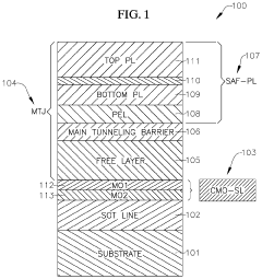
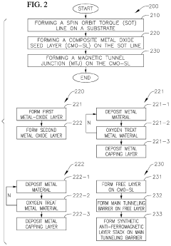
- The SOT-MRAM device incorporates a spin orbit torque line and a composite metal oxide seed layer beneath a magnetic tunnel junction, enabling efficient transverse spin-current transmission and interface perpendicular magnetic anisotropy for fast switching and data retention, with separate read/write paths.
Spin-orbit torque magnetic random-access memory(SOT-MRAM) device
PatentPendingKR1020240009333A
Innovation
- The introduction of a spin-orbit-torque magnetic random access memory (SOT-MRAM) device with a synthetic metal oxide seed layer and a spin-orbit torque line beneath the magnetic tunnel junction, which separates the read/write paths, utilizing materials like tantalum, tungsten, platinum, and hafnium to generate a transverse spin current for efficient switching and data retention.
Manufacturing Scalability of SOT-MRAM Technologies
The manufacturing scalability of SOT-MRAM technologies represents a critical factor in determining their commercial viability and widespread adoption. Current fabrication processes for SOT-MRAM face several challenges when transitioning from laboratory demonstrations to high-volume manufacturing environments. The integration of perpendicular magnetic anisotropy (PMA) materials with spin-orbit torque (SOT) mechanisms requires precise control over multiple thin film layers, often with thicknesses of just a few nanometers.
Key manufacturing challenges include maintaining consistent PMA quality across 300mm wafers while ensuring uniformity of the heavy metal/ferromagnet interfaces that generate the SOT effect. The industry has made significant progress in developing deposition techniques that can achieve the required atomic-level precision, with advanced sputtering and atomic layer deposition (ALD) methods showing promising results for maintaining interface quality at scale.
Thermal budget constraints present another significant hurdle, as PMA materials must maintain their magnetic properties throughout the CMOS back-end-of-line (BEOL) processing, which typically involves temperatures up to 400°C. Recent developments in thermally robust PMA materials, particularly CoFeB-MgO systems with added Ta, W, or Mo layers, have demonstrated improved stability during these thermal cycles, enhancing manufacturing compatibility.
Etching processes for SOT-MRAM structures require exceptional precision to avoid damaging the critical magnetic interfaces. Reactive ion etching (RIE) techniques have been refined to provide the necessary selectivity, though ion beam etching remains prevalent for critical magnetic stack patterning. The industry continues to develop specialized etching recipes that minimize sidewall damage while maintaining high throughput.
Integration with standard CMOS processes represents perhaps the most significant scaling challenge. Leading semiconductor manufacturers have demonstrated SOT-MRAM integration at the 22nm node and below, with roadmaps extending to 5nm and beyond. This integration requires careful consideration of materials compatibility, contamination control, and process module sequencing.
Yield management for SOT-MRAM manufacturing has improved substantially, with defect densities approaching those of conventional CMOS processes. Advanced metrology techniques, including magnetic force microscopy and time-resolved magneto-optical Kerr effect measurements, have been adapted for in-line quality control, enabling rapid identification of PMA variations and interface defects.
Cost considerations remain a factor in widespread adoption, though economies of scale are beginning to reduce the manufacturing premium associated with SOT-MRAM. As production volumes increase and process optimizations continue, the cost gap between SOT-MRAM and conventional memory technologies is narrowing, particularly when considering the performance and power advantages that SOT-MRAM offers for specific applications.
Energy Efficiency Considerations for SOT-MRAM Devices
Energy efficiency has emerged as a critical factor in the development and implementation of SOT-MRAM (Spin-Orbit Torque Magnetic Random Access Memory) devices, particularly those leveraging Perpendicular Magnetic Anisotropy (PMA) engineering. The power consumption profile of SOT-MRAM represents one of its most compelling advantages over conventional memory technologies, with significant implications for both mobile applications and data center infrastructures.
The fundamental energy efficiency of SOT-MRAM derives from its non-volatile nature, eliminating the need for constant power to maintain stored information. Current experimental SOT-MRAM devices with engineered PMA demonstrate write energies in the range of 0.1-1 pJ per bit, substantially lower than SRAM (1-2 pJ) and comparable to advanced DRAM implementations. Read operations typically consume an order of magnitude less energy than write operations, positioning SOT-MRAM as an exceptionally balanced memory solution.
PMA engineering directly impacts energy consumption through several mechanisms. Enhanced perpendicular anisotropy reduces the critical current density required for switching, resulting in lower power write operations. Recent advancements in interface engineering between the magnetic free layer and adjacent materials have demonstrated up to 40% reduction in switching current while maintaining thermal stability, representing a significant efficiency breakthrough.
The scaling properties of PMA-engineered SOT-MRAM further enhance its energy profile. As device dimensions decrease to sub-20nm nodes, properly engineered PMA structures maintain thermal stability while allowing proportionally lower switching currents, unlike in-plane anisotropy designs that face fundamental scaling limitations.
Material selection plays a crucial role in energy optimization. Heavy metal layers with strong spin-orbit coupling (such as Pt, W, and Ta) demonstrate varying degrees of charge-to-spin conversion efficiency. Recent work with topological insulators and 2D materials as SOT channels shows promise for achieving spin Hall angles exceeding 1.0, potentially reducing switching energy by an additional 30-50% compared to conventional heavy metal implementations.
Circuit-level considerations further impact overall system efficiency. The relatively high resistance of MTJ elements necessitates careful sense amplifier design to minimize read energy, while write driver circuits must balance current delivery capability with power consumption. Advanced architectures implementing local charge recycling techniques have demonstrated up to 25% reduction in effective write energy in laboratory settings.
Looking forward, the energy efficiency roadmap for SOT-MRAM with engineered PMA suggests potential for sub-0.1 pJ write operations within the next generation of devices, positioning this technology as a leading candidate for universal memory applications where both performance and energy constraints are critical considerations.
Unlock deeper insights with Patsnap Eureka Quick Research — get a full tech report to explore trends and direct your research. Try now!
Generate Your Research Report Instantly with AI Agent
Supercharge your innovation with Patsnap Eureka AI Agent Platform!