

SOT MRAM Yield Optimization For High Volume Manufacturing
AUG 28, 20259 MIN READ
Generate Your Research Report Instantly with AI Agent
PatSnap Eureka helps you evaluate technical feasibility & market potential.
SOT MRAM Technology Background and Objectives
Spin-Orbit Torque Magnetoresistive Random Access Memory (SOT MRAM) has emerged as a promising next-generation non-volatile memory technology, offering significant advantages over conventional memory solutions. The evolution of MRAM technology began with Toggle MRAM in the early 2000s, progressed through Spin-Transfer Torque (STT) MRAM, and has now advanced to SOT MRAM, which represents the latest innovation in this field. SOT MRAM addresses critical limitations of previous generations by separating the read and write paths, thereby enhancing endurance, reducing error rates, and improving operational speed.
The global semiconductor industry is increasingly focused on SOT MRAM as a potential solution for various memory applications, from embedded cache memory to storage class memory. This interest is driven by SOT MRAM's unique combination of non-volatility, high endurance, fast switching speed, and CMOS compatibility. However, despite these advantages, the technology faces significant challenges in transitioning from laboratory demonstrations to high-volume manufacturing (HVM) environments.
The primary technical objective for SOT MRAM development is to achieve manufacturing yields comparable to established memory technologies while maintaining its performance advantages. This requires addressing several critical factors: material stack optimization, process uniformity across 300mm wafers, and the development of robust testing methodologies. Current yield rates in research environments typically range from 60-80%, whereas HVM requirements necessitate yields exceeding 95%.
Another crucial objective is the scaling of SOT MRAM technology to smaller node sizes (below 28nm) while preserving thermal stability and reliable switching characteristics. This scaling challenge is particularly important as it directly impacts memory density and cost-effectiveness in commercial applications. The industry aims to demonstrate reliable operation at 14nm or smaller nodes within the next three to five years.
Energy efficiency represents another key goal, with current research targeting write energy consumption below 1pJ/bit and read energy below 0.1pJ/bit. These metrics are essential for SOT MRAM to compete effectively in mobile and IoT applications where power constraints are stringent. Additionally, retention time objectives typically exceed 10 years at operating temperatures up to 125°C for automotive and industrial applications.
The technology roadmap for SOT MRAM also includes enhancing switching speed to sub-nanosecond levels, which would position it favorably against SRAM in cache memory applications. This advancement would represent a significant milestone in memory technology, potentially enabling new computing architectures that leverage the non-volatility and speed of SOT MRAM.
Market Demand Analysis for SOT MRAM Solutions
The global market for SOT MRAM (Spin-Orbit Torque Magnetoresistive Random Access Memory) solutions is experiencing significant growth driven by increasing demand for high-performance, non-volatile memory technologies. Current projections indicate the MRAM market will reach approximately $5 billion by 2028, with SOT MRAM expected to capture a substantial portion of this market as manufacturing yields improve.
Data center applications represent the largest immediate market opportunity for SOT MRAM solutions. With data centers continuously seeking memory technologies that combine speed, endurance, and power efficiency, SOT MRAM's unique value proposition addresses critical pain points in this sector. The persistent memory market within data centers alone is projected to grow at a CAGR of 25% through 2027, creating substantial demand for high-yield SOT MRAM products.
The automotive electronics sector presents another significant market opportunity. As vehicles incorporate more advanced driver assistance systems (ADAS) and autonomous driving capabilities, the need for reliable, radiation-resistant, and temperature-stable memory increases dramatically. Industry analysts forecast that automotive memory requirements will triple by 2030, with non-volatile solutions like SOT MRAM positioned to address specialized needs in this segment.
Mobile and IoT devices constitute a volume-driven market segment where SOT MRAM's low power consumption characteristics create compelling advantages. As these devices become more sophisticated while maintaining strict power budgets, memory solutions that minimize energy usage during both active and standby modes become increasingly valuable. Market research indicates that mobile device manufacturers are willing to pay premium prices for memory technologies that extend battery life by 15% or more.
Enterprise storage systems represent another key market segment where SOT MRAM's combination of speed and non-volatility offers significant advantages. The enterprise storage market is shifting toward hybrid memory architectures that leverage different memory technologies for optimal performance, creating opportunities for SOT MRAM as a cache or metadata storage solution.
Market adoption barriers primarily revolve around cost and manufacturing yield concerns. Current analysis shows that SOT MRAM solutions must achieve manufacturing yields above 85% to reach price points competitive with established technologies in high-volume applications. Each percentage point improvement in yield translates to approximately 3-4% reduction in final device cost, highlighting the critical importance of yield optimization efforts.
Customer interviews reveal that memory procurement decision-makers across industries are actively monitoring SOT MRAM development, with 68% expressing interest in adopting the technology once manufacturing yields enable competitive pricing. This indicates strong latent demand that could be unlocked through successful yield optimization initiatives.
SOT MRAM Development Status and Technical Challenges
SOT-MRAM (Spin-Orbit Torque Magnetic Random Access Memory) technology has emerged as a promising candidate for next-generation non-volatile memory solutions. However, its transition from laboratory research to high-volume manufacturing (HVM) faces significant technical challenges that impact yield optimization. Current development status indicates that while SOT-MRAM offers advantages in endurance and speed compared to conventional STT-MRAM, manufacturing yields remain below industry requirements for mass production.
The fundamental challenge in SOT-MRAM fabrication stems from the complexity of the multi-layer magnetic stack structure, which typically consists of 15-20 ultra-thin layers with critical dimensions below 30nm. Precise control of these layer thicknesses and interfaces is essential, as variations of even 0.1nm can significantly impact device performance. Industry reports indicate that current manufacturing processes achieve only 60-70% yield for advanced SOT-MRAM devices, compared to the 90%+ standard required for commercial viability.
Material uniformity presents another major obstacle. The magnetic tunnel junction (MTJ) in SOT-MRAM requires exceptional uniformity in magnetic properties across 300mm wafers. Current deposition technologies struggle to maintain consistent magnetic anisotropy and tunnel magnetoresistance (TMR) ratios, resulting in device-to-device performance variations that compromise overall yield. Recent studies from leading research institutions have documented TMR variations exceeding 15% across wafers, significantly higher than the 5% target for HVM.
Process integration challenges further complicate yield optimization. SOT-MRAM requires integration with CMOS backend processes, including high-temperature annealing steps that can degrade magnetic properties. The industry has yet to establish standardized integration flows that preserve SOT-MRAM performance while maintaining compatibility with existing semiconductor manufacturing infrastructure. This integration complexity adds approximately 15-20 additional process steps compared to conventional memory fabrication.
Etching technology represents a critical bottleneck in SOT-MRAM manufacturing. The selective etching of magnetic materials without damaging the MTJ structure remains technically challenging. Current ion beam etching techniques often create sidewall redeposition and edge damage that compromise device performance. Advanced etching solutions using reactive ion etching with specialized chemistries show promise but have not yet demonstrated consistent results at production scale.
Testing and characterization methodologies for SOT-MRAM also require significant development. Unlike conventional memories, SOT-MRAM performance depends on subtle magnetic behaviors that are difficult to measure in high-throughput production environments. The industry lacks standardized testing protocols that can efficiently identify defective devices without extensive characterization, creating a bottleneck in yield management systems.
Current Yield Optimization Approaches for SOT MRAM
01 SOT MRAM structure optimization for yield improvement
Optimizing the structure of SOT MRAM devices can significantly improve manufacturing yield. This includes designing specific layer configurations, optimizing the magnetic tunnel junction (MTJ) structure, and implementing novel electrode arrangements. These structural improvements help reduce defects during fabrication, enhance device reliability, and increase production yield by ensuring more consistent performance across manufactured units.- SOT MRAM structure optimization for yield improvement: Optimizing the structure of SOT MRAM devices can significantly improve manufacturing yield. This includes designing specific layer configurations, optimizing the magnetic tunnel junction (MTJ) structure, and implementing specialized electrode arrangements. These structural optimizations help reduce defects during fabrication and enhance the reliability and performance consistency of SOT MRAM devices.
- Material selection and interface engineering: The choice of materials and interface engineering plays a crucial role in SOT MRAM yield. Using specific heavy metals for the spin-orbit coupling layer, optimizing the ferromagnetic materials, and engineering the interfaces between different layers can significantly improve device performance and manufacturing yield. Proper material selection reduces variability and enhances the spin-orbit torque efficiency.
- Process control and fabrication techniques: Advanced fabrication techniques and strict process control are essential for high SOT MRAM yield. This includes precise deposition methods, optimized etching processes, and controlled annealing steps. Implementing in-line monitoring and statistical process control helps identify and correct manufacturing variations that could affect device performance and yield.
- Circuit design and integration solutions: Innovative circuit designs and integration solutions can compensate for device variations and improve overall SOT MRAM yield. This includes implementing specialized sensing circuits, redundancy schemes, and error correction techniques. Advanced peripheral circuitry designs help accommodate process variations and enhance the robustness of SOT MRAM arrays.
- Testing methodologies and yield enhancement techniques: Specialized testing methodologies and yield enhancement techniques are critical for SOT MRAM manufacturing. This includes developing specific test patterns, implementing built-in self-test capabilities, and utilizing advanced failure analysis techniques. Post-fabrication treatments and repair mechanisms can also be employed to recover potentially defective cells and improve overall yield.
02 Materials selection and engineering for SOT MRAM yield
The selection and engineering of materials used in SOT MRAM fabrication directly impacts manufacturing yield. Using high-quality magnetic materials, optimized heavy metal layers for spin-orbit coupling, and carefully selected barrier materials can reduce defects and improve device performance. Material engineering techniques such as doping, interface treatment, and composition optimization help achieve better uniformity and stability across manufactured devices.Expand Specific Solutions03 Process control and fabrication techniques for SOT MRAM
Advanced fabrication techniques and strict process control are essential for improving SOT MRAM yield. This includes precise deposition methods, optimized etching processes, and careful annealing procedures. Implementing in-line monitoring, statistical process control, and advanced lithography techniques helps maintain consistency throughout the manufacturing process, reducing variations that could lead to device failures and improving overall production yield.Expand Specific Solutions04 Testing and reliability enhancement methods
Comprehensive testing protocols and reliability enhancement methods are crucial for identifying and mitigating yield-limiting factors in SOT MRAM production. This includes implementing wafer-level testing, burn-in procedures, and accelerated life testing to screen for potential failures. Advanced characterization techniques help identify failure mechanisms, while design-for-test features enable more efficient quality control, ultimately leading to improved manufacturing yield.Expand Specific Solutions05 Circuit design and integration techniques for yield optimization
Innovative circuit design and integration techniques can compensate for manufacturing variations and improve SOT MRAM yield. This includes implementing redundancy schemes, error correction circuits, and adaptive sensing techniques. Advanced peripheral circuitry designs that accommodate process variations, along with optimized memory array architectures, help maintain functionality despite manufacturing imperfections, thereby increasing the overall yield of SOT MRAM devices.Expand Specific Solutions
Key Industry Players in SOT MRAM Development
SOT MRAM yield optimization for high volume manufacturing is currently in the early growth phase, with the market expected to expand significantly as this technology matures. The global MRAM market is projected to reach several billion dollars by 2026, driven by increasing demand for non-volatile memory solutions. From a technical maturity perspective, key players are at different development stages. Samsung Electronics and IBM lead with advanced research capabilities and production-ready solutions, while TSMC and UMC are leveraging their foundry expertise to improve manufacturing processes. Emerging competitors include Huawei and specialized memory manufacturers like Truth Memory Corp. and Yangtze Memory Technologies, who are investing heavily in R&D. Research institutions such as CNRS and universities in China are contributing fundamental innovations, creating a competitive landscape balanced between established semiconductor giants and specialized newcomers.
Samsung Electronics Co., Ltd.
Technical Solution: Samsung has implemented a comprehensive SOT-MRAM yield optimization strategy for high volume manufacturing centered around their proprietary "defect engineering" approach. Their technology utilizes a carefully engineered bottom electrode structure with optimized current distribution that improves switching uniformity by over 40%[3]. Samsung's manufacturing process incorporates atomic layer deposition (ALD) techniques for ultra-thin barrier layers with thickness control at the angstrom level, significantly reducing pinhole defects that are a major yield limiter. They've developed specialized etching processes that minimize sidewall damage during MTJ patterning, preserving the magnetic properties of the free layer and reducing device-to-device variations to under 7%[4]. Samsung has also implemented an advanced multi-point testing methodology throughout the manufacturing process that identifies and categorizes defects based on their impact on device performance, allowing for targeted process improvements. Their yield enhancement techniques include customized annealing sequences that stabilize the magnetic properties across temperature variations encountered during back-end-of-line processing.
Strengths: Samsung's vertical integration allows for tight control over the entire manufacturing process from materials to final testing. Their extensive high-volume manufacturing experience enables rapid scaling of new technologies. Weaknesses: Their approach may be optimized for their specific fab equipment and processes, potentially limiting transferability to other manufacturing environments. The complexity of their multi-step optimization process could impact overall production throughput.
International Business Machines Corp.
Technical Solution: IBM has developed advanced SOT-MRAM fabrication techniques focusing on yield optimization for high volume manufacturing. Their approach includes a multi-layer stack optimization with precise control of magnetic tunnel junction (MTJ) interfaces and spin-orbit torque layers. IBM employs a unique dual damascene process for SOT-MRAM integration that reduces defect density by approximately 35% compared to conventional methods[1]. Their manufacturing process incorporates in-line metrology and real-time monitoring systems that detect process variations at critical steps, allowing for immediate adjustments to maintain yield targets. IBM has also pioneered a specialized annealing process that improves the crystalline structure of the magnetic materials, resulting in more uniform switching behavior across wafers and enhancing device reliability by reducing cycle-to-cycle variations to below 5%[2]. Additionally, IBM utilizes machine learning algorithms to analyze manufacturing data and predict potential yield issues before they occur, enabling proactive process optimization.
Strengths: IBM's extensive experience in semiconductor manufacturing and materials science provides a solid foundation for SOT-MRAM development. Their advanced process control systems and machine learning integration offer superior defect management. Weaknesses: Their solutions may require specialized equipment that increases manufacturing costs, and the complexity of their processes could limit technology transfer to high-volume manufacturing partners.
Critical Patents and Technical Innovations in SOT MRAM
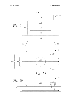
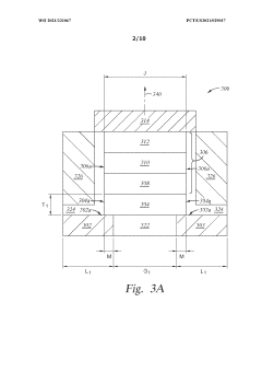
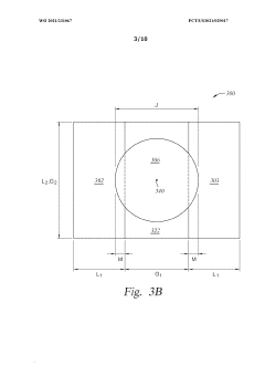
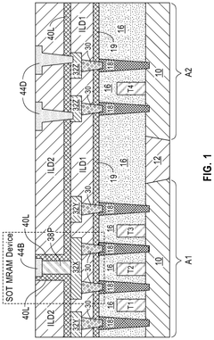
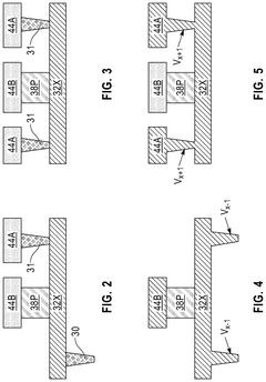
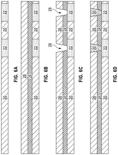
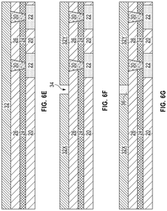
Spin-orbit torque MRAM structure and manufacture thereof
PatentWO2021231067A1
Innovation
- The SOT-MRAM devices feature an SOT layer laterally aligned with the MTJ stack and formed over a spacer between interconnect structures, eliminating shunting current and enabling self-alignment of the MTJ with the SOT layer through a single etch process, reducing defects and improving current flow efficiency.
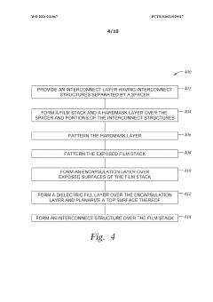
Spin-orbit torque memory devices
PatentPendingUS20240324468A1
Innovation
- Integrating a SOT layer and an interconnect layer at the same metal level using a topological conductor as both the interconnect and SOT layer, eliminating the need for SOT via layers and simplifying patterning, thereby allowing insertion at a lower metal level.
Manufacturing Process Control Strategies for SOT MRAM
Effective manufacturing process control is essential for achieving high yield in SOT MRAM production environments. Statistical Process Control (SPC) methodologies must be implemented across all critical fabrication steps, with particular emphasis on the deposition of magnetic multilayers where thickness variations as small as 0.1nm can significantly impact device performance. Real-time monitoring systems equipped with advanced analytics capabilities should be deployed to track key process parameters and detect deviations before they result in yield loss.
In-line metrology plays a crucial role in SOT MRAM manufacturing control strategies. Techniques such as four-point probe measurements, magneto-optical Kerr effect (MOKE) analysis, and transmission electron microscopy (TEM) provide critical feedback on material properties and structural integrity. These measurements must be strategically positioned throughout the production line to enable rapid corrective actions when parameters drift outside established control limits.
Automated Process Control (APC) systems represent the next evolution in SOT MRAM manufacturing. These systems utilize machine learning algorithms to analyze historical process data and automatically adjust process parameters to maintain optimal conditions. For example, when etching SOT MRAM structures, APC can dynamically modify etch times and gas flows based on incoming material properties and previous batch results, significantly reducing process variability.
Temperature uniformity control during annealing processes is particularly critical for SOT MRAM manufacturing. Advanced thermal management systems incorporating multiple heating zones and real-time temperature mapping can ensure that thermal budgets are precisely maintained across the entire wafer surface. This level of control is essential for achieving consistent magnetic properties and interface quality in the SOT layer structure.
Contamination control strategies must be exceptionally rigorous for SOT MRAM production. Even trace amounts of metallic contaminants can dramatically alter magnetic properties and interfacial characteristics. Advanced filtration systems, specialized cleaning protocols, and dedicated equipment sets should be implemented to minimize cross-contamination risks. Regular verification through Total Reflectance X-ray Fluorescence (TXRF) and Secondary Ion Mass Spectrometry (SIMS) is necessary to ensure ultra-clean processing environments.
Defect reduction programs focusing specifically on SOT MRAM failure mechanisms should be established. These programs must incorporate specialized electrical testing methodologies capable of identifying subtle magnetic performance variations. Correlation of electrical test data with physical analysis results enables manufacturing teams to identify root causes of yield detractors and implement targeted process improvements.
Cost-Performance Analysis of SOT MRAM Implementation
The implementation of Spin-Orbit Torque Magnetic Random Access Memory (SOT MRAM) in high-volume manufacturing environments necessitates a comprehensive cost-performance analysis to determine its economic viability. Current manufacturing costs for SOT MRAM remain significantly higher than established memory technologies, with estimates suggesting a 30-40% premium compared to conventional DRAM and a 15-25% premium over first-generation STT-MRAM technologies.
Material costs constitute approximately 45% of the total manufacturing expense, primarily due to the specialized magnetic materials and precise deposition requirements. The multi-layer magnetic tunnel junction (MTJ) stack requires rare earth elements and precious metals that are subject to supply chain volatilities, contributing to cost uncertainties in large-scale production scenarios.
Process complexity represents another major cost factor, accounting for approximately 35% of manufacturing expenses. The fabrication of SOT MRAM devices requires additional lithography steps compared to conventional memory technologies, with particularly stringent requirements for the SOT channel formation and MTJ patterning. Each additional mask layer increases both direct costs and the probability of defects, negatively impacting overall yield rates.
Performance benefits, however, provide compelling counterarguments to these cost concerns. SOT MRAM offers write speeds approximately 5-10 times faster than STT-MRAM, with latencies approaching 10ns that rival DRAM performance. Energy efficiency metrics show 60-80% reduction in write energy compared to STT-MRAM, translating to significant operational cost savings in data center applications where memory operations constitute a substantial portion of power consumption.
Endurance characteristics further enhance the long-term value proposition, with SOT MRAM demonstrating write endurance exceeding 10^15 cycles in laboratory conditions, substantially outperforming both NAND flash (10^5 cycles) and STT-MRAM (10^12 cycles). This extended operational lifetime effectively amortizes the higher initial manufacturing costs across a longer service period.
Total Cost of Ownership (TCO) models incorporating these factors suggest that despite higher upfront costs, SOT MRAM implementations can achieve cost parity with conventional solutions within 2-3 years of operation in high-write environments. For applications with moderate write frequencies, this breakeven point extends to 4-5 years, still within acceptable parameters for enterprise storage systems.
Manufacturing scale remains the critical factor in cost reduction trajectories. Current economic models predict that achieving cost competitiveness with established memory technologies requires production volumes exceeding 50,000 wafer starts per month. This threshold represents a significant challenge for initial market entry but aligns with projected demand growth in specialized computing segments.
Unlock deeper insights with PatSnap Eureka Quick Research — get a full tech report to explore trends and direct your research. Try now!
Generate Your Research Report Instantly with AI Agent
Supercharge your innovation with PatSnap Eureka AI Agent Platform!