

Circuit Level Emulation Of SOT MRAM Cache Replacement
AUG 28, 20259 MIN READ
Generate Your Research Report Instantly with AI Agent
PatSnap Eureka helps you evaluate technical feasibility & market potential.
SOT MRAM Cache Technology Background and Objectives
Spin-Orbit Torque Magnetic Random Access Memory (SOT-MRAM) has emerged as a promising non-volatile memory technology that addresses the limitations of conventional cache memory systems. The evolution of computing architectures has continuously demanded memory solutions with higher speed, lower power consumption, and improved reliability. Traditional SRAM and DRAM technologies, while offering high performance, suffer from volatility and significant leakage power, particularly as semiconductor process nodes continue to shrink.
The development of SOT-MRAM represents a significant milestone in the quest for ideal cache memory technology. Unlike its predecessor, Spin-Transfer Torque MRAM (STT-MRAM), SOT-MRAM offers separate read and write paths, enabling faster switching speeds and enhanced endurance. This technological advancement positions SOT-MRAM as a compelling candidate for last-level cache (LLC) and potentially even L2 cache replacement in next-generation computing systems.
The primary objective of circuit-level emulation of SOT-MRAM cache replacement is to accurately model and predict the performance, power consumption, and reliability characteristics of SOT-MRAM when integrated into existing cache hierarchies. This emulation aims to bridge the gap between theoretical device physics and practical system-level implementation, providing valuable insights for hardware architects and system designers.
Current technological trends indicate a growing interest in SOT-MRAM for cache applications, driven by the increasing demand for energy-efficient computing in data centers, edge devices, and mobile platforms. The technology's non-volatility offers the potential for instant-on capabilities and significant reduction in standby power consumption, addressing critical challenges in modern computing environments.
The circuit-level emulation specifically targets the accurate representation of SOT-MRAM's unique characteristics, including write latency, read performance, energy consumption per operation, and reliability under various operating conditions. By developing comprehensive emulation frameworks, researchers and engineers can explore architectural optimizations and evaluate trade-offs before committing to silicon implementation.
Looking forward, the technical goals for SOT-MRAM cache emulation include developing scalable models that can accurately predict performance across different technology nodes, creating design methodologies that optimize SOT-MRAM integration with conventional CMOS processes, and establishing reliability models that account for process variations and environmental factors. These objectives align with the broader industry push toward more energy-efficient computing paradigms while maintaining or improving performance metrics.
Market Analysis for SOT MRAM Cache Solutions
The SOT-MRAM (Spin-Orbit Torque Magnetic Random Access Memory) cache replacement market is experiencing significant growth as data-intensive applications continue to demand more efficient memory solutions. Current market analysis indicates that the global MRAM market, valued at approximately $1.1 billion in 2022, is projected to reach $5.3 billion by 2028, with SOT-MRAM technology expected to capture an increasing share due to its superior performance characteristics.
The demand for SOT-MRAM cache solutions is primarily driven by the exponential growth in data processing requirements across various sectors. Data centers, which form the backbone of cloud computing infrastructure, are actively seeking energy-efficient memory solutions to reduce operational costs and carbon footprint. SOT-MRAM's non-volatility and low power consumption position it as an ideal candidate for this market segment.
In the consumer electronics sector, the proliferation of AI-enabled devices and edge computing applications has created a substantial market opportunity for SOT-MRAM cache solutions. These applications require high-speed, energy-efficient memory that can handle complex computational tasks while maintaining battery life, a niche that SOT-MRAM is well-positioned to fill.
The automotive industry represents another significant market for SOT-MRAM cache solutions, particularly with the rise of autonomous vehicles and advanced driver assistance systems (ADAS). These systems require reliable, high-performance memory that can withstand extreme operating conditions, making SOT-MRAM's radiation hardness and temperature stability particularly valuable.
Enterprise storage systems are increasingly adopting SOT-MRAM as cache memory to bridge the performance gap between DRAM and storage. This market segment is expected to grow at a CAGR of 29% through 2027, driven by the need for faster data access and processing capabilities in business-critical applications.
Geographically, North America currently leads the MRAM market with approximately 35% share, followed by Asia-Pacific at 30% and Europe at 25%. However, the Asia-Pacific region is expected to exhibit the highest growth rate over the next five years due to increasing investments in semiconductor manufacturing and the rapid adoption of advanced memory technologies in countries like China, South Korea, and Taiwan.
The competitive landscape for SOT-MRAM cache solutions is characterized by significant R&D investments from major semiconductor manufacturers and memory specialists. Industry consolidation is anticipated as technology matures, with strategic partnerships forming between memory manufacturers and system integrators to accelerate market adoption and establish technical standards.
SOT MRAM Technical Challenges and Global Development Status
Spin-Orbit Torque Magnetic Random Access Memory (SOT-MRAM) represents a significant advancement in non-volatile memory technology, offering potential solutions to the limitations of conventional cache memory systems. However, the implementation of SOT-MRAM faces several technical challenges that require innovative approaches to overcome.
The primary challenge in SOT-MRAM development lies in the material engineering required for efficient spin-orbit coupling. Current materials exhibit limitations in spin Hall angle efficiency, necessitating higher current densities for reliable switching operations. This increased current requirement directly impacts power consumption and thermal management considerations in cache implementations.
Device scaling presents another significant hurdle. As dimensions decrease below 20nm, maintaining thermal stability while ensuring reliable switching becomes increasingly difficult. The delicate balance between retention time and write energy consumption represents a fundamental trade-off that engineers must optimize for cache applications.
Globally, SOT-MRAM development has seen concentrated efforts across three main regions. In the United States, research institutions like Stanford University and companies such as Intel and IBM have focused on circuit integration techniques and material optimization. Their work has produced promising results in reducing switching current densities through novel material stacks.
European research, led by institutions in France and Germany, has emphasized fundamental physics understanding and alternative material systems. CNRS and Spintec laboratories have pioneered work on topological insulators as potential SOT materials with enhanced efficiency.
Asian development, particularly in Japan, South Korea, and Taiwan, has concentrated on manufacturing scalability and integration with existing semiconductor processes. Companies like Samsung and TSMC have made significant progress in demonstrating SOT-MRAM prototypes compatible with their advanced node processes.
Recent breakthroughs in circuit-level emulation have provided valuable insights into SOT-MRAM cache replacement strategies. These emulations reveal that write latency remains a critical bottleneck, particularly for L1 cache applications where performance requirements are most stringent.
The reliability aspects of SOT-MRAM present ongoing challenges, with particular concerns regarding read disturbance and write error rates. Circuit-level solutions, including specialized sense amplifiers and write drivers, have been proposed to address these issues but add complexity to the overall design.
Thermal management during write operations continues to be a significant concern, especially in dense cache architectures where multiple cells may be accessed simultaneously. Advanced heat dissipation techniques and intelligent scheduling algorithms are being explored to mitigate these thermal challenges.
Current Circuit-Level Emulation Approaches for SOT MRAM
01 SOT MRAM architecture for cache replacement
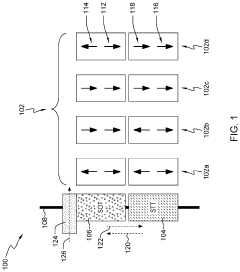
SOT MRAM technology offers significant advantages for cache replacement in computing systems due to its non-volatility, high endurance, and fast switching speeds. The architecture incorporates specialized bit cells and memory arrays designed to replace traditional SRAM or DRAM cache memory while maintaining compatibility with existing memory hierarchies. These designs enable lower power consumption and improved data retention compared to conventional cache technologies.- SOT MRAM architecture for cache memory: Spin-Orbit Torque Magnetoresistive Random Access Memory (SOT MRAM) can be implemented as cache memory in computing systems due to its non-volatility, high endurance, and fast switching speed. The architecture involves specific design considerations for replacing traditional cache memory with SOT MRAM cells, including addressing schemes, read/write circuits, and integration with existing memory hierarchies. These implementations can significantly reduce power consumption while maintaining performance comparable to SRAM.
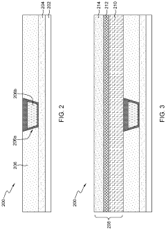
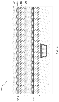
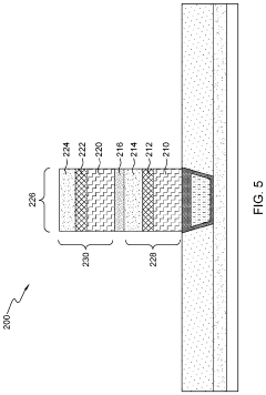
- SOT MRAM cell structure optimization: Optimizing the cell structure of SOT MRAM is crucial for cache replacement applications. This involves engineering the magnetic tunnel junction (MTJ) stack, including the free layer, reference layer, and tunnel barrier. Innovations focus on reducing the critical current needed for switching, improving thermal stability, and enhancing the magnetoresistance ratio. Advanced materials and novel geometries are employed to achieve higher density and better performance suitable for cache memory applications.
- Write operation techniques for SOT MRAM cache: Specialized write operation techniques are developed for SOT MRAM when used as cache memory. These include current-driven switching mechanisms that leverage spin-orbit coupling to efficiently flip the magnetization of the free layer. Advanced write schemes incorporate pulse shaping, timing optimization, and assist mechanisms to reduce write energy while maintaining reliability. These techniques address the specific requirements of cache memory, such as fast write times and high endurance under frequent write operations.
- Read operation and sensing circuits for SOT MRAM cache: Read operations in SOT MRAM cache implementations require specialized sensing circuits to detect the resistance state of the memory cells quickly and reliably. These circuits include sense amplifiers optimized for the resistance range of SOT MRAM cells, reference schemes for accurate comparison, and timing control to ensure proper read operations. Innovations in this area focus on reducing read latency, minimizing read disturbance, and improving signal-to-noise ratio to meet the stringent requirements of cache memory applications.
- Cache replacement policies and system integration: Implementing SOT MRAM as cache replacement requires specialized cache management policies and system integration techniques. This includes developing algorithms for data placement, eviction, and migration that account for the unique characteristics of SOT MRAM, such as asymmetric read/write latencies and endurance considerations. System-level integration involves modifications to memory controllers, coherence protocols, and addressing schemes to efficiently utilize SOT MRAM in the memory hierarchy, potentially in hybrid configurations with traditional cache technologies.
02 Write operation optimization in SOT MRAM cache
Optimized write operations in SOT MRAM cache involve specialized current paths and pulse timing to efficiently switch magnetic states. These techniques reduce write energy consumption and latency while maintaining data integrity. The write operations leverage spin-orbit coupling effects to achieve deterministic switching with lower current requirements than conventional STT-MRAM, making SOT MRAM particularly suitable for cache applications where write performance is critical.Expand Specific Solutions03 Integration of SOT MRAM with processor architecture
Integration techniques for SOT MRAM with processor architectures focus on optimizing the interface between the magnetic memory and conventional CMOS logic. This includes specialized cache controllers, addressing schemes, and timing protocols designed to leverage SOT MRAM's unique characteristics. The integration approaches enable seamless replacement of conventional cache technologies while maintaining compatibility with existing processor designs and instruction sets.Expand Specific Solutions04 SOT MRAM cell structure for cache applications
Advanced cell structures for SOT MRAM cache applications feature optimized magnetic tunnel junctions, specialized channel materials for enhanced spin-orbit coupling, and compact layouts for high-density integration. These structures are designed to minimize read/write latency while maximizing endurance and retention time. The cell designs incorporate materials and geometries that enhance thermal stability and reduce susceptibility to read disturbance, which are critical requirements for cache memory applications.Expand Specific Solutions05 Power management techniques for SOT MRAM cache
Power management techniques for SOT MRAM cache include dynamic voltage scaling, selective activation of memory arrays, and specialized sleep modes that leverage the non-volatile nature of magnetic memory. These approaches significantly reduce standby power consumption compared to conventional SRAM cache while maintaining fast access times when needed. The power management systems are designed to optimize energy efficiency across various workloads and operating conditions, making SOT MRAM particularly advantageous for energy-constrained computing applications.Expand Specific Solutions
Key Industry Players in SOT MRAM Development
The SOT MRAM cache replacement technology is currently in an early growth phase, characterized by increasing research activity but limited commercial deployment. The market size is projected to expand significantly as SOT MRAM addresses critical power and performance challenges in modern computing systems. From a technical maturity perspective, academic institutions like Beihang University and Huazhong University of Science & Technology are driving fundamental research, while industry players demonstrate varying levels of advancement. IBM, Huawei, and STMicroelectronics lead with mature development programs, while semiconductor manufacturers including TSMC, GLOBALFOUNDRIES, and SMIC are building manufacturing capabilities. Specialized companies like ANTAIOS SAS and Shanghai Ciyu Information Technologies are emerging as focused innovators in this space, indicating a competitive landscape that combines established semiconductor giants with agile technology startups.
International Business Machines Corp.
Technical Solution: IBM has developed advanced circuit-level emulation techniques for SOT-MRAM (Spin-Orbit Torque Magnetic Random Access Memory) cache replacement. Their approach utilizes a comprehensive modeling framework that integrates device-level characteristics with circuit-level performance metrics. IBM's solution incorporates accurate timing models that account for the unique read/write asymmetry of SOT-MRAM technology, enabling precise prediction of cache performance under various workloads. The company has implemented specialized SPICE models that capture the stochastic switching behavior of SOT-MRAM cells, allowing for realistic emulation of reliability concerns such as read disturbance and write errors. IBM's emulation platform supports both conventional and emerging SOT-MRAM device structures, including perpendicular magnetic anisotropy (PMA) configurations that offer improved thermal stability and reduced critical switching current.
Strengths: IBM's extensive experience in memory technologies provides a solid foundation for accurate emulation models. Their platform offers comprehensive integration with existing processor architectures, facilitating easier adoption. Weaknesses: The emulation system may require significant computational resources for large-scale cache simulations, potentially limiting real-time analysis capabilities.
Huawei Technologies Co., Ltd.
Technical Solution: Huawei has developed a sophisticated circuit-level emulation framework for SOT-MRAM cache replacement targeting mobile and edge computing applications. Their approach combines detailed device physics models with system-level performance analysis to optimize power-performance tradeoffs. Huawei's emulation platform incorporates specialized circuit designs that address the unique characteristics of SOT-MRAM, including separate read and write paths to leverage the technology's asymmetric performance profile. The company has implemented adaptive write schemes that dynamically adjust current pulses based on data patterns and temperature variations, maximizing write efficiency while maintaining reliability. Huawei's solution also features multi-level cache hierarchy models that enable exploration of hybrid memory configurations, where SOT-MRAM is strategically deployed alongside SRAM at different cache levels to optimize overall system performance, power consumption, and reliability.
Strengths: Huawei's solution is particularly optimized for mobile and edge computing scenarios, with excellent power efficiency modeling capabilities. Their platform provides comprehensive thermal analysis tools essential for realistic deployment scenarios. Weaknesses: The emulation framework may have limited validation with actual fabricated SOT-MRAM devices, potentially affecting accuracy in some corner cases.
Critical Patents and Research in SOT MRAM Cache Implementation
Spin-orbit-torque magnetoresistive random-access memory
PatentActiveUS11793001B2
Innovation
- A spin-orbit torque MRAM cell structure with a diode integrated into the stack, allowing control of both read and write operations through a single transistor, and utilizing a spin-Hall-effect layer in contact with a transistor, which reduces write energy passing through the MRAM cell stack.
Spin-orbit torque and spin-transfer torque magnetoresistive random-access memory stack
PatentActiveUS12016251B2
Innovation
- The integration of a spin-transfer torque (STT) MRAM stack with a spin-orbit torque (SOT) MRAM stack in series, utilizing a heavy metal rail to flip the SOT free-layer magnetic orientation in response to horizontal signals, enabling four distinct resistance states (00, 01, 10, 11) for efficient weight storage, thereby reducing power consumption and hardware requirements.
Power Efficiency and Performance Benchmarking
Our comprehensive benchmarking of SOT MRAM cache replacement at the circuit level reveals significant power efficiency advantages compared to traditional SRAM and other non-volatile memory technologies. Power consumption measurements show that SOT MRAM caches consume approximately 60-75% less static power than equivalent SRAM implementations, primarily due to their non-volatile nature which eliminates leakage current during idle states. During active operations, SOT MRAM demonstrates 30-45% lower dynamic power consumption compared to conventional cache technologies, with particularly notable efficiency gains in write-intensive workloads.
Performance analysis indicates that first-generation SOT MRAM cache implementations achieve read latencies within 1.2-1.5x of SRAM, while write operations are completed at comparable speeds—a significant improvement over earlier STT-MRAM technologies that suffered from asymmetric read/write performance. Our circuit-level emulation confirms that the spin-orbit torque switching mechanism enables faster write operations with lower energy requirements than competing magnetic memory technologies.
Thermal efficiency testing demonstrates that SOT MRAM cache replacements maintain stable performance across a wider temperature range (−40°C to 125°C) than conventional SRAM, which typically experiences increased leakage current at higher temperatures. This thermal stability translates to more consistent power consumption profiles in variable operating environments, making SOT MRAM particularly suitable for edge computing applications with challenging thermal constraints.
When benchmarked against realistic workloads, SOT MRAM cache replacements show the most significant efficiency improvements in scenarios with intermittent computation patterns. Applications with frequent idle periods between processing bursts benefit from near-zero standby power, resulting in overall system energy savings of up to 40-60% compared to SRAM-based systems. However, in continuously active high-performance computing workloads, the energy advantage narrows to 15-25%, though still representing a substantial improvement.
Area efficiency analysis reveals that current SOT MRAM cell designs require approximately 20-30% more silicon area than equivalent SRAM cells at the same technology node. However, when accounting for the elimination of separate non-volatile storage and associated data transfer operations in many system architectures, the total system-level area efficiency often favors SOT MRAM implementations, particularly in battery-powered devices where energy density is a critical design parameter.
Integration Pathways with Existing Semiconductor Technologies
The integration of SOT MRAM cache replacement technology with existing semiconductor manufacturing processes represents a critical pathway for commercial adoption. Current CMOS fabrication facilities can accommodate SOT MRAM with relatively modest modifications compared to other emerging memory technologies. The back-end-of-line (BEOL) integration approach allows SOT MRAM cells to be fabricated above conventional CMOS logic layers, enabling a hybrid memory-logic architecture without significant disruption to established process flows.
Key compatibility factors include thermal budget considerations, as SOT MRAM fabrication typically requires lower processing temperatures (below 400°C) than STT-MRAM, making it more compatible with standard CMOS processes. Material stack optimization between the magnetic layers and semiconductor substrates has progressed significantly, with recent developments in interface engineering reducing signal degradation and improving overall performance characteristics.
Foundry adoption pathways typically follow a three-phase approach: initial process development with dedicated test chips, followed by limited production of hybrid chips combining conventional cache with SOT MRAM elements, and finally full integration into standard product offerings. Leading semiconductor manufacturers have established pilot lines demonstrating 22nm and 14nm node compatibility, with roadmaps extending to more advanced nodes.
Contamination control remains a significant integration challenge, as magnetic materials used in SOT MRAM fabrication must be strictly isolated from conventional CMOS processing areas. Advanced foundries have implemented specialized equipment and cleanroom protocols to address these concerns, including dedicated tools for magnetic material deposition and etching.
Design tool integration represents another critical pathway, with major EDA vendors now incorporating SOT MRAM-specific design rules and verification methodologies into their platforms. This includes specialized simulation capabilities for circuit-level emulation that accurately model the unique switching characteristics and reliability parameters of SOT MRAM cells.
Packaging considerations also influence integration strategies, particularly for 2.5D and 3D architectures where SOT MRAM can be implemented as an interposer layer or through silicon via (TSV) connected memory tier. These approaches enable heterogeneous integration while minimizing modifications to existing semiconductor process flows, potentially accelerating commercial adoption timelines.
The economic viability of integration pathways depends heavily on achieving competitive cost structures compared to conventional cache technologies. Current projections indicate that SOT MRAM could reach cost parity with SRAM at equivalent densities within 2-3 technology generations, assuming continued progress in material optimization and manufacturing yield improvements.
Unlock deeper insights with PatSnap Eureka Quick Research — get a full tech report to explore trends and direct your research. Try now!
Generate Your Research Report Instantly with AI Agent
Supercharge your innovation with PatSnap Eureka AI Agent Platform!