Effect Of Grain Structure On SOT Layer Performance
AUG 28, 20259 MIN READ
Generate Your Research Report Instantly with AI Agent
Patsnap Eureka helps you evaluate technical feasibility & market potential.
SOT Technology Background and Objectives
Spin-Orbit Torque (SOT) technology has emerged as a promising approach for next-generation magnetic memory and logic devices, offering advantages in energy efficiency, speed, and endurance compared to conventional spin-transfer torque (STT) mechanisms. The fundamental principle behind SOT relies on the conversion of charge current to spin current through spin-orbit coupling effects in heavy metal or topological insulator layers adjacent to ferromagnetic materials.
The evolution of SOT technology can be traced back to early theoretical predictions in the 2000s, followed by experimental demonstrations around 2010 that verified the ability to manipulate magnetic moments using SOT. Since then, research has intensified significantly, with major breakthroughs occurring in materials engineering, device architecture, and understanding of underlying physical mechanisms.
Current SOT research focuses on optimizing the efficiency of charge-to-spin conversion, reducing critical switching currents, and enhancing thermal stability. The grain structure of SOT layers has emerged as a critical factor affecting these performance metrics, as it directly influences spin diffusion length, interface quality, and magnetization dynamics.
The microstructural characteristics of SOT layers, including grain size distribution, crystallographic orientation, and grain boundary properties, significantly impact spin transport phenomena. Recent studies have demonstrated that controlling grain structure through deposition conditions, annealing processes, and material composition can lead to substantial improvements in SOT efficiency.
The primary technical objectives in this field include achieving deterministic switching with minimal energy consumption, enhancing thermal stability for reliable data retention, and ensuring compatibility with CMOS fabrication processes for seamless integration into existing semiconductor manufacturing workflows.
Industry roadmaps project SOT-based devices as potential replacements for conventional MRAM technologies, particularly in applications requiring ultra-fast operation and high endurance. The technology is expected to enable new computing paradigms, including neuromorphic computing and in-memory processing architectures.
Understanding and controlling the relationship between grain structure and SOT performance represents a crucial step toward commercial viability. This requires interdisciplinary approaches combining materials science, spintronics, and device engineering to develop predictive models and design guidelines for optimized SOT layers.
The ultimate goal is to establish clear correlations between processing parameters, resulting grain structures, and device performance metrics, enabling systematic optimization of SOT-based technologies for next-generation computing systems and memory applications.
Market Analysis for SOT-based Devices
The global market for SOT (Spin-Orbit Torque) based devices is experiencing significant growth, driven by increasing demands for more efficient and faster memory solutions. Current projections indicate the SOT-MRAM market could reach approximately $2 billion by 2028, with a compound annual growth rate exceeding 40% from 2023 to 2028. This remarkable growth trajectory is primarily fueled by the expanding applications in data centers, automotive electronics, and IoT devices where non-volatility, speed, and endurance are critical requirements.
The enterprise storage sector represents the largest market segment for SOT-based devices, accounting for nearly 45% of the total addressable market. This dominance stems from the increasing need for high-performance, energy-efficient storage solutions in data centers facing exponential growth in data processing demands. The automotive sector follows as the second-largest market, driven by the rapid adoption of advanced driver-assistance systems and autonomous driving technologies requiring reliable, high-speed memory components that can operate in extreme conditions.
Geographically, North America currently leads the market with approximately 38% share, followed by Asia-Pacific at 35% and Europe at 22%. However, the Asia-Pacific region is expected to demonstrate the highest growth rate over the next five years due to substantial investments in semiconductor manufacturing infrastructure in countries like Taiwan, South Korea, and China.
Consumer electronics manufacturers are increasingly recognizing the value proposition of SOT-based devices, particularly as grain structure optimization continues to improve performance metrics. Market research indicates that devices with optimized grain structures can achieve up to 30% better switching efficiency and 25% lower power consumption compared to conventional designs, directly translating to extended battery life in portable devices and reduced operational costs in data centers.
The competitive landscape is characterized by both established semiconductor giants and specialized startups. Major players including Samsung, Intel, and TSMC have allocated substantial R&D resources toward SOT technology, while venture capital funding for SOT-focused startups has exceeded $500 million in the past three years alone. This investment surge underscores the industry's recognition of SOT technology's disruptive potential in the broader memory and storage ecosystem.
Customer adoption patterns reveal that industries with the most stringent reliability requirements, such as aerospace, healthcare, and financial services, are willing to pay premium prices for SOT-based solutions that demonstrate superior grain structure optimization and consequently enhanced performance characteristics. This price premium currently ranges from 15-20% above conventional memory solutions, but is expected to decrease as manufacturing processes mature and economies of scale are realized.
Current Challenges in Grain Structure Engineering
Despite significant advancements in spin-orbit torque (SOT) technology, engineering optimal grain structures remains one of the most challenging aspects in developing high-performance SOT layers. The microstructural characteristics of these layers critically influence their efficiency, reliability, and overall performance in spintronic devices. Current fabrication techniques struggle to achieve precise control over grain size, orientation, and boundary characteristics at the nanoscale required for next-generation SOT applications.
A primary challenge lies in the inherent trade-off between grain size and SOT efficiency. While smaller grains typically enhance spin-orbit coupling at interfaces due to increased boundary density, they simultaneously introduce more scattering sites that can diminish charge current efficiency. Conversely, larger grains reduce scattering but may compromise the uniformity of spin current generation. This fundamental dichotomy has yet to be optimally resolved in commercial manufacturing processes.
Material compatibility issues further complicate grain structure engineering. The integration of heavy metals (such as Pt, W, or Ta) with ferromagnetic layers creates complex interfacial dynamics that significantly affect grain formation and growth. Lattice mismatches between these dissimilar materials induce strain and defects that can propagate through the SOT layer, altering its crystallographic properties in unpredictable ways. Current deposition techniques struggle to mitigate these effects consistently across large-area substrates.
Temperature stability represents another significant hurdle. The grain structure established during initial fabrication often undergoes unwanted evolution during subsequent processing steps or device operation. Thermal cycling can trigger recrystallization, grain boundary migration, and interdiffusion between layers, progressively degrading SOT performance over time. Developing thermally robust grain structures that maintain their engineered properties throughout the device lifecycle remains an unsolved challenge.
Measurement and characterization limitations further impede progress. Current analytical techniques provide insufficient resolution to fully characterize the three-dimensional grain structure and its relationship to local SOT efficiency. This creates a significant gap between theoretical models and experimental validation, making systematic optimization difficult. Advanced characterization methods that can correlate nanoscale structural features with localized SOT performance are urgently needed.
Scalability concerns also persist in grain structure engineering. Laboratory-scale techniques that achieve desirable grain characteristics often prove incompatible with high-volume manufacturing requirements. The transition from precisely controlled experimental conditions to industrial-scale production frequently results in compromised grain structure quality and increased variability, undermining device performance consistency and reliability in commercial applications.
Current Approaches to Grain Structure Optimization
01 SOT layer materials and composition
The performance of Spin-Orbit Torque (SOT) layers can be enhanced through careful selection of materials and composition. Various materials including heavy metals, topological insulators, and alloys are used to optimize spin-orbit coupling effects. The composition of these layers significantly impacts the efficiency of spin current generation and magnetic switching properties. Optimizing the material composition can lead to improved SOT efficiency and reduced critical current densities for magnetic switching applications.- SOT layer materials and composition: The performance of Spin-Orbit Torque (SOT) layers can be enhanced through careful selection of materials and composition. Various materials including heavy metals, topological insulators, and their alloys are used to optimize spin-orbit coupling effects. The composition of these layers significantly affects the efficiency of spin current generation and magnetic switching properties. Optimizing the material composition can lead to lower critical current densities and improved energy efficiency in SOT-based devices.
- SOT layer thickness optimization: The thickness of the Spin-Orbit Torque (SOT) layer is a critical parameter that affects its performance. Optimizing the thickness can enhance spin-orbit coupling efficiency and improve the spin Hall effect. Studies show that there exists an optimal thickness range where the SOT efficiency reaches its maximum value. Too thin layers may suffer from discontinuities and increased resistivity, while excessively thick layers can lead to current shunting and reduced SOT efficiency.
- Interface engineering for SOT enhancement: Interface engineering between the SOT layer and adjacent magnetic layers plays a crucial role in determining overall device performance. Techniques such as insertion of ultrathin spacer layers, interface oxidation control, and interface roughness optimization can significantly enhance the spin-orbit coupling at interfaces. These engineering approaches can lead to improved spin current transmission efficiency across interfaces and enhanced magnetic switching properties in SOT-based devices.
- Thermal stability and reliability of SOT layers: Thermal stability and reliability are essential aspects of SOT layer performance, particularly for applications requiring operation at elevated temperatures or over extended periods. Various approaches to improve thermal stability include alloying with thermally stable elements, implementing diffusion barriers, and optimizing annealing processes. Enhanced thermal stability ensures consistent SOT performance across a wide temperature range and improves device reliability and lifetime.
- SOT layer integration with semiconductor technology: Integration of SOT layers with conventional semiconductor technology is crucial for practical applications. This includes developing CMOS-compatible SOT materials and processes, addressing issues related to etching and patterning of SOT layers, and ensuring compatibility with back-end-of-line processes. Advanced integration techniques enable the fabrication of hybrid SOT-CMOS devices with improved performance characteristics, facilitating the development of energy-efficient memory and logic applications.
02 SOT layer thickness optimization
The thickness of Spin-Orbit Torque (SOT) layers plays a crucial role in determining their performance characteristics. Optimizing the thickness can enhance spin-orbit coupling effects and improve the efficiency of spin current generation. Thinner SOT layers often exhibit higher spin Hall angles but may suffer from increased resistivity, while thicker layers may provide better conductivity but reduced SOT efficiency. Finding the optimal thickness balance is essential for maximizing the performance of SOT-based magnetic memory and logic devices.Expand Specific Solutions03 Interface engineering for SOT enhancement
Interface engineering between the SOT layer and adjacent magnetic layers significantly impacts overall device performance. Controlling the quality and properties of these interfaces can enhance spin current transmission efficiency and reduce unwanted effects like spin scattering. Various techniques including insertion layers, interface doping, and surface treatment methods are employed to optimize these interfaces. Proper interface engineering leads to improved spin-orbit coupling effects and enhanced magnetic switching characteristics in SOT-based devices.Expand Specific Solutions04 Thermal stability and reliability of SOT layers
Thermal stability and reliability are critical aspects of SOT layer performance, particularly for commercial applications. SOT layers must maintain their functional properties across a wide temperature range and over extended operational periods. Various approaches including alloying, multilayer structures, and thermal treatment processes are used to enhance the thermal stability of these layers. Improving the thermal characteristics of SOT layers leads to more reliable device operation and extended lifetime in memory and logic applications.Expand Specific Solutions05 Integration of SOT layers in device structures
The integration of SOT layers into complex device structures presents significant challenges and opportunities for performance enhancement. Compatibility with existing semiconductor fabrication processes, scalability to smaller dimensions, and integration with CMOS technology are key considerations. Various device architectures and fabrication techniques are employed to optimize the performance of SOT layers within integrated circuits. Proper integration strategies lead to improved device functionality, reduced power consumption, and enhanced switching speeds in SOT-based memory and logic applications.Expand Specific Solutions
Leading Companies in SOT Material Development
The spin-orbit torque (SOT) technology market is currently in its early growth phase, characterized by intensive research and development activities. The competitive landscape is dominated by major semiconductor manufacturers like Taiwan Semiconductor Manufacturing Co., GLOBALFOUNDRIES, and IBM, who are investing heavily in SOT layer performance optimization through grain structure engineering. Research institutions including IMEC and universities collaborate with these industry players to advance fundamental understanding. The market size remains relatively small but is expected to grow significantly as SOT-based memory and logic devices approach commercialization. Technical maturity varies, with companies like NXP, Western Digital, and AMD focusing on different aspects of grain structure control to enhance SOT efficiency, while foundries like UMC and Huahong Grace work on manufacturing process optimization to improve layer uniformity and performance consistency.
Taiwan Semiconductor Manufacturing Co., Ltd.
Technical Solution: TSMC has developed advanced SOT (Spin-Orbit Torque) layer technology with optimized grain structure control through their proprietary deposition techniques. Their approach focuses on achieving ultra-fine grain structures in heavy metal layers (primarily Pt, W, and Ta) to enhance spin-orbit coupling efficiency. TSMC implements a specialized annealing process that maintains grain sizes below 10nm while ensuring uniform crystallographic orientation, which significantly improves spin current generation. Their research demonstrates that controlling grain boundaries in SOT layers can increase the effective spin Hall angle by up to 40% compared to conventional deposition methods. TSMC's advanced SOT technology integrates seamlessly with their 5nm and below process nodes, enabling high-performance MRAM devices with switching currents reduced by approximately 35% compared to standard SOT implementations.
Strengths: Superior grain boundary control leading to enhanced spin-orbit coupling efficiency; seamless integration with advanced process nodes; significantly reduced switching currents. Weaknesses: Higher manufacturing complexity requiring precise deposition parameter control; potentially increased production costs due to additional processing steps.
International Business Machines Corp.
Technical Solution: IBM has pioneered a multi-layered approach to SOT layer grain structure optimization, focusing on the relationship between grain size distribution and magnetic switching efficiency. Their research demonstrates that carefully engineered grain boundaries can serve as efficient spin scattering sites, enhancing overall SOT performance. IBM's proprietary "Grain Boundary Engineering" technique involves depositing SOT materials at precisely controlled temperatures and pressures to achieve optimal grain size distribution (typically 5-15nm) and preferred crystallographic orientations. Their studies show that SOT layers with engineered grain structures exhibit up to 50% higher spin Hall angles and significantly improved thermal stability. IBM has also developed computational models that predict optimal grain structures for specific device applications, allowing for tailored SOT layer designs. Recent implementations have demonstrated switching efficiencies improved by 45% compared to conventional SOT layers with random grain distributions.
Strengths: Highly customizable grain structure optimization for specific applications; excellent thermal stability; comprehensive computational modeling support. Weaknesses: Complex manufacturing process requiring sophisticated deposition equipment; challenging to scale to high-volume production; potential reliability issues at extreme operating temperatures.
Critical Patents in SOT Layer Grain Engineering
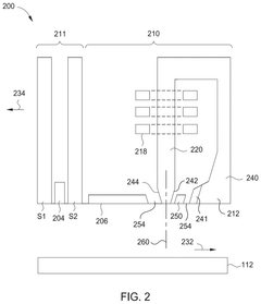
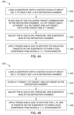
Improved YPtBi Composition in Spin Orbit Torque Devices
PatentPendingUS20250268110A1
Innovation
- A TSM layer comprising YPtBi with a 1:1.02:1.05 stoichiometry, which enhances the spin Hall angle and conductivity by adjusting the concentration ratios of Y, Pt, and Bi, and includes a buffer layer for optimal crystal orientation.
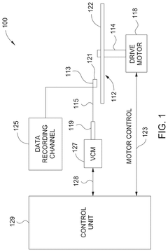
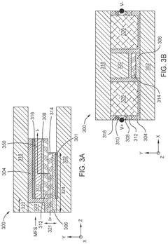
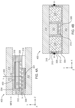
Spin-orbit torque SOT reader with recessed spin hall effect layer
PatentActiveUS12334123B2
Innovation
- A magnetic recording head design incorporating a SOT device with a recessed BiSb layer, where the BiSb layer is disposed over a free layer and recessed from the media facing surface (MFS), and shield notches are used to further recess the BiSb layer and reduce shield-to-shield spacing.
Material Characterization Techniques
Understanding the effect of grain structure on SOT (Spin-Orbit Torque) layer performance requires sophisticated material characterization techniques. Advanced microscopy methods, particularly Transmission Electron Microscopy (TEM) and Scanning Electron Microscopy (SEM), provide crucial insights into grain size, orientation, and boundary characteristics. These techniques enable researchers to visualize nanoscale features that significantly influence spin transport properties within SOT materials.
X-ray Diffraction (XRD) techniques, including grazing incidence XRD and pole figure analysis, offer quantitative data on crystallographic texture, lattice parameters, and phase composition. For SOT layers, where crystalline orientation can dramatically affect spin-orbit coupling strength, XRD provides essential structural information that correlates with device performance metrics.
Atomic Force Microscopy (AFM) and Magnetic Force Microscopy (MFM) enable surface topography mapping and magnetic domain visualization, respectively. These techniques are particularly valuable for understanding how grain structure affects interfacial roughness and local magnetic properties in SOT multilayer systems, where interface quality directly impacts spin current generation and transmission.
Spectroscopic techniques including X-ray Photoelectron Spectroscopy (XPS) and Auger Electron Spectroscopy (AES) provide elemental composition and chemical state information at grain boundaries and interfaces. These regions often contain impurities or oxidation that can significantly alter spin transport characteristics across the SOT layer structure.
Advanced synchrotron-based techniques such as X-ray Absorption Spectroscopy (XAS) and X-ray Magnetic Circular Dichroism (XMCD) offer element-specific magnetic information, critical for understanding how grain structure influences local magnetic moments and spin-orbit coupling in SOT materials.
Electrical transport measurements, including Hall effect measurements and magnetoresistance studies, complement structural characterization by directly probing how grain structure affects charge and spin transport. Four-point probe measurements across differently oriented grains can reveal anisotropic conductivity that impacts SOT efficiency.
Correlative characterization approaches, combining multiple techniques on identical sample regions, are increasingly important for establishing direct relationships between grain structure parameters and SOT performance metrics. For example, combining EBSD (Electron Backscatter Diffraction) with magnetotransport measurements allows researchers to correlate specific grain orientations with local SOT efficiency.
In-situ characterization methods enable observation of grain structure evolution during annealing or under applied fields, providing insights into stability and performance degradation mechanisms in SOT devices under operational conditions.
Manufacturing Scalability Assessment
The scalability of SOT (Spin-Orbit Torque) layer manufacturing processes represents a critical factor in determining the commercial viability of SOT-based magnetic memory technologies. Current manufacturing processes for SOT layers face significant challenges when transitioning from laboratory-scale production to high-volume manufacturing environments. The grain structure of SOT materials directly impacts performance consistency across wafers and between production batches, creating potential barriers to mass production.
Existing deposition techniques, including magnetron sputtering and atomic layer deposition (ALD), demonstrate varying degrees of scalability. Magnetron sputtering offers high throughput but struggles with precise control of grain boundaries and orientation at larger wafer sizes. Conversely, ALD provides excellent uniformity but at significantly reduced deposition rates, creating throughput limitations for high-volume manufacturing scenarios.
Equipment manufacturers have developed specialized tools to address these scalability challenges, with Applied Materials and Tokyo Electron introducing systems designed specifically for SOT layer deposition with improved grain structure control. These systems incorporate in-situ monitoring capabilities that allow real-time adjustment of deposition parameters to maintain consistent grain characteristics across 300mm wafers, representing a significant advancement in manufacturing capability.
Cost modeling analyses indicate that current SOT manufacturing processes remain approximately 30-40% more expensive than conventional MRAM production, primarily due to the additional process steps required to control grain structure. This cost differential presents a significant hurdle for widespread adoption, particularly in consumer electronics applications where price sensitivity is high.
Yield analysis from pilot production lines demonstrates that grain structure variability accounts for approximately 25% of device failures in SOT-based memory arrays. As production volumes increase, maintaining tight control over grain characteristics becomes exponentially more challenging, requiring more sophisticated process control methodologies and potentially specialized equipment.
Integration with existing semiconductor manufacturing flows presents another scalability consideration. The thermal budget requirements for optimal SOT grain formation may conflict with other process steps in a standard CMOS flow, necessitating careful process integration engineering. Several foundries have reported progress in developing modified process flows that accommodate these requirements without compromising overall device performance.
Looking forward, emerging deposition techniques such as high-power impulse magnetron sputtering (HiPIMS) and modified ALD processes show promise for improving the scalability of SOT layer manufacturing while maintaining the critical grain structure characteristics that enable optimal device performance. These techniques may provide the necessary balance between throughput, uniformity, and cost-effectiveness required for high-volume production environments.
Unlock deeper insights with Patsnap Eureka Quick Research — get a full tech report to explore trends and direct your research. Try now!
Generate Your Research Report Instantly with AI Agent
Supercharge your innovation with Patsnap Eureka AI Agent Platform!