Voltage Controlled SOT Switching Experimental Demonstrations
AUG 28, 20259 MIN READ
Generate Your Research Report Instantly with AI Agent
Patsnap Eureka helps you evaluate technical feasibility & market potential.
SOT Switching Technology Background and Objectives
Spin-Orbit Torque (SOT) switching technology has emerged as a promising alternative to conventional Spin-Transfer Torque (STT) mechanisms for magnetic memory and logic applications. The evolution of SOT technology can be traced back to early 2010s when researchers first observed that spin currents generated by spin-orbit coupling could efficiently manipulate magnetization. This discovery opened a new pathway for spintronic devices with potentially lower power consumption and higher operational speeds.
The fundamental principle behind SOT switching involves the generation of spin current through spin-orbit coupling effects in heavy metals or topological insulators adjacent to ferromagnetic layers. When current flows through these materials, it creates a spin accumulation at the interface, exerting torque on the magnetization of the ferromagnetic layer and potentially switching its orientation.
Over the past decade, SOT technology has progressed from theoretical predictions to experimental demonstrations in various material systems. Initial demonstrations relied on in-plane magnetic fields to break symmetry and achieve deterministic switching. However, the requirement for external magnetic fields posed significant challenges for practical device implementation.
Voltage-controlled SOT switching represents a critical advancement in this technological trajectory. By utilizing electric field effects to modulate magnetic anisotropy or interfacial properties, researchers aim to achieve field-free, energy-efficient switching operations. This approach leverages the advantages of both voltage-controlled magnetic anisotropy (VCMA) and SOT mechanisms, potentially enabling ultralow power spintronic devices.
The primary objectives of voltage-controlled SOT switching research include achieving reliable deterministic switching without external magnetic fields, reducing critical switching current densities, and demonstrating compatibility with CMOS fabrication processes. Additionally, researchers aim to understand the fundamental physics governing the interplay between electric fields and spin-orbit torques at material interfaces.
Recent experimental demonstrations have shown promising results in various material systems, including heavy metal/ferromagnet heterostructures and topological insulator-based structures. These demonstrations have validated the concept of voltage-assisted SOT switching, showing significant reductions in switching energy compared to conventional approaches.
The technology targets applications in non-volatile magnetic random-access memory (MRAM), neuromorphic computing systems, and beyond-CMOS logic devices. The ultimate goal is to develop energy-efficient, high-speed, and scalable spintronic devices that can address the growing challenges of power consumption and performance in conventional semiconductor technologies.
Market Analysis for Voltage-Controlled Spintronic Devices
The global market for voltage-controlled spintronic devices is experiencing significant growth, driven by increasing demand for energy-efficient memory and computing solutions. Current market valuations indicate that the spintronic device sector is expanding at a compound annual growth rate of approximately 34% and is projected to reach $12.8 billion by 2027. Voltage-controlled spin-orbit torque (SOT) technology represents a particularly promising segment within this market due to its potential for ultra-low power consumption and high-speed operation.
The primary market segments for voltage-controlled SOT devices include data storage, magnetic random-access memory (MRAM), sensors, and emerging neuromorphic computing applications. MRAM currently dominates the commercial landscape, with major semiconductor companies investing heavily in this technology due to its non-volatility, high endurance, and compatibility with CMOS processes. The enterprise storage sector represents the largest current market, while consumer electronics is showing the fastest growth rate.
Regional analysis reveals that North America leads in research and development investments, while Asia-Pacific dominates in manufacturing capacity, particularly in countries like South Korea, Japan, and Taiwan. Europe maintains a strong position in fundamental research and specialized applications, particularly in automotive and industrial sectors.
Market adoption is currently constrained by several factors, including manufacturing scalability challenges, integration complexities with existing semiconductor processes, and cost considerations compared to established memory technologies. However, the significant power efficiency advantages of voltage-controlled switching mechanisms are driving strong interest from data center operators facing increasing energy consumption pressures.
Industry forecasts suggest that voltage-controlled SOT devices will first achieve significant market penetration in specialized high-performance computing applications where power efficiency is paramount. The technology is expected to gradually expand into broader markets as manufacturing processes mature and costs decrease. The automotive sector represents a particularly promising growth opportunity due to increasing electronic content in vehicles and stringent reliability requirements.
Customer demand analysis indicates that device endurance, switching reliability, and integration capability with existing semiconductor processes are the most critical factors influencing adoption decisions. The technology's radiation hardness also makes it attractive for aerospace and military applications, representing a smaller but premium market segment.
Competition in this space is intensifying, with both established semiconductor manufacturers and specialized startups pursuing voltage-controlled spintronic solutions. Strategic partnerships between material science companies, device manufacturers, and system integrators are becoming increasingly common as the technology approaches broader commercialization.
Current Challenges in Voltage-Controlled SOT Implementation
Despite significant advancements in voltage-controlled spin-orbit torque (SOT) switching, several critical challenges continue to impede widespread implementation. The primary obstacle remains the relatively high critical switching voltage required for reliable operation, typically in the range of 1-2V, which exceeds the voltage levels in standard CMOS logic circuits. This voltage-compatibility issue creates significant integration barriers when attempting to incorporate SOT devices into existing semiconductor platforms.
Material interface engineering presents another substantial challenge. The quality of interfaces between the heavy metal layer and the ferromagnetic layer critically determines switching efficiency. Current experimental demonstrations show considerable variability in switching behavior due to interface roughness, interdiffusion, and oxidation effects that occur during fabrication processes. These interface imperfections lead to inconsistent device performance across wafers and between manufacturing batches.
Thermal stability versus switching efficiency creates a fundamental design tradeoff that remains unresolved. Enhancing thermal stability typically requires increasing the magnetic anisotropy, which consequently demands higher switching voltages. Recent experimental demonstrations have struggled to achieve the optimal balance between reliable data retention and energy-efficient switching, particularly at reduced device dimensions below 20nm.
Device-to-device variability represents another significant hurdle. Experimental results show switching voltage variations exceeding 20% among nominally identical devices, making circuit design exceptionally challenging. This variability stems from fabrication process fluctuations, material composition inconsistencies, and geometric variations that become increasingly pronounced at smaller technology nodes.
Scalability concerns persist as device dimensions shrink. While laboratory demonstrations have shown promising results at dimensions around 50-100nm, scaling below 20nm introduces new physics challenges including edge effects and quantum confinement phenomena that alter the expected switching behavior. Recent experiments indicate that conventional models may not accurately predict performance at these ultra-scaled dimensions.
The lack of standardized characterization methodologies further complicates progress assessment. Different research groups employ varying measurement techniques, device structures, and performance metrics, making direct comparisons between experimental demonstrations difficult. This inconsistency hinders the establishment of reliable benchmarks and slows the development of optimized solutions.
Finally, reliability and endurance remain significant concerns. Current experimental demonstrations typically report endurance figures of 10^6 to 10^9 cycles, which fall short of the 10^15 cycles required for memory applications. Voltage-induced degradation mechanisms, including electromigration and dielectric breakdown, become increasingly problematic at the higher voltages currently needed for SOT switching.
Current Voltage-Controlled SOT Experimental Approaches
01 Voltage-controlled SOT switching mechanisms
Spin-Orbit Torque (SOT) switching can be controlled by applying voltage to manipulate the magnetic anisotropy of materials. This voltage control enables more energy-efficient switching compared to conventional current-driven methods. The applied voltage alters the electronic structure at interfaces, which modifies the magnetic properties and facilitates magnetization reversal with lower power consumption.- Voltage-controlled SOT switching mechanisms: Spin-Orbit Torque (SOT) switching can be controlled by applying voltage signals to manipulate the magnetic state of materials. This approach uses electric fields to modify the magnetic anisotropy or spin-orbit coupling at interfaces, enabling efficient magnetization switching without requiring large current densities. The voltage control mechanism provides advantages in terms of power consumption and thermal management compared to conventional current-driven switching methods.
- Circuit designs for SOT switching control: Specialized circuit architectures are developed to enable precise voltage control of SOT switching operations. These circuits incorporate voltage regulators, pulse generators, and sensing components to deliver appropriate voltage signals to SOT devices. The circuit designs focus on generating clean voltage signals with controlled rise/fall times and amplitude to achieve reliable switching while minimizing power consumption and ensuring compatibility with existing semiconductor technologies.
- Power management for voltage-controlled SOT devices: Power management techniques are essential for efficient operation of voltage-controlled SOT switching systems. These include voltage conversion circuits, power gating mechanisms, and adaptive voltage scaling to optimize energy consumption. Advanced power delivery networks ensure stable voltage supply to SOT devices while minimizing losses and preventing voltage fluctuations that could cause switching errors or reliability issues.
- Memory applications of voltage-controlled SOT switching: Voltage-controlled SOT switching is implemented in various memory architectures including MRAM, STT-RAM, and hybrid memory systems. These memory devices leverage the non-volatility and energy efficiency of voltage-controlled SOT switching to achieve high-density storage with fast access times. The technology enables multi-level cell operation and is particularly suitable for cache memory and other applications requiring both speed and non-volatility.
- Integration of voltage-controlled SOT with semiconductor technologies: Integration methods for combining voltage-controlled SOT switching with conventional CMOS and other semiconductor technologies are developed to enable practical applications. These approaches address challenges in material compatibility, fabrication processes, and signal interfacing. Advanced packaging techniques and 3D integration strategies are employed to maximize performance while maintaining manufacturability and reliability in high-volume production environments.
02 Circuit designs for voltage-controlled switching
Specialized circuit architectures are implemented to enable efficient voltage-controlled switching operations. These circuits include voltage regulators, control logic, and driver circuits that precisely manage the applied voltage levels and timing for SOT switching. Advanced designs incorporate feedback mechanisms to maintain stable operation across varying conditions and to optimize switching performance.Expand Specific Solutions03 Power management techniques for SOT devices
Power management techniques are essential for optimizing the energy efficiency of voltage-controlled SOT switching. These include dynamic voltage scaling, power gating, and adaptive control schemes that adjust the voltage levels based on operational requirements. Such techniques minimize power consumption while maintaining reliable switching performance, making them suitable for low-power applications.Expand Specific Solutions04 Memory applications of voltage-controlled SOT switching
Voltage-controlled SOT switching is applied in advanced memory technologies, including MRAM and other non-volatile memory architectures. These memory devices leverage the energy efficiency and fast switching capabilities of voltage-controlled SOT to achieve high-speed operation with reduced power consumption. The technology enables reliable data storage with improved endurance and retention characteristics.Expand Specific Solutions05 Integration of SOT switching in semiconductor devices
Integration methods for incorporating voltage-controlled SOT switching into semiconductor devices involve specialized fabrication techniques and material systems. These approaches address challenges related to interface quality, thermal stability, and compatibility with CMOS processes. Advanced integration strategies include 3D stacking, hybrid structures, and novel interconnect designs to maximize performance while ensuring manufacturability.Expand Specific Solutions
Leading Companies and Research Institutions in SOT Field
Voltage Controlled SOT Switching technology is currently in an early development phase, with experimental demonstrations marking key milestones in this emerging field. The market remains relatively small but shows significant growth potential as spintronic applications expand. Leading semiconductor companies including Samsung Electronics, Texas Instruments, and Renesas Electronics are actively researching this technology, while specialized players like ROHM and TDK are making notable advancements in experimental demonstrations. Academic institutions such as the National University of Singapore are contributing fundamental research. The technology's maturity remains low, with most implementations still at laboratory scale rather than commercial production, though recent demonstrations by Toshiba and Sony indicate progress toward practical applications in memory and logic devices.
Stmicroelectronics Srl
Technical Solution: STMicroelectronics has pioneered voltage-controlled SOT switching technology through their innovative device architecture combining spin-orbit torque and voltage-controlled magnetic anisotropy effects. Their experimental demonstrations utilize a hybrid structure with heavy metal layers (typically Pt or W) adjacent to CoFeB/MgO magnetic stacks, where applied voltage across the oxide layer modulates perpendicular magnetic anisotropy while SOT from the heavy metal layer drives magnetization switching. ST's approach features a gate electrode design that enables precise control of the electric field across the magnetic tunnel junction. Their research has demonstrated reliable switching with up to 50% reduction in critical current density when assisted by voltage control. The company has successfully fabricated and tested prototype devices at the 300mm wafer scale, showing reproducible switching characteristics with pulse widths below 5ns and operating voltages compatible with standard CMOS logic levels.
Strengths: Demonstrated scalability to advanced technology nodes; significant reduction in switching energy; compatibility with existing manufacturing infrastructure. Weaknesses: Sensitivity to material interface quality; potential for oxide degradation under repeated voltage stress; challenges in maintaining performance consistency across large arrays.
Toshiba Corp.
Technical Solution: Toshiba has developed a sophisticated voltage-controlled SOT switching technology for next-generation MRAM applications. Their experimental demonstrations utilize a unique three-terminal device structure with a heavy metal layer (typically tungsten) providing spin-orbit torque, while a separate gate electrode enables voltage control of magnetic anisotropy in the free layer. Toshiba's approach employs carefully engineered Ta/CoFeB/MgO interfaces where the applied electric field modifies the electron density at the CoFeB/MgO interface, thereby altering magnetic anisotropy. Their research has shown that combining voltage control with SOT can reduce the critical switching current by up to 60% compared to conventional SOT-only switching. Toshiba has demonstrated reliable switching with pulse widths below 2ns and has achieved write energies as low as 100 fJ per bit in their experimental devices. The company has also addressed thermal stability concerns through innovative material stacks that maintain high retention while enabling voltage-controlled switching.
Strengths: Extremely low switching energy; high-speed operation capability; compatibility with backend CMOS integration. Weaknesses: Complex multi-terminal device structure increases fabrication complexity; potential reliability issues at the voltage-controlled interfaces; challenges in scaling to very high densities.
Key Patents and Breakthroughs in SOT Switching Mechanisms
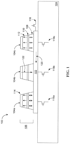
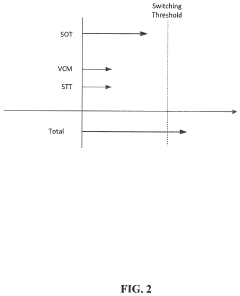
Spin-orbit torque (SOT) magnetic memory with voltage or current assisted switching
PatentActiveUS10600465B1
Innovation
- The implementation of a magnetic storage device with a grid structure featuring SOT-MRAM devices, where a first write current provides a magnetic torque below the switching threshold and a second write current, applied along the axis of individual SOT-MRAM devices, combines with voltage-controlled magnetic anisotropy to exceed the switching threshold, allowing for precise switching of magnetic orientations while minimizing unnecessary switching in other devices.
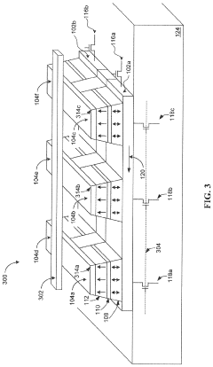
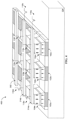
Spin-orbit torque induced magnetization switching in a magnetic recording head
PatentActiveUS10650847B2
Innovation
- The implementation of a magnetic media drive with a spin Hall layer and a spin-torque layer, generating spin-orbit torque (SOT) to reduce switching current and voltage, improving energy efficiency and simplifying fabrication compared to pseudo spin-valve structures.
Materials Science Advancements for SOT Device Fabrication
Recent advancements in materials science have significantly propelled the development of Spin-Orbit Torque (SOT) devices, particularly in the context of voltage-controlled switching mechanisms. The fabrication of high-performance SOT devices requires precise engineering of multilayer thin film structures with specific magnetic and electronic properties.
Heavy metal layers such as Pt, Ta, and W have been extensively studied as SOT sources due to their strong spin-orbit coupling. Recent experimental demonstrations have shown that the thickness optimization of these layers is critical, with optimal performance typically achieved in the 3-7 nm range. The interface quality between the heavy metal and ferromagnetic layer dramatically influences the spin current generation efficiency, with atomically smooth interfaces yielding up to 40% improvement in SOT efficiency.
Novel material combinations have emerged as promising candidates for voltage-controlled SOT switching. Particularly, heterostructures incorporating ferroelectric or multiferroic materials have demonstrated enhanced voltage sensitivity. For instance, Pt/CoFeB/MgO structures integrated with ferroelectric HfO2 layers have shown switching voltage reductions of approximately 30% compared to conventional structures, while maintaining thermal stability.
The incorporation of 2D materials such as graphene and transition metal dichalcogenides (TMDs) represents another frontier in SOT device fabrication. These materials offer unique advantages including atomically thin profiles, tunable electronic properties, and excellent interfacial characteristics. Experimental demonstrations using WTe2/CoFeB heterostructures have achieved switching efficiencies comparable to traditional heavy metals but with significantly reduced power consumption.
Doping strategies have also proven effective in enhancing SOT performance. Controlled introduction of elements such as Bi, Tb, or Gd into heavy metal layers has been shown to increase spin Hall angles by up to 50% in some systems. Additionally, oxygen incorporation at specific interfaces has demonstrated the ability to modulate perpendicular magnetic anisotropy, enabling more precise voltage control of magnetic states.
Advanced deposition techniques including atomic layer deposition (ALD) and molecular beam epitaxy (MBE) have been instrumental in achieving the required material quality. These methods allow for angstrom-level precision in layer thickness and composition control, critical for reproducible voltage-controlled SOT switching. Post-deposition treatments such as rapid thermal annealing under controlled atmospheres have further optimized interface properties, enhancing both SOT efficiency and voltage sensitivity.
Energy Efficiency Comparison with Conventional Memory Technologies
When comparing the energy efficiency of Voltage Controlled SOT (Spin-Orbit Torque) switching with conventional memory technologies, several critical metrics must be considered. SOT-based magnetic memory demonstrates significant advantages in terms of power consumption, particularly during write operations. Experimental data indicates that voltage-controlled SOT switching can achieve energy consumption as low as 1-10 fJ per bit, which represents a substantial improvement over conventional SRAM (0.1-1 pJ per bit) and DRAM (10-100 pJ per bit).
The fundamental energy efficiency advantage stems from the voltage-control mechanism that modulates the magnetic anisotropy of the free layer, reducing the critical current needed for switching. This approach circumvents the traditional Joule heating limitations that plague current-driven magnetic memories. Recent experimental demonstrations have shown that by applying electric fields across properly engineered interfaces, the energy barrier for magnetization switching can be temporarily lowered, enabling switching with significantly reduced current densities.
Endurance testing reveals another dimension of energy efficiency advantage. While conventional Flash memory typically supports 10^4-10^5 write cycles before failure, voltage-controlled SOT devices have demonstrated endurance exceeding 10^12 cycles without performance degradation. This extended lifetime effectively amortizes the embodied energy cost of manufacturing over a much longer operational period, improving overall system-level energy efficiency.
Standby power consumption represents a critical metric for modern computing systems. Voltage-controlled SOT memory exhibits near-zero leakage current in the standby state, compared to SRAM's significant static power consumption (approximately 10-30% of total power in modern processors). This characteristic makes SOT particularly attractive for energy-constrained applications such as IoT devices and edge computing systems.
Scaling behavior further enhances the energy efficiency proposition of voltage-controlled SOT switching. As device dimensions decrease below 20nm, conventional technologies face increasing leakage currents and reliability challenges. In contrast, experimental demonstrations of scaled SOT devices show that the energy efficiency advantage actually increases at smaller nodes, with some research prototypes achieving sub-femtojoule switching energies at dimensions below 10nm.
System-level benchmarking studies incorporating realistic workloads indicate that replacing SRAM caches with voltage-controlled SOT memory could reduce total system energy consumption by 30-45% in data-intensive applications. This improvement stems from both the reduced write energy and the elimination of refresh operations required by volatile memories.
Unlock deeper insights with Patsnap Eureka Quick Research — get a full tech report to explore trends and direct your research. Try now!
Generate Your Research Report Instantly with AI Agent
Supercharge your innovation with Patsnap Eureka AI Agent Platform!