Noise And Variability Analysis In SOT MRAM Arrays
AUG 28, 20259 MIN READ
Generate Your Research Report Instantly with AI Agent
Patsnap Eureka helps you evaluate technical feasibility & market potential.
SOT MRAM Technology Background and Objectives
Spin-Orbit Torque Magnetoresistive Random Access Memory (SOT-MRAM) represents a significant advancement in non-volatile memory technology, emerging from decades of research in spintronics and magnetic materials. The evolution of MRAM technology began with Toggle MRAM in the early 2000s, progressed through Spin-Transfer Torque (STT) MRAM, and has now reached the SOT-MRAM paradigm, which offers superior performance characteristics including enhanced endurance, faster switching speeds, and reduced write energy.
The fundamental operating principle of SOT-MRAM relies on the manipulation of magnetic states through spin-orbit coupling effects, particularly the spin Hall effect and Rashba effect. These quantum mechanical phenomena enable the conversion of charge current into spin current, which can efficiently switch the magnetization direction of the free layer in magnetic tunnel junctions (MTJs) without passing current through the tunnel barrier.
Current technological trends indicate a growing interest in SOT-MRAM for applications requiring high-speed cache memory, as it potentially offers write speeds comparable to SRAM while maintaining the non-volatility advantage. Industry projections suggest that SOT-MRAM could achieve write speeds below 1ns with appropriate materials engineering and device optimization, positioning it as a viable candidate for universal memory applications.
The primary technical objectives for SOT-MRAM development focus on addressing several critical challenges. First, enhancing the spin-orbit torque efficiency to reduce switching current densities, which currently range from 10^7 to 10^8 A/cm². Second, improving thermal stability to ensure reliable data retention at reduced dimensions. Third, developing manufacturing processes compatible with existing CMOS technology for seamless integration into semiconductor fabrication flows.
Noise and variability analysis in SOT-MRAM arrays represents a crucial research direction, as device-to-device variations significantly impact yield and reliability in high-density memory applications. These variations stem from multiple sources including process-induced geometric fluctuations, material composition inconsistencies, and intrinsic stochastic effects during magnetization switching.
The investigation of noise mechanisms in SOT-MRAM encompasses thermal noise, shot noise, 1/f noise, and random telegraph noise (RTN), all of which can affect read and write operations. Understanding these noise sources is essential for developing robust error correction schemes and reliability models for commercial deployment.
This technical exploration aims to comprehensively characterize noise and variability phenomena in SOT-MRAM arrays, establish their physical origins, quantify their impact on device performance, and propose mitigation strategies. The ultimate goal is to enable the scaling of SOT-MRAM technology to sub-20nm dimensions while maintaining acceptable bit error rates and performance consistency across large arrays.
Market Analysis for SOT MRAM Applications
The SOT-MRAM (Spin-Orbit Torque Magnetic Random Access Memory) market is experiencing significant growth potential as industries seek more efficient, non-volatile memory solutions. Current market projections indicate that the overall MRAM market will reach approximately $5 billion by 2028, with SOT-MRAM expected to capture an increasing share as the technology matures. This growth is primarily driven by the inherent advantages of SOT-MRAM, including lower power consumption, improved endurance, and faster switching speeds compared to conventional STT-MRAM technologies.
The automotive sector represents one of the most promising application areas for SOT-MRAM, particularly in advanced driver-assistance systems (ADAS) and autonomous vehicles. These applications require memory solutions that can withstand extreme temperatures and offer radiation hardness while maintaining data integrity. The automotive memory market alone is projected to grow at a CAGR of 18% through 2026, creating substantial opportunities for SOT-MRAM implementation.
Data centers and enterprise storage systems constitute another significant market segment for SOT-MRAM adoption. With the exponential growth in data processing requirements and the push for energy efficiency, SOT-MRAM's combination of non-volatility and SRAM-like performance positions it as an attractive solution for cache memory and storage class memory applications. Industry analysts estimate that data center memory solutions could represent 30% of the total MRAM market by 2025.
The Internet of Things (IoT) ecosystem presents a diverse range of applications for SOT-MRAM. Edge computing devices require memory solutions that balance performance with energy efficiency, making SOT-MRAM particularly suitable. The edge AI chipset market is growing at 21% annually, with memory components being critical to overall system performance and power consumption profiles.
Consumer electronics manufacturers are increasingly exploring SOT-MRAM for next-generation smartphones, wearables, and portable devices. The ability to reduce standby power consumption while maintaining fast access times addresses key pain points in mobile device design. Market penetration in this sector remains limited but is expected to accelerate as manufacturing processes mature and costs decrease.
Industrial applications, including factory automation, industrial IoT, and smart grid technologies, represent another growth vector for SOT-MRAM. These environments often require memory solutions that can operate reliably under harsh conditions while maintaining data integrity during power interruptions. The industrial memory market segment is projected to grow steadily at 15% annually through 2027.
Despite these promising market opportunities, challenges remain in scaling SOT-MRAM production to meet competitive price points. Current manufacturing costs exceed those of established memory technologies, limiting widespread adoption. However, as production volumes increase and fabrication processes improve, the cost gap is expected to narrow significantly over the next 3-5 years.
Current Challenges in SOT MRAM Noise Characterization
The characterization and analysis of noise in Spin-Orbit Torque Magnetic Random Access Memory (SOT-MRAM) arrays present significant technical challenges that impede both research advancement and commercial deployment. At the device level, thermal fluctuations introduce stochastic behavior in magnetization switching, creating read/write reliability issues that are difficult to predict and control. These thermal effects become more pronounced as device dimensions shrink below 20nm, where the thermal stability factor decreases substantially.
Signal-to-noise ratio (SNR) degradation represents another critical challenge, particularly during the read operation. The tunnel magnetoresistance (TMR) signal can be overwhelmed by various noise sources including 1/f noise, random telegraph noise (RTN), and shot noise. Current measurement techniques struggle to isolate and quantify these different noise contributions, especially when they occur simultaneously or exhibit temporal variations.
Process-induced variability further complicates noise characterization. Manufacturing inconsistencies lead to device-to-device variations in critical parameters such as magnetic anisotropy, damping constant, and SOT efficiency. These variations manifest as statistical distributions of switching currents and read signals across arrays, making standardized noise models inadequate for accurate yield prediction.
The measurement infrastructure itself introduces additional challenges. Conventional noise measurement setups often lack the bandwidth and sensitivity required for nanosecond-scale switching events characteristic of SOT-MRAM. Furthermore, the electrical probing of individual cells within dense arrays can introduce parasitic effects that contaminate the intrinsic noise signature of the device.
Temperature dependence of noise characteristics presents yet another layer of complexity. SOT-MRAM devices exhibit different noise profiles across their operating temperature range (-40°C to 125°C for automotive applications), but comprehensive temperature-dependent noise models remain underdeveloped. This gap is particularly problematic for applications requiring operation in extreme environments.
Array-level effects, including cross-talk between adjacent cells and power supply fluctuations, create correlated noise patterns that cannot be characterized through single-cell measurements. These system-level noise sources can trigger unexpected write errors or read disturbances that compromise data integrity across the entire memory array.
Finally, there exists a fundamental challenge in establishing standardized noise metrics and measurement protocols for SOT-MRAM. The lack of industry consensus on noise characterization methodologies hampers meaningful comparison between different device architectures and fabrication approaches, ultimately slowing the optimization process and technology maturation.
Existing Noise Mitigation Techniques for SOT MRAM Arrays
01 Noise reduction techniques in SOT MRAM arrays
Various techniques can be employed to reduce noise in Spin-Orbit Torque Magnetic Random Access Memory (SOT MRAM) arrays. These include optimizing the materials used in the magnetic tunnel junction (MTJ), implementing specialized circuit designs to filter out noise, and using advanced signal processing algorithms. By reducing noise, the reliability and performance of SOT MRAM arrays can be significantly improved, leading to more stable read and write operations.- Noise reduction techniques in SOT MRAM arrays: Various techniques can be employed to reduce noise in Spin-Orbit Torque Magnetic Random Access Memory (SOT MRAM) arrays. These include optimizing the materials used in the magnetic tunnel junction (MTJ), implementing specialized circuit designs to filter out noise, and using advanced signal processing algorithms. By reducing noise, the reliability and performance of SOT MRAM arrays can be significantly improved, leading to more stable read and write operations.
- Variability management in SOT MRAM fabrication: Managing variability in the fabrication process of SOT MRAM arrays is crucial for ensuring consistent performance across devices. This includes controlling process parameters during deposition of magnetic layers, optimizing annealing conditions, and implementing statistical process control methods. Techniques such as adaptive programming algorithms and reference cell designs can also help compensate for device-to-device variations, improving the overall yield and reliability of SOT MRAM arrays.
- Array architecture for minimizing noise and variability: Specialized array architectures can be designed to minimize the impact of noise and variability in SOT MRAM. These architectures may include differential sensing schemes, hierarchical bit-line structures, and optimized word-line configurations. By carefully designing the array layout and implementing appropriate isolation techniques, cross-talk between adjacent cells can be reduced, leading to improved signal-to-noise ratio and more reliable operation of the memory array.
- Sensing circuits for improved noise immunity: Advanced sensing circuits play a critical role in mitigating the effects of noise and variability in SOT MRAM arrays. These circuits may incorporate techniques such as time-domain sensing, offset cancellation, and dynamic reference generation. By implementing sophisticated sensing schemes with high noise immunity, the read margin can be improved, allowing for reliable detection of the stored data even in the presence of device variations and environmental noise.
- Thermal stability and environmental effects on SOT MRAM performance: Thermal effects and environmental conditions can significantly impact the noise and variability characteristics of SOT MRAM arrays. Techniques to enhance thermal stability include optimizing the magnetic anisotropy of the free layer, implementing heat-resistant materials, and designing temperature-compensated reference schemes. Additionally, shielding methods and specialized packaging can help protect the arrays from external magnetic fields and other environmental factors that could introduce noise or variability in device performance.
02 Variability management in SOT MRAM fabrication
Managing variability during the fabrication process of SOT MRAM arrays is crucial for ensuring consistent performance. This includes controlling process parameters such as film thickness, composition, and annealing conditions. Advanced lithography techniques and precise deposition methods can help minimize device-to-device variations. Post-fabrication calibration and compensation techniques can also be implemented to address remaining variability issues in the manufactured arrays.Expand Specific Solutions03 Thermal stability enhancement for SOT MRAM
Thermal stability is a critical factor affecting the noise and variability in SOT MRAM arrays. Various approaches can be used to enhance thermal stability, including the development of materials with higher magnetic anisotropy, optimized layer structures, and thermal management techniques. By improving thermal stability, the retention time of stored data can be increased, and the susceptibility to thermal noise can be reduced, resulting in more reliable memory operation.Expand Specific Solutions04 Circuit design strategies for SOT MRAM arrays
Specialized circuit designs can significantly mitigate noise and variability issues in SOT MRAM arrays. These include sense amplifiers with high noise immunity, reference schemes that compensate for process variations, and write drivers that provide consistent current pulses. Advanced error correction codes and redundancy schemes can also be implemented at the circuit level to improve the overall reliability of SOT MRAM arrays despite inherent device variations.Expand Specific Solutions05 Testing and characterization methods for SOT MRAM variability
Comprehensive testing and characterization methods are essential for understanding and addressing noise and variability in SOT MRAM arrays. These include statistical analysis of device parameters, noise spectrum measurements, and accelerated reliability testing. Advanced characterization techniques such as magnetic force microscopy and time-resolved measurements can provide insights into the physical mechanisms underlying variability. These methods enable the development of more robust SOT MRAM technologies with improved performance consistency.Expand Specific Solutions
Leading Companies and Research Institutions in SOT MRAM
The SOT MRAM arrays technology landscape is currently in a transitional phase from early development to commercial adoption, with the market expected to grow significantly as demand for energy-efficient, non-volatile memory solutions increases. The competitive field is dominated by major semiconductor manufacturers including TSMC, Samsung, Intel, and IBM, who are investing heavily in R&D to address noise and variability challenges in SOT MRAM arrays. These companies are at different stages of technical maturity, with some focusing on fundamental research while others are progressing toward production-ready solutions. Specialized players like Antaios are emerging with innovative approaches, while research institutions such as CNRS and various universities are contributing critical advancements in understanding and mitigating noise factors. The technology is approaching commercial viability but still requires significant optimization for widespread adoption.
International Business Machines Corp.
Technical Solution: IBM has developed comprehensive noise and variability analysis methodologies specifically for SOT-MRAM arrays. Their approach combines device-level characterization with array-level testing to identify and mitigate various noise sources. IBM's technical solution includes advanced statistical modeling techniques that account for process variations, thermal fluctuations, and read/write disturbances in SOT-MRAM cells. They've implemented specialized test structures within their arrays to isolate different noise components, allowing for precise characterization of read noise, write variability, and retention failures. IBM has also developed proprietary circuit techniques to compensate for device-to-device variations, including adaptive sensing schemes and reference cell calibration methods that dynamically adjust to changing environmental conditions and aging effects. Their solution incorporates machine learning algorithms to predict and compensate for variability patterns across large arrays, significantly improving yield and reliability metrics.
Strengths: IBM's approach benefits from their extensive experience in memory technologies and manufacturing processes, allowing for highly accurate noise modeling. Their solutions effectively address both systematic and random variations in SOT-MRAM arrays. Weaknesses: The complexity of their analysis methods requires sophisticated testing equipment and may increase development costs. Some of their compensation techniques introduce additional circuit overhead that can impact array density.
Samsung Electronics Co., Ltd.
Technical Solution: Samsung has pioneered a multi-tiered approach to noise and variability analysis in SOT-MRAM arrays. Their solution incorporates both physical and electrical characterization techniques to comprehensively evaluate noise sources at different levels of integration. At the device level, Samsung employs high-precision measurement systems to characterize intrinsic fluctuations in magnetic tunnel junctions, including thermal noise, shot noise, and 1/f noise components. For array-level analysis, they've developed specialized test chips with embedded sensors that can monitor local variations in temperature, supply voltage, and magnetic field strength - all critical factors affecting SOT-MRAM performance. Samsung's methodology includes statistical process control techniques that track key parameters across wafers and lots to identify systematic variation patterns. Their solution also features adaptive circuit techniques that can compensate for device-to-device variations, including programmable reference cells and dynamic sensing schemes that adjust thresholds based on measured noise levels. Samsung has implemented these techniques in their latest SOT-MRAM test arrays, demonstrating significant improvements in read margin and write reliability.
Strengths: Samsung's comprehensive approach addresses noise sources across multiple integration levels, from individual devices to full arrays. Their solution benefits from the company's extensive manufacturing expertise, allowing for practical implementation in high-volume production. Weaknesses: The solution requires significant overhead in terms of test structures and monitoring circuits, potentially reducing effective array density. Some compensation techniques may increase power consumption during read/write operations.
Critical Patents and Literature on SOT MRAM Variability
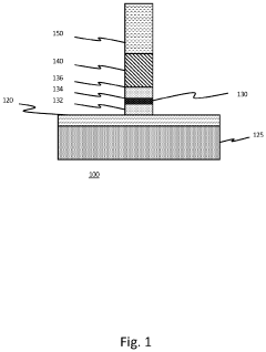
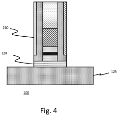
Spin-orbit torque magnetoresistive random access memory array
PatentPendingJP2024528302A
Innovation
- Integration of SOT-MRAM cell stack with a diode structure in each unit cell, enabling more efficient array organization and potentially reducing cross-talk between cells.
- Novel array architecture where one column includes a source line contacting source contacts of each transistor, while SOT lines contact drain contacts of transistors in each row, optimizing the cell access scheme.
- Vertical integration approach with the SOT-MRAM cell stack positioned above the SOT line and connected to it, maximizing density while maintaining electrical performance.
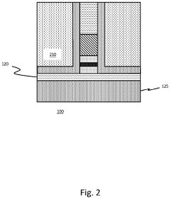
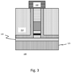
Spin-orbit-torque magnetoresistive random-access memory array
PatentActiveUS12020736B2
Innovation
- Incorporating a diode structure above the SOT-MRAM cell stack and using a single transistor for both read and write operations, with a cylindrical diode enabling control of current flow through a single transistor, reducing pattern complexity and increasing die density.
Manufacturing Process Optimization for SOT MRAM Yield
The optimization of manufacturing processes for SOT MRAM yield represents a critical challenge in the commercialization pathway of this emerging memory technology. Current fabrication techniques for Spin-Orbit Torque Magnetic Random Access Memory arrays exhibit significant variability issues that directly impact device performance and reliability. Process optimization must address multiple interconnected factors across the manufacturing chain.
Material deposition techniques require particular attention, as the quality and uniformity of magnetic layers significantly influence device characteristics. Sputtering parameters, including pressure, power, and target composition, must be precisely controlled to ensure consistent magnetic properties across the wafer. Advanced techniques such as atomic layer deposition (ALD) show promise for achieving better uniformity in critical layers, though implementation challenges remain regarding throughput and cost-effectiveness.
Lithography optimization presents another crucial aspect, with feature size reduction demanding enhanced resolution and alignment precision. Extreme ultraviolet lithography (EUV) offers potential advantages for SOT MRAM fabrication, enabling more precise patterning of nanoscale elements while reducing edge roughness that contributes to device-to-device variability. However, EUV implementation requires significant capital investment and process development.
Etching processes substantially impact device performance through their effect on sidewall profiles and potential damage to magnetic layers. Reactive ion etching parameters must be carefully tuned to minimize magnetic property degradation while maintaining dimensional control. Ion beam etching with precise angle control shows promise for reducing variability in critical magnetic stack structures.
Post-deposition annealing represents a critical step for crystallization and interface quality enhancement. Temperature ramping profiles and magnetic field application during annealing significantly influence magnetic layer properties. Statistical process control methods have demonstrated effectiveness in optimizing these parameters for reduced variability.
Integration of in-line metrology and advanced process control systems enables real-time monitoring and adjustment of critical parameters. Techniques such as magneto-optical Kerr effect measurements and four-point probe testing provide valuable feedback for process optimization. Machine learning algorithms are increasingly being deployed to identify complex parameter interactions that affect yield.
Contamination control protocols require enhancement beyond standard CMOS processes due to the sensitivity of magnetic materials to impurities. Dedicated equipment and specialized cleaning procedures have shown effectiveness in reducing defect-related variability in SOT MRAM arrays, though implementation costs remain a consideration for manufacturing scale-up.
Reliability Testing Methodologies for SOT MRAM Arrays
Reliability testing methodologies for SOT-MRAM arrays must address the unique noise and variability challenges inherent in this emerging memory technology. Comprehensive testing frameworks typically begin with device-level characterization, where individual memory cells undergo rigorous electrical parameter extraction to establish baseline performance metrics. These parameters include switching current thresholds, read/write margins, and thermal stability factors that directly impact reliability under various operating conditions.
Statistical analysis forms the cornerstone of SOT-MRAM reliability assessment, requiring large sample sizes to accurately capture the distribution of performance parameters across arrays. Advanced statistical methods such as Weibull analysis and extreme value statistics help identify potential failure modes and predict long-term reliability behavior. These approaches enable quantification of both systematic and random variations that affect memory performance.
Accelerated life testing protocols have been specifically adapted for SOT-MRAM technology to simulate years of operation within compressed timeframes. These protocols typically involve elevated temperatures, increased operating voltages, and higher switching frequencies to stress the devices beyond normal operating conditions. The resulting data allows for extrapolation of failure rates and determination of mean time to failure (MTTF) metrics that are critical for commercial viability assessment.
Environmental stress testing represents another crucial dimension of SOT-MRAM reliability evaluation. Arrays must be subjected to temperature cycling (-40°C to 125°C), humidity exposure, and electromagnetic interference to verify robustness across diverse deployment scenarios. Recent methodologies have incorporated radiation testing to assess soft error rates, particularly important for aerospace and military applications where radiation-induced failures present significant concerns.
Endurance testing methodologies focus on write cycle limitations, with current protocols requiring demonstration of at least 10^12 write cycles for competitive positioning against existing memory technologies. Advanced test equipment employing high-speed pulse generators and precision measurement systems enables efficient execution of these extensive cycling tests while monitoring performance degradation indicators such as resistance drift and switching current variations.
Read disturb immunity testing has emerged as a critical reliability metric specific to SOT-MRAM arrays. This methodology evaluates the probability of unintended state changes during repeated read operations, which can occur due to the partial activation of switching mechanisms by read currents. Sophisticated bit error rate testers (BERTs) are typically employed to quantify these effects at both cell and array levels.
Unlock deeper insights with Patsnap Eureka Quick Research — get a full tech report to explore trends and direct your research. Try now!
Generate Your Research Report Instantly with AI Agent
Supercharge your innovation with Patsnap Eureka AI Agent Platform!