

SOT MRAM Product Roadmap For Embedded Non Volatile Cache
AUG 28, 20259 MIN READ
Generate Your Research Report Instantly with AI Agent
PatSnap Eureka helps you evaluate technical feasibility & market potential.
SOT MRAM Evolution and Development Objectives
Spin-Orbit Torque Magnetic Random Access Memory (SOT-MRAM) represents a significant evolution in non-volatile memory technology, emerging from earlier MRAM variants to address critical limitations in speed, endurance, and power consumption. The development of SOT-MRAM began in the early 2010s, building upon the foundation established by Spin-Transfer Torque MRAM (STT-MRAM) but introducing a fundamental innovation in the switching mechanism that separates the read and write paths.
The technological trajectory of SOT-MRAM has been characterized by progressive improvements in materials science, particularly in the development of heavy metal layers that enhance the spin-orbit coupling effect. Early research focused primarily on proof-of-concept demonstrations, while recent advancements have shifted toward optimizing device parameters for commercial viability, especially for embedded cache applications where both non-volatility and high performance are required.
Current industry trends indicate an accelerating interest in SOT-MRAM as a potential replacement for SRAM and embedded flash in advanced semiconductor nodes below 28nm. This interest is driven by SRAM's increasing leakage current issues and embedded flash's scaling limitations, creating a technological gap that SOT-MRAM is uniquely positioned to fill.
The primary technical objectives for SOT-MRAM development in embedded non-volatile cache applications include achieving write speeds comparable to SRAM (<10ns), reducing switching current density while maintaining thermal stability, enhancing endurance beyond 10^16 cycles, and ensuring compatibility with standard CMOS manufacturing processes. These objectives align with the industry's need for memory solutions that combine the speed of volatile memory with the persistence of non-volatile storage.
Material innovation represents a critical aspect of the SOT-MRAM roadmap, with research focusing on novel heavy metal/ferromagnet interfaces that maximize spin-orbit coupling efficiency. Concurrently, device architecture optimization aims to reduce cell size while maintaining performance, with a target of achieving competitive bit density compared to SRAM at advanced nodes.
Integration challenges form another key development objective, particularly addressing the thermal budget constraints of back-end-of-line processing and ensuring reliable electrical connections between the SOT-MRAM array and peripheral CMOS circuitry. The roadmap also emphasizes the importance of developing sophisticated sensing schemes to accommodate the relatively low magnetoresistance ratio of SOT-MRAM cells.
Looking forward, the SOT-MRAM evolution trajectory aims toward demonstration of fully functional cache hierarchies by 2025, with initial commercial deployment in specialized high-reliability applications, followed by broader adoption in mainstream computing platforms as the technology matures and manufacturing costs decrease.
Market Analysis for Embedded Non-Volatile Cache Solutions
The embedded non-volatile cache solutions market is experiencing significant growth driven by the increasing demand for high-performance computing systems across various industries. The global market for embedded non-volatile memory solutions was valued at approximately $2.1 billion in 2022 and is projected to reach $4.5 billion by 2028, representing a compound annual growth rate (CAGR) of 13.5%. This growth trajectory is primarily fueled by the expanding applications in automotive electronics, industrial automation, Internet of Things (IoT) devices, and advanced computing systems.
SOT-MRAM (Spin-Orbit Torque Magnetic Random Access Memory) technology is emerging as a promising solution for embedded non-volatile cache applications, competing with established technologies such as embedded Flash, SRAM with battery backup, and other emerging non-volatile memory technologies like RRAM and PCM. The market demand for SOT-MRAM is particularly strong in sectors requiring high-speed, low-power, and reliable memory solutions with non-volatility features.
The automotive sector represents one of the largest market segments for embedded non-volatile cache solutions, accounting for approximately 28% of the total market share. The increasing integration of advanced driver-assistance systems (ADAS) and autonomous driving capabilities necessitates robust memory solutions that can maintain data integrity under extreme conditions while delivering high performance.
Enterprise computing and data centers constitute another significant market segment, representing about 24% of the total market. The growing adoption of edge computing architectures and the need for energy-efficient data processing solutions are driving the demand for advanced non-volatile cache technologies like SOT-MRAM.
Consumer electronics, including smartphones, tablets, and wearable devices, accounts for roughly 22% of the market. These applications benefit from SOT-MRAM's combination of speed, endurance, and non-volatility, enabling enhanced user experiences and extended battery life.
Industrial applications, including factory automation, smart manufacturing, and industrial IoT, represent approximately 18% of the market. These environments often require memory solutions that can operate reliably in harsh conditions and maintain data integrity during power interruptions.
Market analysis indicates that the Asia-Pacific region dominates the embedded non-volatile cache market with a 45% share, followed by North America (30%) and Europe (20%). This regional distribution reflects the concentration of semiconductor manufacturing facilities and electronic device production in these areas.
Customer requirements for embedded non-volatile cache solutions are increasingly focused on higher density, lower power consumption, improved reliability, and enhanced security features. SOT-MRAM's ability to address these requirements positions it favorably against competing technologies, particularly as manufacturing processes mature and production costs decrease.
SOT MRAM Technical Challenges and Global Development Status
SOT-MRAM (Spin-Orbit Torque Magnetic Random Access Memory) technology has emerged as a promising candidate for embedded non-volatile cache applications, offering significant advantages over conventional memory technologies. However, several technical challenges must be addressed before widespread commercial adoption can occur.
The primary technical challenge facing SOT-MRAM development is achieving the optimal balance between thermal stability and switching current density. Current SOT-MRAM designs struggle to maintain data retention at reduced dimensions while simultaneously requiring reasonable switching currents. This fundamental trade-off represents a significant barrier to scaling and energy efficiency.
Material engineering challenges also persist in SOT-MRAM development. The heavy metal layer, which generates the spin current through spin-orbit coupling, requires careful optimization of thickness, composition, and interface quality. Additionally, the magnetic free layer must be engineered to achieve perpendicular magnetic anisotropy with sufficient thermal stability while remaining responsive to spin torque.
Device integration presents another substantial hurdle. Incorporating SOT-MRAM into standard CMOS processes requires addressing issues related to material compatibility, thermal budgets, and etching processes. The three-terminal design of SOT-MRAM, while offering advantages in terms of read/write decoupling, introduces layout complexity that impacts cell size and integration density.
Globally, SOT-MRAM research and development efforts are concentrated in several key regions. The United States leads in fundamental research through institutions like Stanford University and companies such as Intel and IBM. Europe has established strong research clusters, particularly in France through Spintec and Germany through Infineon Technologies. In Asia, South Korea (Samsung, SK Hynix) and Japan (Toshiba, Sony) have made significant investments in SOT-MRAM technology.
Recent technological breakthroughs have accelerated SOT-MRAM development. These include the demonstration of sub-nanosecond switching speeds, reduction in critical switching current densities through novel material stacks, and improved thermal stability through synthetic antiferromagnetic structures. However, reliability issues such as read disturbance, write error rates, and endurance limitations continue to challenge researchers.
The development status varies significantly across different applications. For embedded cache applications, SOT-MRAM is approaching technology readiness levels suitable for initial product integration, with several companies reporting successful test chips. However, for standalone memory applications, significant challenges remain in achieving competitive density and cost metrics compared to established technologies.
Current SOT MRAM Implementation Approaches
01 SOT MRAM architecture for non-volatile cache memory
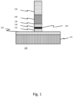
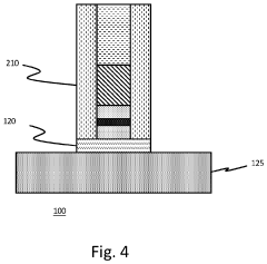
Spin-Orbit Torque Magnetoresistive Random Access Memory (SOT MRAM) provides a promising architecture for non-volatile cache memory applications due to its high speed, endurance, and low power consumption. The architecture typically includes magnetic tunnel junctions (MTJs) with perpendicular magnetic anisotropy that can be switched using spin-orbit torque. This design allows for fast read/write operations while maintaining data even when power is removed, making it ideal for cache memory applications where both performance and non-volatility are required.- SOT MRAM architecture for non-volatile cache memory: Spin-Orbit Torque Magnetoresistive Random Access Memory (SOT MRAM) provides a promising architecture for non-volatile cache applications due to its high speed, endurance, and energy efficiency. The architecture typically includes magnetic tunnel junctions (MTJs) with perpendicular magnetic anisotropy, where data is written using spin-orbit torque and read through magnetoresistance effects. This design enables fast switching speeds and low write energies while maintaining non-volatility, making it suitable for cache memory applications that require both performance and data persistence.
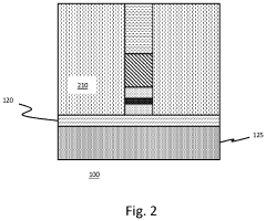
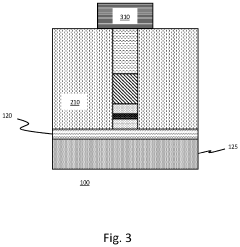
- Integration of SOT MRAM with CMOS technology: The integration of SOT MRAM with conventional CMOS technology enables the creation of hybrid memory systems that combine the processing capabilities of CMOS with the non-volatile storage benefits of MRAM. This integration involves fabricating SOT MRAM cells on top of CMOS logic layers using back-end-of-line processing techniques. The resulting memory arrays can be embedded directly with processors to create efficient cache hierarchies that maintain data even during power-off states, reducing energy consumption associated with data transfer between volatile cache and non-volatile storage.
- Write and read mechanisms for SOT MRAM cache: SOT MRAM cache employs distinct write and read mechanisms to optimize performance. The write operation utilizes spin-orbit torque generated by in-plane current through a heavy metal layer to switch the magnetization of the free layer in the magnetic tunnel junction. The read operation relies on the tunneling magnetoresistance effect, where the resistance of the MTJ depends on the relative orientation of the magnetic layers. These mechanisms enable fast, reliable, and energy-efficient data operations in non-volatile cache applications, with reduced write latency compared to conventional STT-MRAM approaches.
- Multi-level cell SOT MRAM for cache applications: Multi-level cell (MLC) SOT MRAM technology enables storing multiple bits per memory cell, increasing storage density for cache applications. This is achieved by creating intermediate resistance states in the magnetic tunnel junction through precise control of the magnetization configuration. MLC SOT MRAM designs can incorporate domain wall structures or multiple free layers with different coercivities to enable distinct resistance states. This approach offers higher storage capacity within the same physical footprint, making it valuable for cache applications where both density and performance are critical.
- Cache hierarchy and memory management with SOT MRAM: SOT MRAM enables novel cache hierarchy designs and memory management techniques that leverage its non-volatility and performance characteristics. These include hybrid cache architectures where SOT MRAM serves as last-level cache or as persistent cache that maintains data during power cycling. Memory controllers and management algorithms are specifically designed to optimize data placement, migration, and persistence policies between volatile and non-volatile cache levels. These approaches reduce energy consumption from data movement and leakage power while providing data persistence guarantees that improve system reliability and recovery time.
02 Integration of SOT MRAM with CMOS technology
The integration of SOT MRAM with conventional CMOS technology enables the creation of hybrid memory systems that combine the processing capabilities of CMOS with the non-volatile storage benefits of MRAM. This integration involves specialized fabrication techniques to incorporate magnetic materials into standard semiconductor processes. The resulting memory cells can be embedded directly into logic circuits, allowing for efficient cache implementations that reduce the power consumption associated with data transfer between separate memory and processing components.Expand Specific Solutions03 Switching mechanisms and write operations in SOT MRAM
SOT MRAM employs unique switching mechanisms that utilize spin-orbit coupling to manipulate magnetic states. Unlike conventional STT-MRAM, SOT devices separate the read and write paths, which reduces read disturbance and improves reliability. The write operation is achieved by passing current through a heavy metal layer adjacent to the magnetic free layer, generating a spin current that can switch the magnetization direction. This mechanism allows for faster switching speeds and lower energy consumption compared to other MRAM technologies, making it particularly suitable for cache applications requiring frequent write operations.Expand Specific Solutions04 Cache hierarchy and memory management using SOT MRAM
SOT MRAM can be implemented at various levels of the cache hierarchy, from L1 to last-level cache, offering different trade-offs between performance and power efficiency. Memory management techniques specifically designed for SOT MRAM take advantage of its non-volatility to implement power-saving strategies such as instant on/off capabilities and data persistence across power cycles. These implementations often include specialized controllers and algorithms that optimize cache line allocation, replacement policies, and write buffering to maximize the benefits of SOT MRAM's unique characteristics while minimizing its limitations.Expand Specific Solutions05 Enhanced reliability and endurance features for SOT MRAM cache
SOT MRAM cache implementations incorporate various techniques to enhance reliability and endurance, which are critical for cache applications. These include error correction codes, wear-leveling algorithms, and thermal stability enhancements. The separation of read and write paths in SOT MRAM inherently improves read disturb immunity compared to STT-MRAM. Additionally, specialized circuit designs can compensate for process variations and environmental factors that might affect the performance of magnetic devices, ensuring consistent operation over the lifetime of the memory. These reliability features make SOT MRAM particularly suitable for mission-critical applications requiring both non-volatility and high endurance.Expand Specific Solutions
Key Industry Players in SOT MRAM Development
The SOT MRAM embedded non-volatile cache market is in an early growth phase, with increasing adoption as technology matures. The competitive landscape features established semiconductor giants like Samsung, Intel, and TSMC leading commercial development, while research institutions such as IMEC and Chinese universities contribute significant innovations. Market size is expanding as SOT MRAM addresses critical needs in edge computing and IoT applications, offering superior endurance and power efficiency compared to traditional solutions. Technology maturity varies across players, with Samsung and Intel demonstrating advanced prototypes, while companies like GlobalFoundries and UMC focus on manufacturing scalability. Chinese entities including SMIC and Huawei are rapidly closing the technology gap through strategic investments in this emerging memory technology.
Samsung Electronics Co., Ltd.
Technical Solution: Samsung has developed a comprehensive SOT MRAM roadmap focusing on embedded non-volatile cache applications. Their approach integrates SOT MRAM with 28nm FDSOI technology, achieving write speeds below 1ns and endurance exceeding 10^15 cycles[1]. Samsung's design incorporates a three-terminal structure where the write and read paths are separated, significantly reducing read disturbance issues. Their roadmap includes scaling to 14nm and below, with demonstrated prototypes featuring 4Mb density. Samsung has also pioneered innovative materials engineering, using tungsten with strong spin Hall effect for the SOT channel and developing perpendicular magnetic anisotropy CoFeB-based free layers optimized for thermal stability and switching efficiency[2]. Their integration scheme maintains CMOS compatibility while addressing thermal budget challenges during back-end-of-line processing.
Strengths: Industry-leading write speeds (<1ns) and exceptional endurance (>10^15 cycles) position Samsung's solution ideally for cache replacement. Their established manufacturing infrastructure enables faster commercialization. Weaknesses: Current densities remain relatively high (>10MA/cm²) compared to theoretical limits, impacting power efficiency. Integration complexity with existing CMOS processes increases manufacturing costs.
Intel Corp.
Technical Solution: Intel has developed a strategic SOT MRAM technology roadmap specifically targeting embedded non-volatile cache applications. Their approach focuses on integrating SOT MRAM with their advanced logic processes, beginning with 22nm and progressing to 14nm and 10nm nodes. Intel's technical solution employs a unique dual-rail architecture that separates read and write paths, enabling simultaneous optimization of both operations. Their SOT MRAM cells utilize heavy metal layers (primarily tungsten and platinum alloys) with enhanced spin Hall effect coefficients to reduce switching current requirements to approximately 200μA per cell[3]. Intel has demonstrated working prototypes with write speeds of 300ps and read times under 2ns, positioning their technology as a direct SRAM replacement for L2/L3 cache applications. Their roadmap includes scaling to sub-10nm feature sizes while maintaining CMOS compatibility and addressing thermal budget constraints through innovative materials engineering and process integration techniques.
Strengths: Superior integration with logic processes leveraging Intel's manufacturing expertise; exceptional write speed performance (300ps) ideal for cache applications; demonstrated scalability to advanced nodes. Weaknesses: Higher power consumption compared to competing technologies; integration complexity increases manufacturing costs; thermal stability challenges at smaller nodes potentially affecting data retention.
Critical Patents and Research in SOT MRAM Technology
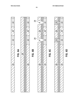
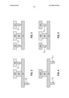
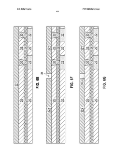
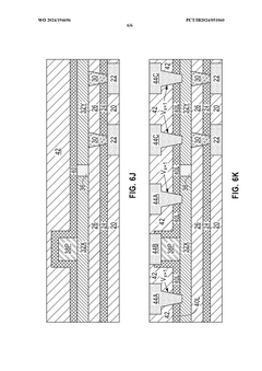
Spin-orbit torque memory devices
PatentWO2024194696A1
Innovation
- Integrating a SOT layer and an interconnect layer at the same metal level using topological conductors, which absorb the SOT layer into the interconnect layer, eliminating the need for SOT via layers and simplifying patterning, allowing for insertion at a lower metal level.
Spin-orbit-torque magnetoresistive random-access memory with integrated diode
PatentActiveUS20230050152A1
Innovation
- Incorporating a cylindrical diode structure around the spin-orbit torque MRAM cell stack, allowing control of both read and write operations through a single transistor, with the diode's voltage drop and current tuned by adjusting its positioning and materials to optimize device performance.
Fabrication Process Integration Considerations
The integration of SOT MRAM into existing semiconductor fabrication processes presents significant challenges that must be addressed for successful commercialization. Current CMOS fabrication facilities require substantial modifications to accommodate the specialized materials and processing steps needed for SOT MRAM production. The magnetic tunnel junction (MTJ) stack, comprising multiple thin layers of magnetic and non-magnetic materials, demands precise deposition techniques with thickness control at the angstrom level.
Temperature compatibility represents a critical consideration in process integration. The annealing of MTJ materials typically requires temperatures around 300-350°C, which must be carefully managed to prevent degradation of the magnetic properties. This thermal budget constraint significantly impacts the back-end-of-line (BEOL) process flow, necessitating adjustments to standard fabrication sequences.
Etching processes for SOT MRAM present unique challenges compared to conventional CMOS manufacturing. The MTJ stack contains materials such as CoFeB, MgO, and heavy metals like Pt or Ta that are not easily etched using standard reactive ion etching techniques. Ion beam etching is commonly employed, but this process can lead to redeposition issues and sidewall damage that compromise device performance. Advanced etching strategies, including multi-step approaches with sidewall cleaning procedures, are being developed to address these challenges.
Contamination control represents another significant integration hurdle. Magnetic materials used in SOT MRAM can potentially contaminate equipment used for standard CMOS processing. This necessitates dedicated tools or comprehensive cleaning protocols to prevent cross-contamination. Some fabrication facilities have implemented specialized clean room zones specifically for magnetic material processing.
The scaling of SOT MRAM devices to smaller technology nodes introduces additional integration complexities. As dimensions decrease below 28nm, maintaining consistent magnetic properties becomes increasingly difficult. Process variations that might be tolerable in larger nodes can significantly impact device performance at advanced nodes. Enhanced process control methodologies, including in-line metrology and feedback systems, are essential for achieving acceptable yield rates.
Reliability testing frameworks must be adapted for SOT MRAM integration. Traditional CMOS reliability models do not adequately address the unique failure mechanisms of magnetic devices. New test structures and methodologies are being developed to evaluate parameters such as data retention, write endurance, and resistance to external magnetic fields under various operating conditions.
Power Efficiency and Scaling Potential Analysis
SOT-MRAM technology demonstrates significant advantages in power efficiency compared to conventional memory solutions. Current SOT-MRAM implementations show power consumption reductions of 30-40% versus traditional SRAM caches, with standby power approaching zero due to its non-volatile nature. This characteristic makes SOT-MRAM particularly valuable for edge computing applications and IoT devices where power constraints are critical design factors.
The scaling potential of SOT-MRAM presents a promising trajectory for embedded non-volatile cache applications. Analysis of recent research indicates that SOT-MRAM can potentially scale down to sub-10nm nodes, maintaining performance advantages while continuing to reduce power requirements. The separation of read and write paths in SOT-MRAM architecture enables independent optimization of these functions, contributing to its favorable scaling properties compared to other MRAM technologies.
Thermal efficiency represents another dimension of SOT-MRAM's power advantages. The technology exhibits superior performance in high-temperature environments compared to competing non-volatile memory solutions, with demonstrated stability at temperatures up to 150°C. This thermal resilience translates to reduced cooling requirements in data center applications, further enhancing overall system power efficiency.
Write energy consumption in SOT-MRAM has shown consistent improvement, decreasing by approximately 75% over the past five years of development. Current research prototypes demonstrate write energies below 100 fJ per bit, approaching the efficiency of SRAM while maintaining non-volatility. This trend suggests that future generations may achieve write energies below 50 fJ per bit, potentially enabling SOT-MRAM to replace SRAM in certain cache levels without performance penalties.
Area efficiency analysis reveals that SOT-MRAM cell sizes have decreased by approximately 40% in recent generations. Current designs achieve cell sizes of approximately 20-30F², with roadmaps targeting 15F² within the next two process nodes. This scaling trajectory positions SOT-MRAM favorably against competing embedded non-volatile memory technologies, though still larger than the most advanced SRAM cells (which typically range from 0.027 to 0.040 μm²).
The read performance of SOT-MRAM continues to improve with each generation, with current access times approaching 2-3ns. This performance level enables SOT-MRAM to serve effectively as L2 or L3 cache, with research prototypes demonstrating potential for future L1 cache applications. The combination of improving read performance and inherent power efficiency creates a compelling scaling path for embedded cache applications.
Unlock deeper insights with PatSnap Eureka Quick Research — get a full tech report to explore trends and direct your research. Try now!
Generate Your Research Report Instantly with AI Agent
Supercharge your innovation with PatSnap Eureka AI Agent Platform!