Applications of Polysilane in Film Technology
JUL 11, 20259 MIN READ
Generate Your Research Report Instantly with AI Agent
Patsnap Eureka helps you evaluate technical feasibility & market potential.
Polysilane Film Tech Evolution and Objectives
Polysilane, a class of silicon-based polymers, has emerged as a promising material in film technology over the past few decades. The evolution of polysilane film technology can be traced back to the 1980s when researchers first discovered the unique electronic and optical properties of these materials. Since then, the field has witnessed significant advancements, driven by the growing demand for high-performance electronic and optoelectronic devices.
The initial focus of polysilane research was on understanding the fundamental properties of these materials, including their molecular structure, electronic band structure, and photophysical characteristics. As knowledge in this area expanded, researchers began to explore potential applications in various fields, particularly in thin-film technologies. The ability to form stable, uniform films with tunable properties made polysilanes attractive candidates for a wide range of applications.
One of the key objectives in polysilane film technology has been to improve the processability and stability of these materials. Early polysilanes were often difficult to work with due to their sensitivity to air and moisture. Researchers have made significant strides in developing more robust polysilane structures and optimizing film deposition techniques to overcome these challenges. This has led to the development of polysilane films with enhanced thermal and chemical stability, making them suitable for use in more demanding applications.
Another important goal in the field has been to exploit the unique electronic properties of polysilanes for advanced electronic and optoelectronic devices. The σ-conjugated backbone of polysilanes gives rise to interesting electronic and photonic properties, making them potential candidates for applications such as organic light-emitting diodes (OLEDs), photovoltaic cells, and field-effect transistors. Researchers have been working on tailoring the electronic properties of polysilane films through molecular design and doping strategies to optimize their performance in these applications.
In recent years, there has been a growing interest in exploring the potential of polysilane films in emerging technologies such as flexible electronics and wearable devices. The ability to form thin, flexible films with good electrical and optical properties makes polysilanes attractive materials for these applications. Researchers are now focusing on developing new polysilane structures and processing techniques that can meet the specific requirements of flexible and stretchable electronics.
Looking ahead, the objectives of polysilane film technology research are likely to include further improvements in material stability and processability, as well as the development of new functionalities through molecular engineering. There is also a growing emphasis on sustainable and environmentally friendly materials, which may drive research into bio-based or recyclable polysilane derivatives. As the field continues to evolve, it is expected that polysilane films will find new applications in areas such as sensors, energy storage devices, and advanced coatings, further expanding their technological impact.
Market Demand for Polysilane Films
The market demand for polysilane films has been steadily growing in recent years, driven by their unique properties and diverse applications across various industries. Polysilanes, a class of silicon-based polymers, have garnered significant attention due to their excellent optical and electronic properties, making them particularly attractive for use in advanced film technologies.
In the electronics industry, polysilane films have found applications in the production of organic light-emitting diodes (OLEDs) and photovoltaic devices. The increasing demand for high-performance displays and renewable energy solutions has created a substantial market for polysilane-based materials. As the global OLED market continues to expand, with projections indicating robust growth over the next decade, the demand for polysilane films is expected to rise correspondingly.
The semiconductor industry has also shown keen interest in polysilane films for their potential use in lithography and as precursors for silicon carbide production. With the ongoing miniaturization of electronic components and the push for more efficient semiconductor manufacturing processes, polysilane films offer promising solutions to address these technological challenges.
In the field of optics and photonics, polysilane films have demonstrated potential for use in optical waveguides, nonlinear optical materials, and photoresists. The growing demand for advanced optical components in telecommunications, data centers, and sensing applications is likely to drive further adoption of polysilane-based materials.
The automotive sector represents another significant market for polysilane films, particularly in the development of smart windows and advanced coatings. As the automotive industry shifts towards more energy-efficient and technologically advanced vehicles, the demand for materials that can enhance performance and functionality is expected to increase.
Furthermore, the aerospace and defense industries have shown interest in polysilane films for their potential applications in protective coatings, thermal management, and advanced sensors. The unique properties of polysilanes, such as their thermal stability and radiation resistance, make them attractive for use in extreme environments.
While the market demand for polysilane films is promising, it is important to note that challenges remain in terms of scalability and cost-effectiveness. As research and development efforts continue to address these issues, the market is expected to expand further, with new applications and industries potentially adopting polysilane-based technologies.
In conclusion, the market demand for polysilane films is driven by their versatility and unique properties, with applications spanning multiple industries. As technological advancements continue and new applications emerge, the demand for these materials is likely to grow, presenting opportunities for innovation and market expansion in the field of film technology.
Polysilane Film Tech Challenges
Polysilane films have emerged as a promising material in various technological applications, yet their widespread adoption faces several significant challenges. One of the primary obstacles is the inherent instability of polysilane structures when exposed to ultraviolet (UV) light. This photosensitivity can lead to degradation of the film's properties over time, limiting its longevity and reliability in applications requiring prolonged exposure to light.
Another major challenge lies in the precise control of film thickness and uniformity during the deposition process. Achieving consistent and ultra-thin polysilane films with nanometer-scale precision remains a complex task, often resulting in variations that can affect the film's performance in electronic and optical devices. This issue is particularly critical in the development of high-performance thin-film transistors and photovoltaic cells.
The synthesis of high-molecular-weight polysilanes with controlled molecular architecture presents another significant hurdle. Current synthetic methods often yield polymers with broad molecular weight distributions, which can lead to inconsistent film properties and performance. Developing more refined polymerization techniques to produce well-defined polysilane structures is crucial for enhancing the material's applicability in advanced technologies.
Furthermore, the integration of polysilane films with other materials and existing manufacturing processes poses considerable challenges. Compatibility issues may arise when incorporating polysilane films into multilayer device structures, particularly in terms of adhesion, thermal stability, and chemical resistance. Overcoming these integration challenges is essential for the successful implementation of polysilane-based technologies in commercial applications.
The environmental stability of polysilane films also remains a concern. While these materials show promise in various applications, their susceptibility to oxidation and hydrolysis in ambient conditions can limit their practical use. Developing effective encapsulation methods or chemical modifications to enhance the environmental resilience of polysilane films is an ongoing area of research.
Lastly, the scalability of polysilane film production presents a significant challenge for industrial applications. Current laboratory-scale synthesis and deposition techniques may not be directly transferable to large-scale manufacturing processes. Developing cost-effective and efficient methods for mass production of high-quality polysilane films is crucial for their commercial viability in various technological applications.
Current Polysilane Film Solutions
01 Synthesis and properties of polysilanes
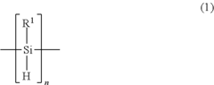
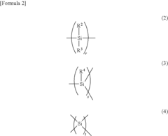
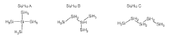
Polysilanes are synthesized through various methods and exhibit unique properties. These silicon-based polymers have applications in electronics, optics, and materials science due to their electronic and optical characteristics. The synthesis and modification of polysilanes can be tailored to achieve specific properties for different applications.- Synthesis and properties of polysilanes: Polysilanes are silicon-based polymers with unique electronic and optical properties. They can be synthesized through various methods, including Wurtz coupling of dichlorosilanes. These polymers exhibit interesting characteristics such as photoconductivity and photoluminescence, making them suitable for various applications in electronics and optics.
- Applications of polysilanes in coatings and films: Polysilanes can be used to create functional coatings and thin films with specific properties. These materials can be applied to various substrates to impart characteristics such as improved adhesion, chemical resistance, or optical properties. The versatility of polysilanes allows for their use in diverse applications, including protective coatings and optical devices.
- Polysilanes in photoresist materials: Polysilanes have found applications in photoresist materials for semiconductor manufacturing. Their unique photosensitive properties make them suitable for use in lithography processes. When exposed to light, polysilanes can undergo chemical changes, allowing for the creation of precise patterns on semiconductor substrates.
- Modification and functionalization of polysilanes: Polysilanes can be modified and functionalized to enhance their properties or introduce new functionalities. This can involve the incorporation of various side groups or the creation of copolymers with other materials. Such modifications allow for the tailoring of polysilanes for specific applications or to improve their performance in existing uses.
- Polysilanes in electronic and optoelectronic devices: The unique electronic properties of polysilanes make them suitable for use in various electronic and optoelectronic devices. They can be incorporated into components such as organic light-emitting diodes (OLEDs), solar cells, and transistors. The ability to tune the electronic properties of polysilanes through structural modifications allows for their optimization in these applications.
02 Polysilanes in photoresist and lithography applications
Polysilanes are utilized in photoresist formulations and lithography processes. Their photosensitive nature and ability to form stable patterns make them suitable for semiconductor manufacturing and microfabrication. These materials can be used to create high-resolution patterns and structures in various electronic and optical devices.Expand Specific Solutions03 Polysilane-based coatings and films
Polysilanes are employed in the development of coatings and thin films. These materials can be applied to various substrates to impart specific properties such as improved durability, chemical resistance, or optical characteristics. The coatings and films find applications in areas like protective layers, optical coatings, and electronic components.Expand Specific Solutions04 Functionalization and modification of polysilanes
Polysilanes can be functionalized and modified to enhance their properties or introduce new functionalities. This includes the incorporation of various side groups, crosslinking agents, or other reactive moieties. These modifications allow for the tailoring of polysilanes for specific applications or to improve their compatibility with other materials.Expand Specific Solutions05 Polysilanes in composite materials
Polysilanes are used in the development of composite materials, where they are combined with other polymers or inorganic materials. These composites can exhibit enhanced mechanical, thermal, or electrical properties compared to the individual components. The incorporation of polysilanes in composites opens up new possibilities for advanced materials in various industries.Expand Specific Solutions
Key Players in Polysilane Film Industry
The applications of polysilane in film technology represent an emerging field with significant potential for growth. The market is currently in its early stages of development, with a relatively small but expanding market size. Technological maturity is still evolving, with ongoing research and development efforts across academia and industry. Key players in this space include established chemical companies like Air Liquide SA, JSR Corp., and Nippon Paint Co., Ltd., who are leveraging their expertise in materials science to explore polysilane applications. Additionally, research institutions such as Qingdao University of Science & Technology and Kanazawa University are contributing to advancing the fundamental understanding and practical applications of polysilane in film technology. As the technology progresses, we can expect increased collaboration between industry and academia to drive innovation and commercialization in this promising field.
JSR Corp.
Technical Solution: JSR Corp. has developed advanced polysilane-based materials for film technology applications. Their approach involves synthesizing novel polysilane derivatives with tailored molecular structures to enhance optical and electronic properties. JSR's polysilane films exhibit high transparency in the UV-visible range and tunable refractive indices, making them suitable for anti-reflective coatings and optical waveguides [1]. The company has also explored the use of polysilanes as photoresists for lithography, leveraging their photosensitivity and ability to form well-defined patterns upon UV exposure [3]. Additionally, JSR has investigated polysilane-based hole transport layers for organic light-emitting diodes (OLEDs), taking advantage of the material's semiconducting properties and charge carrier mobility [5].
Strengths: Versatile applications in optics and electronics, customizable material properties. Weaknesses: Potential stability issues under prolonged UV exposure, limited commercial scale production.
Merck Patent GmbH
Technical Solution: Merck Patent GmbH has focused on developing polysilane-based materials for advanced electronic and optoelectronic applications in film technology. Their research has led to the creation of high-performance polysilane thin films with enhanced charge transport properties, suitable for use in organic field-effect transistors (OFETs) and photovoltaic devices [2]. Merck's approach involves precise control of the polysilane molecular weight and side-chain functionalization to optimize film morphology and electronic characteristics. They have also explored the incorporation of nanoparticles into polysilane matrices to create hybrid materials with improved thermal stability and conductivity [4]. Furthermore, Merck has developed novel crosslinking strategies for polysilane films, enabling the formation of robust, insoluble networks with enhanced mechanical properties and resistance to environmental degradation [6].
Strengths: High-performance electronic materials, innovative hybrid and crosslinked structures. Weaknesses: Potentially high production costs, limited large-scale manufacturing experience.
Polysilane Film Core Innovations
Polysilane and polysilane-containing resin composition
PatentInactiveUS8163863B2
Innovation
- Introducing a Si—H group into the polysilane main chain and bonding a hydrosilylatable compound with functional groups like hydroxyl, carboxyl, or epoxy groups, allowing for controlled hydrosilylation to enhance solubility and reactivity without complex steps or special apparatus.


Process for producing liquid polysilanes and isomer enriched higher silanes
PatentWO2020077183A1
Innovation
- The synthesis of higher silanes involves catalytic transformation of lower silanes using heterogeneous catalysts, such as Group I, II, or III element-based catalysts, to control temperature, residence time, and reactant ratios, resulting in isomerically enriched polysilanes with specific isomer ratios and high purity.
Environmental Impact of Polysilane Films
The environmental impact of polysilane films is a critical consideration in their application within film technology. These films, while offering unique properties and potential benefits, also pose certain environmental challenges that must be carefully evaluated and addressed.
Polysilane films, being synthetic materials, have implications for resource consumption and waste generation throughout their lifecycle. The production process of polysilanes involves the use of various chemicals and energy-intensive manufacturing techniques, which can contribute to carbon emissions and resource depletion. However, the long-lasting nature of polysilane films may offset some of these initial environmental costs by reducing the need for frequent replacements.
One of the primary environmental concerns associated with polysilane films is their end-of-life disposal. Unlike some biodegradable alternatives, polysilane films do not readily decompose in natural environments. This persistence can lead to accumulation in landfills or, if improperly disposed of, contribute to environmental pollution. Efforts are being made to develop more environmentally friendly disposal methods, including chemical recycling processes that break down polysilanes into reusable components.
On the positive side, polysilane films have shown potential in enhancing the efficiency of solar cells and other energy-harvesting devices. This application could indirectly contribute to reducing reliance on fossil fuels and mitigating climate change impacts. Additionally, the durability and protective properties of polysilane films can extend the lifespan of various products, potentially reducing overall material consumption and waste generation.
The production of polysilane films also raises concerns about the release of volatile organic compounds (VOCs) during manufacturing and application processes. These emissions can contribute to air pollution and have potential health impacts on workers and surrounding communities. Ongoing research is focused on developing low-VOC formulations and improving manufacturing processes to minimize these emissions.
Water pollution is another environmental aspect to consider. The synthesis and processing of polysilanes may involve the use of solvents and other chemicals that, if not properly managed, could contaminate water sources. Implementing robust waste management systems and exploring water-based alternatives are crucial steps in mitigating this risk.
As the use of polysilane films expands, there is a growing emphasis on life cycle assessments to comprehensively evaluate their environmental footprint. These assessments consider factors such as raw material extraction, energy consumption, emissions, and disposal, providing a holistic view of the environmental impact. Such analyses are essential for guiding the development of more sustainable polysilane film technologies and informing policy decisions regarding their use and regulation.
Polysilane Film Manufacturing Processes
Polysilane film manufacturing processes have evolved significantly over the years, incorporating various techniques to optimize the production of high-quality films for diverse applications. The most common methods include spin coating, dip coating, and chemical vapor deposition (CVD).
Spin coating is widely used for producing thin, uniform polysilane films. This process involves depositing a solution of polysilane onto a substrate, which is then rotated at high speed to spread the material evenly. The solvent evaporates during spinning, leaving behind a thin film. Spin coating allows for precise control over film thickness and uniformity, making it ideal for applications requiring nanometer-scale precision.
Dip coating offers a simpler alternative for larger substrates or when precise thickness control is less critical. In this method, the substrate is immersed in a polysilane solution and then withdrawn at a controlled rate. The film thickness is primarily determined by the withdrawal speed and solution viscosity. While less precise than spin coating, dip coating can produce films with good uniformity over large areas.
Chemical vapor deposition (CVD) is a more advanced technique for polysilane film production. This process involves introducing gaseous precursors into a reaction chamber, where they decompose and deposit onto a heated substrate. CVD allows for the creation of highly pure and conformal polysilane films, even on complex substrate geometries. However, it requires specialized equipment and careful control of process parameters.
Recent advancements in polysilane film manufacturing have focused on improving film quality, increasing production efficiency, and expanding the range of achievable properties. One notable development is the use of plasma-enhanced CVD (PECVD), which enables lower deposition temperatures and faster growth rates compared to traditional CVD methods.
Another emerging technique is electrospray deposition, which offers precise control over film thickness and morphology. This method involves applying a high voltage to a polysilane solution, creating a fine mist of charged droplets that are attracted to the substrate. Electrospray deposition shows promise for creating structured polysilane films with unique optical and electronic properties.
Researchers are also exploring novel approaches to enhance the properties of polysilane films during the manufacturing process. These include in-situ crosslinking techniques to improve thermal stability and mechanical strength, as well as the incorporation of nanoparticles or other functional materials to create composite films with tailored properties.
As the demand for advanced polysilane films continues to grow in various industries, ongoing research and development efforts are focused on scaling up production processes while maintaining film quality and consistency. This includes the development of roll-to-roll manufacturing techniques for continuous production of large-area polysilane films, as well as the integration of real-time monitoring and control systems to ensure consistent film properties across batches.
Unlock deeper insights with Patsnap Eureka Quick Research — get a full tech report to explore trends and direct your research. Try now!
Generate Your Research Report Instantly with AI Agent
Supercharge your innovation with Patsnap Eureka AI Agent Platform!