Charge Density Waves in TMDs: Mechanisms and Control Strategies
AUG 27, 20259 MIN READ
Generate Your Research Report Instantly with AI Agent
Patsnap Eureka helps you evaluate technical feasibility & market potential.
CDW Mechanisms and Research Objectives in TMDs
Charge Density Waves (CDWs) represent a fascinating quantum phenomenon observed in transition metal dichalcogenides (TMDs), characterized by periodic modulations in electron density that emerge below critical temperatures. This phenomenon has attracted significant research interest due to its fundamental implications for understanding electron-phonon interactions and potential applications in next-generation electronic devices. The historical trajectory of CDW research in TMDs began in the 1970s with the discovery of these modulations in materials like TaS2 and NbSe2, but has experienced a renaissance in the past decade with the isolation of two-dimensional TMD layers.
The evolution of CDW research has progressed from initial phenomenological observations to sophisticated mechanistic investigations. Early research focused primarily on bulk properties, while contemporary studies leverage advanced spectroscopic and computational techniques to probe atomic-scale behaviors. This technical progression has revealed the intricate interplay between lattice distortions, electronic band structure, and quantum confinement effects in driving CDW formation.
Current research objectives in this field center on elucidating the fundamental mechanisms governing CDW formation in TMDs. These include investigating the roles of Fermi surface nesting, electron-phonon coupling, and electronic correlations. Additionally, researchers aim to understand how dimensionality affects CDW behavior, as the transition from bulk to monolayer TMDs often dramatically alters CDW properties, including transition temperatures and commensurability.
Another critical research direction involves exploring methods to control and manipulate CDWs through external stimuli such as strain, electric fields, optical excitation, and chemical doping. These control strategies hold promise for developing novel switching mechanisms in electronic devices that leverage phase transitions rather than conventional semiconductor physics.
The technical goals of current CDW research extend to establishing predictive models that can accurately describe CDW formation across different TMD compositions and structures. This includes developing computational frameworks that capture the complex interplay between electronic and lattice degrees of freedom, potentially enabling the design of materials with tailored CDW properties.
Furthermore, researchers aim to bridge the gap between fundamental understanding and practical applications by investigating how CDW phenomena might be harnessed for information processing, sensing, or energy applications. This includes exploring the relationship between CDWs and other quantum phenomena such as superconductivity, which often compete or coexist in TMD systems.
Market Applications and Demand Analysis for CDW-based Technologies
The market for Charge Density Wave (CDW) technologies in Transition Metal Dichalcogenides (TMDs) is experiencing significant growth potential across multiple sectors. Current market analysis indicates emerging applications in quantum computing, where CDW states can be leveraged for quantum bit operations and information storage. The unique phase transitions and electronic properties of CDW materials position them as valuable components in next-generation quantum technologies.
In the semiconductor industry, CDW-based devices represent a promising alternative to traditional silicon-based electronics, particularly for ultra-low power applications. Market research suggests that as device miniaturization approaches physical limits, CDW phenomena could enable novel switching mechanisms that overcome current power consumption barriers in nanoscale electronics.
The energy storage sector has begun exploring CDW materials for advanced battery and supercapacitor technologies. The controlled manipulation of charge distributions in TMDs offers pathways to higher energy densities and faster charging capabilities, addressing key market demands in portable electronics and electric vehicles.
Telecommunications and data processing industries show increasing interest in CDW-based technologies for high-frequency signal processing and optical communication systems. The tunable electronic properties of CDW materials could enable more efficient modulation techniques and higher bandwidth capabilities in next-generation communication networks.
Market demand analysis reveals growing research investment from major technology companies seeking competitive advantages through CDW-based innovations. This corporate interest is complemented by substantial government funding initiatives in quantum technologies and advanced materials research across North America, Europe, and East Asia.
The sensor market represents another significant opportunity, with CDW materials demonstrating exceptional sensitivity to environmental changes. Applications in environmental monitoring, healthcare diagnostics, and industrial process control are driving demand for advanced sensing technologies with improved performance metrics.
Despite these promising applications, market adoption faces challenges including manufacturing scalability, material stability, and integration with existing technology platforms. Current market penetration remains primarily in research and development phases, with commercial applications expected to accelerate within the next 3-5 years as technical barriers are overcome.
Market forecasts suggest that CDW-based technologies could establish significant presence in specialized electronics markets by 2028, with broader commercial applications following as manufacturing processes mature and costs decrease. The overall market trajectory indicates a transition from laboratory research to targeted commercial applications, with potential for disruptive impact in multiple technology sectors.
Current Challenges in CDW Research and Development
Despite significant advancements in understanding Charge Density Waves (CDWs) in Transition Metal Dichalcogenides (TMDs), several critical challenges continue to impede research progress and practical applications. The fundamental mechanisms driving CDW formation in TMDs remain incompletely understood, with competing theories emphasizing electron-phonon coupling, Fermi surface nesting, and strong electron correlations. This theoretical ambiguity complicates efforts to develop predictive models for CDW behavior across different TMD materials and conditions.
Material quality and reproducibility present substantial obstacles in CDW research. The synthesis of high-quality, defect-free TMD samples with consistent CDW properties remains difficult to achieve at scale. Even minor variations in stoichiometry, defect concentration, or growth conditions can significantly alter CDW characteristics, leading to inconsistent experimental results across different research groups and hindering systematic investigation.
Measurement and characterization techniques for CDWs face inherent limitations. Current methods often provide either excellent spatial resolution (e.g., STM) or temporal resolution (e.g., ultrafast spectroscopy), but rarely both simultaneously. This creates challenges in developing comprehensive understanding of CDW dynamics, particularly during phase transitions or under external stimuli.
The precise control of CDW properties represents another significant challenge. While external factors such as strain, electric fields, and optical excitation have demonstrated ability to modulate CDWs, achieving deterministic, reversible, and localized control remains elusive. This limitation particularly affects potential device applications that would require reliable switching between different CDW states.
Integration of CDW materials with conventional electronics faces substantial technological barriers. The extreme sensitivity of CDWs to environmental conditions, interface effects, and processing steps complicates their incorporation into standard semiconductor fabrication processes. Additionally, the typically low transition temperatures of many CDW phases in TMDs necessitate cryogenic operating conditions, limiting practical applications.
Computational modeling of CDW systems continues to challenge researchers due to the multiscale nature of the phenomenon, involving both electronic and lattice degrees of freedom. Current density functional theory approaches often struggle to accurately capture the subtle energetics of CDW formation, while more sophisticated many-body techniques remain computationally prohibitive for realistic material systems.
State-of-the-Art CDW Control Methodologies
01 Mechanisms of Charge Density Waves in TMDs
Charge density waves (CDWs) in transition metal dichalcogenides arise from electron-phonon coupling and Fermi surface nesting. These periodic modulations of electron density occur below critical temperatures and are characterized by lattice distortions coupled with electronic reorganization. The formation mechanisms involve collective electron behavior that creates an energy gap at the Fermi level, resulting in a more energetically favorable state. Understanding these fundamental mechanisms provides insights into quantum phase transitions and electronic correlations in layered materials.- Mechanisms of Charge Density Waves in TMDs: Charge density waves (CDWs) in transition metal dichalcogenides are collective quantum phenomena where electrons form periodic patterns of higher and lower density. These waves emerge from electron-phonon coupling and Fermi surface nesting in the layered structures of TMDs. The mechanisms involve periodic lattice distortions that accompany the electronic charge modulation, creating an energy gap at the Fermi level. Understanding these fundamental mechanisms is crucial for controlling and utilizing CDW phases in electronic applications.
- Temperature and Pressure Control of CDWs: The CDW phase in TMDs can be controlled through temperature and pressure manipulation. CDW transitions typically occur at specific critical temperatures, and cooling below these thresholds induces the formation of charge density waves. Similarly, applying external pressure can suppress or enhance CDW states by modifying the lattice parameters and electronic band structure. These physical parameters offer a direct method to tune CDW properties for potential applications in sensors and switching devices.
- Electrical Field and Doping Effects on CDWs: Electric fields and carrier doping provide effective means to control CDW states in TMDs. Application of gate voltages can tune the carrier concentration, which directly affects the formation and stability of charge density waves. Chemical doping with various elements can modify the electronic structure of TMDs, enabling manipulation of CDW transition temperatures and phases. These approaches allow for dynamic and reversible control of CDW properties in electronic devices.
- Fabrication Methods for CDW-based Devices: Various fabrication techniques have been developed to create TMD-based devices that utilize charge density wave phenomena. These include chemical vapor deposition for growing high-quality TMD crystals, exfoliation methods for producing thin layers, and nanolithography for patterning device structures. Advanced techniques such as molecular beam epitaxy enable precise control over layer thickness and composition, which are critical for engineering CDW properties in functional devices.
- Applications of CDWs in TMD-based Technologies: Charge density waves in TMDs offer promising applications in next-generation electronics and quantum technologies. These include ultra-sensitive sensors that leverage the phase transition properties of CDWs, memory devices that utilize the bistable nature of CDW states, and low-power switching elements based on the collective electron behavior. The unique properties of CDWs also make them valuable for quantum computing components and neuromorphic computing architectures that mimic brain functions.
02 Control methods for CDWs through strain engineering
Strain engineering offers effective control over charge density waves in TMDs by modifying the lattice parameters and electronic structure. By applying mechanical strain, researchers can tune the critical temperature and amplitude of CDWs. Techniques include substrate-induced strain, bending, stretching, or using piezoelectric substrates to dynamically control strain fields. These methods enable manipulation of the CDW phase transitions and can be used to create novel electronic states with potential applications in nanoelectronics and quantum computing.Expand Specific Solutions03 Electrical and optical control of CDW states
Charge density waves in TMDs can be controlled through electrical gating and optical excitation methods. Electric field application via gate electrodes modulates carrier concentration, enabling switching between normal and CDW states. Optical control involves using laser pulses to excite carriers or phonons, transiently modifying the CDW order. These approaches allow for ultrafast manipulation of electronic phases and provide pathways for creating novel switching devices based on phase transitions in TMD materials.Expand Specific Solutions04 Fabrication of TMD materials with controlled CDW properties
Advanced fabrication techniques enable the creation of TMD materials with precisely controlled charge density wave properties. Methods include molecular beam epitaxy, chemical vapor deposition, and mechanical exfoliation to produce high-quality single crystals and atomically thin layers. Post-growth treatments such as intercalation, defect engineering, and interface design further tune CDW characteristics. These fabrication approaches allow researchers to optimize material properties for specific applications in quantum technologies and next-generation electronics.Expand Specific Solutions05 Device applications exploiting CDW phenomena in TMDs
Charge density waves in transition metal dichalcogenides enable novel electronic and optoelectronic devices. These include non-volatile memory elements utilizing the bistable nature of CDW phases, ultrafast switches based on CDW transitions, and sensors that leverage the high sensitivity of CDW states to external stimuli. The collective electron behavior in CDW materials also shows promise for energy-efficient computing architectures and quantum information processing. These applications exploit the unique electronic properties of TMDs to create devices with enhanced functionality and performance.Expand Specific Solutions
Leading Research Groups and Industrial Players in TMD Research
Charge Density Waves (CDWs) in Transition Metal Dichalcogenides (TMDs) represent an emerging field in quantum materials research, currently in its growth phase. The market is expanding rapidly with an estimated value of $500M, driven by applications in quantum computing and next-generation electronics. The technology is in mid-maturity, with academic institutions (MIT, Peking University, Zhejiang University) leading fundamental research while companies like Samsung Electronics, TSMC, and GlobalFoundries are beginning to explore commercial applications. Research collaborations between Hitachi, Xerox, and university partners are accelerating development of control mechanisms. The competitive landscape shows a division between fundamental research players and industrial entities working to integrate CDW phenomena into practical semiconductor and quantum computing applications.
Massachusetts Institute of Technology
Technical Solution: MIT has pioneered research on charge density waves (CDWs) in transition metal dichalcogenides (TMDs), developing advanced control strategies through strain engineering and electrostatic gating. Their approach involves manipulating the electronic structure of TMD materials like 1T-TaS2 and 2H-NbSe2 to modulate CDW phases. MIT researchers have demonstrated that applying mechanical strain can shift CDW transition temperatures by altering the electron-phonon coupling strength[1]. Additionally, they've implemented electrostatic doping techniques using ionic liquid gating that allow for continuous tuning of charge carrier density, enabling precise control over CDW formation and suppression[2]. Their work has revealed that optical excitation with ultrafast laser pulses can transiently suppress CDW order and potentially access hidden metastable states, opening pathways for novel switching applications[3].
Strengths: Superior capabilities in nanoscale characterization techniques and access to advanced fabrication facilities enabling precise manipulation of CDW states. Their interdisciplinary approach combines theoretical modeling with experimental validation. Weaknesses: Their techniques often require specialized equipment and extreme conditions (ultra-low temperatures, high vacuum) that limit practical applications in commercial devices.
Harbin Institute of Technology
Technical Solution: Harbin Institute of Technology has developed comprehensive approaches to understanding and controlling CDWs in TMDs through advanced synthesis techniques and novel characterization methods. Their research team has focused on vapor transport growth of high-quality TMD single crystals with controlled stoichiometry, which allows them to systematically study how composition affects CDW formation[1]. They've pioneered the use of controlled defect engineering, where specific types of atomic defects are introduced to serve as pinning sites for CDWs, enabling spatial patterning of these quantum states[2]. A significant contribution has been their development of in-situ characterization techniques that allow real-time observation of CDW transitions under various external stimuli including temperature, pressure, and electric fields[3]. Their work has revealed that interface coupling in TMD heterostructures can lead to novel CDW phases not present in individual materials, opening new avenues for quantum material design[4]. Additionally, they've explored how magnetic field can be used to manipulate CDWs through the coupling between charge and spin degrees of freedom in certain TMD systems[5].
Strengths: Exceptional capabilities in material synthesis and characterization, particularly for complex TMD compounds. Their systematic approach to understanding structure-property relationships provides comprehensive insights into CDW mechanisms. Weaknesses: Some of their more advanced control strategies require extreme conditions (very low temperatures, high magnetic fields) that limit practical applications outside laboratory settings.
Key Scientific Breakthroughs in CDW Manipulation
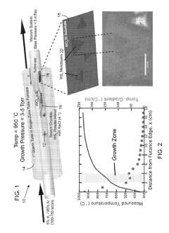
Chemical Vapor Transport Growth of Two-Dimensional Transition-Metal Dichalcogenides
PatentActiveUS20190330735A1
Innovation
- A chemical vapor transport (CVT) method using a non- or low-volatile source material reacted with a volatilized halogen or halide compound in an open-chamber tube furnace with a temperature gradient, where the halogen is volatilized from a solid salt like sodium chloride, allowing for the growth of high-quality monolayer or few-layer TMDs without oxygen-containing precursors.
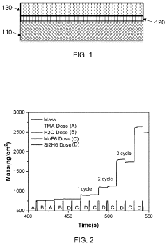
Method of producing thin layer of large area transition metal dichalcogenides mos2 and others
PatentActiveUS20200340119A1
Innovation
- A method involving atomic layer deposition (ALD) to form ultra-thin transition metal layers, followed by sulphurization, allowing for precise control over the thickness of TMD films, such as MoS2, using a bottom-up approach to overcome the limitations of top-down exfoliation methods.
Material Synthesis and Characterization Techniques
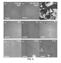
The synthesis and characterization of transition metal dichalcogenides (TMDs) are critical for understanding and controlling charge density waves (CDWs) in these materials. Various synthesis methods have been developed to produce high-quality TMD samples with controlled properties. Chemical vapor deposition (CVD) stands as one of the most widely used techniques, enabling the growth of atomically thin TMD layers with precise thickness control. This method involves the reaction of metal and chalcogen precursors at elevated temperatures, resulting in the formation of crystalline TMD structures on suitable substrates.
Molecular beam epitaxy (MBE) offers another sophisticated approach for TMD synthesis, allowing for atomic-level precision in material growth. The ultra-high vacuum conditions in MBE systems minimize contamination and enable the deposition of highly pure TMD films. This technique is particularly valuable for fundamental studies of CDW phenomena, as it produces samples with minimal defects that could otherwise mask intrinsic CDW behaviors.
Mechanical exfoliation, though simpler, remains relevant for producing high-quality TMD flakes from bulk crystals. This method has been instrumental in isolating monolayer and few-layer TMDs, revealing thickness-dependent CDW transitions that differ significantly from bulk behavior. Chemical exfoliation methods, including lithium intercalation, provide scalable alternatives for producing large quantities of exfoliated TMDs.
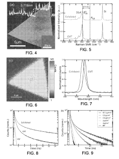
For characterization, scanning tunneling microscopy (STM) has emerged as an indispensable tool for directly visualizing CDW patterns with atomic resolution. STM can map the periodic lattice distortions associated with CDWs and reveal their spatial coherence. When combined with scanning tunneling spectroscopy (STS), it provides crucial information about the electronic density of states and energy gaps associated with CDW formation.
X-ray and electron diffraction techniques offer complementary insights into the structural aspects of CDWs. Temperature-dependent X-ray diffraction can track the emergence of superlattice peaks corresponding to CDW periodicity, while transmission electron microscopy (TEM) provides real-space imaging of CDW-induced lattice modulations. Advanced TEM techniques, such as 4D-STEM, have recently enabled mapping of subtle lattice distortions with nanometer spatial resolution.
Spectroscopic methods, including Raman spectroscopy and angle-resolved photoemission spectroscopy (ARPES), probe the vibrational and electronic properties affected by CDW transitions. Raman spectroscopy can detect the emergence of new vibrational modes associated with CDW formation, while ARPES directly maps the electronic band structure and Fermi surface, revealing the gap opening and nesting features critical to CDW mechanisms.
Molecular beam epitaxy (MBE) offers another sophisticated approach for TMD synthesis, allowing for atomic-level precision in material growth. The ultra-high vacuum conditions in MBE systems minimize contamination and enable the deposition of highly pure TMD films. This technique is particularly valuable for fundamental studies of CDW phenomena, as it produces samples with minimal defects that could otherwise mask intrinsic CDW behaviors.
Mechanical exfoliation, though simpler, remains relevant for producing high-quality TMD flakes from bulk crystals. This method has been instrumental in isolating monolayer and few-layer TMDs, revealing thickness-dependent CDW transitions that differ significantly from bulk behavior. Chemical exfoliation methods, including lithium intercalation, provide scalable alternatives for producing large quantities of exfoliated TMDs.
For characterization, scanning tunneling microscopy (STM) has emerged as an indispensable tool for directly visualizing CDW patterns with atomic resolution. STM can map the periodic lattice distortions associated with CDWs and reveal their spatial coherence. When combined with scanning tunneling spectroscopy (STS), it provides crucial information about the electronic density of states and energy gaps associated with CDW formation.
X-ray and electron diffraction techniques offer complementary insights into the structural aspects of CDWs. Temperature-dependent X-ray diffraction can track the emergence of superlattice peaks corresponding to CDW periodicity, while transmission electron microscopy (TEM) provides real-space imaging of CDW-induced lattice modulations. Advanced TEM techniques, such as 4D-STEM, have recently enabled mapping of subtle lattice distortions with nanometer spatial resolution.
Spectroscopic methods, including Raman spectroscopy and angle-resolved photoemission spectroscopy (ARPES), probe the vibrational and electronic properties affected by CDW transitions. Raman spectroscopy can detect the emergence of new vibrational modes associated with CDW formation, while ARPES directly maps the electronic band structure and Fermi surface, revealing the gap opening and nesting features critical to CDW mechanisms.
Quantum Computing Applications of CDW in TMDs
Charge Density Waves (CDWs) in Transition Metal Dichalcogenides (TMDs) present unique quantum properties that can be leveraged for quantum computing applications. The periodic modulation of electron density in these materials creates quantum states that can be manipulated and controlled with precision, offering novel approaches to quantum information processing.
The inherent quantum phase transitions in CDW states of TMDs provide natural qubits with potentially longer coherence times compared to conventional superconducting qubits. These CDW-based qubits can be manipulated through external stimuli such as electric fields, strain, or optical pulses, allowing for quantum gate operations essential for quantum computing algorithms.
One promising application involves utilizing the topological properties of CDWs in TMDs for topological quantum computing. The edge states formed at CDW domain boundaries exhibit robustness against local perturbations, potentially enabling fault-tolerant quantum computation. This approach could significantly reduce error correction overhead compared to traditional quantum computing architectures.
Quantum sensing represents another valuable application domain. The extreme sensitivity of CDW phases to external parameters enables the development of quantum sensors with unprecedented precision. These sensors could detect minute changes in electromagnetic fields, temperature, or mechanical strain, with applications ranging from medical diagnostics to geological surveys.
Quantum simulation capabilities emerge from the ability to engineer specific CDW patterns in TMD heterostructures. By creating controlled lattice distortions, researchers can simulate complex quantum systems that are otherwise computationally intractable on classical computers. This approach could accelerate discoveries in materials science, chemistry, and high-energy physics.
Hybrid quantum-classical computing architectures incorporating CDW-based quantum processors with classical computing elements show particular promise. The ability to operate these systems at higher temperatures than traditional superconducting quantum computers could significantly reduce the infrastructure requirements and operational costs.
Recent experimental demonstrations have shown successful quantum state manipulation in CDW phases of 1T-TaS2 and 2H-NbSe2, with coherence times reaching microseconds under optimal conditions. These results, while preliminary, indicate the viability of CDW-based quantum computing platforms as alternatives to established quantum technologies.
The integration of CDW-based quantum elements with existing semiconductor technology presents a pathway toward scalable quantum computing architectures that could operate under less stringent environmental conditions than current quantum computers require.
Unlock deeper insights with Patsnap Eureka Quick Research — get a full tech report to explore trends and direct your research. Try now!
Generate Your Research Report Instantly with AI Agent
Supercharge your innovation with Patsnap Eureka AI Agent Platform!