Straintronics in TMDs: Flexible Control of Bandgap and Conductivity
AUG 27, 202510 MIN READ
Generate Your Research Report Instantly with AI Agent
Patsnap Eureka helps you evaluate technical feasibility & market potential.
Straintronics in TMDs: Background and Objectives
Straintronics represents an emerging field at the intersection of mechanical engineering and solid-state physics, focusing on the manipulation of electronic properties through controlled mechanical deformation. Within the realm of two-dimensional (2D) materials, transition metal dichalcogenides (TMDs) have emerged as particularly promising candidates for straintronic applications due to their unique mechanical flexibility and strain-sensitive electronic properties.
The evolution of TMDs research began with the successful isolation of graphene in 2004, which catalyzed exploration into other 2D materials. By the early 2010s, TMDs such as MoS2, WS2, MoSe2, and WSe2 gained significant attention due to their natural bandgaps—a critical property lacking in graphene. The field has since progressed from fundamental material characterization to advanced strain engineering techniques that enable precise modulation of electronic properties.
Current technological trends indicate a growing interest in flexible electronics, wearable devices, and next-generation computing architectures, all of which could benefit substantially from strain-engineered TMDs. The ability to dynamically tune bandgaps and conductivity through mechanical deformation offers unprecedented opportunities for creating adaptive electronic systems that can respond to environmental changes or user inputs.
The fundamental principle underlying straintronics in TMDs involves the modification of atomic bond lengths and angles through applied strain, which directly affects the material's electronic band structure. This phenomenon enables the continuous and reversible tuning of electronic properties without introducing chemical dopants or permanent structural changes, representing a paradigm shift in semiconductor engineering.
The primary objectives of research in this domain include developing reliable methods for applying controlled strain to TMD monolayers, quantifying the relationship between strain parameters (magnitude, direction, and gradient) and resulting electronic property changes, and designing practical device architectures that can leverage these effects in real-world applications.
Additionally, researchers aim to establish comprehensive theoretical models that can accurately predict the behavior of strained TMDs across various conditions, enabling more efficient experimental design and accelerating technological development. These models must account for complex interactions between mechanical deformation, electronic structure, and quantum effects at the nanoscale.
From an industrial perspective, the ultimate goal is to translate these scientific advances into commercially viable technologies that address specific market needs, such as ultra-low-power sensors, reconfigurable logic circuits, and energy-efficient display technologies. This requires not only fundamental scientific breakthroughs but also innovations in manufacturing processes that can reliably produce strain-engineered TMD devices at scale.
Market Applications and Demand Analysis for Flexible Electronics
The flexible electronics market has witnessed exponential growth in recent years, with a projected market value exceeding $40 billion by 2027. This surge is primarily driven by increasing demand for bendable, foldable, and stretchable electronic devices across various industries. Straintronics in Transition Metal Dichalcogenides (TMDs) represents a revolutionary approach that directly addresses the core requirements of this expanding market by enabling precise control of electronic properties through mechanical deformation.
Consumer electronics constitutes the largest application segment, with major manufacturers investing heavily in flexible display technologies. The ability to tune bandgap and conductivity in TMD-based devices through strain engineering offers unprecedented opportunities for creating adaptive displays with variable optical properties and energy efficiency. This technology enables displays that can adjust their electronic characteristics based on folding configurations or external pressure, a feature particularly valuable for next-generation foldable smartphones and wearable devices.
The healthcare sector presents another significant market opportunity, with flexible bioelectronics expected to grow at a CAGR of 18% through 2026. Strain-sensitive TMD materials can serve as the foundation for advanced biosensors capable of conforming to biological surfaces while maintaining optimal electronic performance. The ability to modulate conductivity through controlled strain enables the development of pressure-sensitive medical devices for continuous health monitoring applications.
Energy harvesting applications represent an emerging market segment where straintronics in TMDs shows particular promise. The piezoelectric properties of certain TMD materials, enhanced through strain engineering, can convert mechanical energy from body movements or environmental vibrations into electrical energy. This capability addresses the growing demand for self-powered flexible electronics in IoT applications, with market research indicating that energy harvesting components will be integrated into over 35% of wearable devices by 2025.
Automotive and aerospace industries are increasingly adopting flexible electronics for lightweight, space-efficient solutions. Strain-engineered TMD materials offer advantages for developing conformable sensors that can be integrated into curved surfaces while maintaining consistent performance under varying mechanical stresses. The automotive flexible electronics market segment alone is projected to reach $5.6 billion by 2026.
Industrial demand analysis indicates that manufacturing scalability remains a critical factor influencing market penetration. Current production methods for strain-engineered TMD devices face challenges in maintaining uniform strain distribution across large areas, limiting mass production capabilities. However, recent advancements in roll-to-roll processing techniques show promise for overcoming these limitations, potentially accelerating market adoption across multiple industries.
Current State and Challenges in TMD Strain Engineering
Transition metal dichalcogenides (TMDs) have emerged as a promising class of two-dimensional materials for next-generation electronic and optoelectronic applications. Currently, strain engineering in TMDs represents one of the most active research areas, with significant progress made in controlling bandgap and conductivity through mechanical deformation. Global research institutions have demonstrated that applying strain to TMDs can induce semiconductor-to-metal transitions and modify electronic band structures in a controllable manner.
The current state of TMD strain engineering is characterized by several key developments. Researchers have successfully applied both uniaxial and biaxial strain to monolayer TMDs like MoS2, WS2, and WSe2, achieving bandgap modulation of up to 300 meV. Recent breakthroughs include the development of flexible substrates that can transfer strain efficiently to TMD layers, enabling reversible and reproducible strain effects. Advanced fabrication techniques now allow for precise strain patterns to be created across TMD surfaces, opening possibilities for strain-gradient devices.
Despite these advances, significant technical challenges persist in TMD strain engineering. One major obstacle is the difficulty in applying uniform strain across large-area TMD films without introducing defects or cracks. Most laboratory demonstrations remain limited to micron-scale samples, hampering industrial scalability. The strain transfer efficiency from substrates to TMD layers also presents challenges, with interfacial slippage often reducing the effective strain experienced by the TMD material.
Another critical challenge lies in the precise measurement and characterization of strain effects. While Raman spectroscopy and photoluminescence measurements provide valuable insights, quantitative correlation between applied strain and resulting electronic property changes remains difficult to establish with high precision. This complicates the development of predictive models necessary for device engineering.
The geographical distribution of TMD strain engineering research shows concentration in East Asia (particularly China, Japan, and South Korea), North America, and Western Europe. Chinese institutions lead in publication volume, while American universities and national laboratories often pioneer fundamental breakthroughs. European research centers excel in developing novel characterization techniques for strain effects.
Material stability under repeated strain cycles represents another significant hurdle. Current TMD materials often show degradation in performance after multiple strain cycles, limiting their application in flexible electronics that require thousands of bending operations. Additionally, the integration of strained TMD components with conventional semiconductor manufacturing processes remains largely unexplored, creating a gap between laboratory demonstrations and commercial implementation.
Current Methodologies for Bandgap Tuning in TMDs
01 Strain-induced bandgap modulation in TMDs
Applying mechanical strain to transition metal dichalcogenides (TMDs) can effectively modulate their bandgap properties. This strain engineering approach, known as straintronics, allows for tunable electronic properties without changing the material composition. Different types of strain (tensile, compressive, uniaxial, biaxial) can be applied to TMDs to achieve specific bandgap modifications, enabling the development of flexible electronics and optoelectronic devices with adjustable performance characteristics.- Strain engineering in TMD materials for bandgap modulation: Applying mechanical strain to transition metal dichalcogenides (TMDs) can effectively tune their bandgap properties. This strain-induced bandgap modulation allows for customization of electronic and optical properties in TMD-based devices. The technique involves controlled application of tensile or compressive strain to alter the atomic spacing in the crystal lattice, which directly affects the electronic band structure. This approach enables the development of strain-tunable electronic devices with adjustable conductivity and semiconductor characteristics.
- Strain-induced phase transitions in TMD semiconductors: Mechanical strain can trigger phase transitions in TMD materials, converting them between semiconducting and metallic states. This phenomenon enables dynamic control of conductivity through applied strain. The strain-induced structural changes alter the electronic configuration of the material, allowing for switchable electronic properties. These phase transitions can be reversible, making them valuable for applications in flexible electronics and strain sensors where conductivity modulation is required.
- Fabrication methods for strained TMD structures: Various fabrication techniques have been developed to create controlled strain in TMD materials, including substrate engineering, mechanical deformation, and growth on lattice-mismatched substrates. These methods enable precise control over strain distribution and magnitude in TMD layers, which is essential for consistent modulation of bandgap and conductivity. Advanced fabrication approaches include transfer techniques onto pre-strained substrates and the use of nanostructured templates to induce localized strain patterns.
- Heterostructure engineering with strained TMDs: Combining strained TMD layers with other 2D materials creates heterostructures with enhanced electronic properties. These engineered heterostructures exhibit unique band alignments and charge transfer characteristics that can be further tuned through strain. The interface between different materials in these heterostructures plays a critical role in determining the overall electronic behavior. By carefully designing these multilayer systems, researchers can achieve customized electronic and optoelectronic properties for specific applications.
- Applications of strain-engineered TMDs in electronic devices: Strain-engineered TMD materials are being incorporated into various electronic and optoelectronic devices, including flexible transistors, photodetectors, and sensors. The strain-dependent conductivity and bandgap properties enable the development of highly sensitive strain sensors and tunable electronic components. These materials show particular promise for wearable electronics and Internet of Things (IoT) applications where mechanical flexibility and electronic performance must be balanced. The ability to dynamically tune electronic properties through strain provides new design possibilities for adaptive and responsive electronic systems.
02 Conductivity enhancement through strain engineering
Strain engineering in TMDs can significantly enhance electrical conductivity by altering the electronic band structure. By applying controlled mechanical deformation to TMD layers, carrier mobility can be improved and resistance can be reduced. This approach enables the development of high-performance electronic devices with enhanced conductivity properties. The strain-induced changes in the crystal lattice modify electron transport pathways, resulting in improved electrical performance for applications in flexible electronics and sensors.Expand Specific Solutions03 Fabrication methods for strained TMD structures
Various fabrication techniques have been developed to create strained TMD structures with controlled bandgap and conductivity properties. These methods include substrate-induced strain, where lattice mismatch between the TMD and substrate creates strain; direct mechanical deformation using flexible substrates; and localized strain engineering through patterned structures. Advanced deposition techniques and post-processing methods enable precise control over strain distribution in TMD layers, allowing for tailored electronic properties in specific device regions.Expand Specific Solutions04 Heterostructures and interfaces for strain-based devices
TMD heterostructures and engineered interfaces provide additional mechanisms for strain-induced bandgap and conductivity modulation. By combining different TMD materials or creating vertical heterostructures, strain can be introduced at interfaces to achieve unique electronic properties. These structures enable the development of novel electronic and optoelectronic devices with enhanced functionality. The strain at interfaces between different materials can be leveraged to create localized changes in bandgap and conductivity for specialized device applications.Expand Specific Solutions05 Applications of strain-engineered TMDs
Strain-engineered TMDs with modified bandgap and conductivity properties find applications in various fields including flexible electronics, sensors, photodetectors, and energy harvesting devices. The ability to tune electronic properties through strain enables the development of adaptive and responsive electronic systems. Strain-sensitive TMD devices can be used for pressure sensors, strain gauges, and mechanically tunable electronic components. The unique combination of mechanical flexibility and tunable electronic properties makes strain-engineered TMDs particularly valuable for wearable technology and next-generation electronic devices.Expand Specific Solutions
Leading Research Groups and Companies in Straintronics
Straintronics in TMDs is emerging as a promising field, currently in its early development stage with growing market potential. The technology enables precise manipulation of bandgap and conductivity in transition metal dichalcogenides through strain engineering, offering applications in flexible electronics and optoelectronics. The market is expanding rapidly, projected to reach significant scale as commercial applications mature. Leading academic institutions like Wuhan University of Technology, HKUST, and South China University of Technology are advancing fundamental research, while companies including IBM, Wolfspeed, and Nexperia are exploring commercial applications. Silicon Storage Technology and GigaDevice are developing integration strategies for memory applications, indicating the technology is transitioning from laboratory research to early commercial development phases.
Wuhan University of Technology
Technical Solution: Wuhan University of Technology has developed advanced strain engineering techniques for TMD materials, particularly focusing on MoS2 and WS2 monolayers. Their approach involves precisely controlled mechanical deformation systems that can apply uniform and localized strain to TMD samples. They've demonstrated reversible bandgap modulation of up to 300 meV in MoS2 through their proprietary strain application methods. Their research has shown that applying 1% biaxial strain can reduce the bandgap by approximately 100 meV, while uniaxial strain along specific crystallographic directions produces anisotropic electronic responses. The university has also pioneered integration of straintronic TMD devices with flexible substrates, allowing for dynamic tuning of electronic properties through substrate deformation. Their recent work includes developing strain-gradient structures that create pseudo-magnetic fields in TMDs, enabling valley polarization control without external magnetic fields.
Strengths: Strong fundamental research capabilities with precise strain control techniques and comprehensive characterization methods. Their approach enables reversible and gradual tuning of electronic properties. Weaknesses: Limited commercialization pathway and primarily focused on laboratory demonstrations rather than practical device implementation.
The Hong Kong University of Science & Technology
Technical Solution: HKUST has developed a comprehensive straintronics platform for TMD materials that combines nanofabrication techniques with in-situ characterization methods. Their approach utilizes MEMS-based strain application systems that can precisely control strain magnitude and direction at the nanoscale. The university's research team has demonstrated bandgap modulation in various TMDs including MoS2, WS2, and WSe2, achieving tuning ranges of up to 250 meV with strain levels below 2%. They've pioneered the use of strain to create artificial quantum structures in TMD monolayers, including quantum dots and quantum wires, by creating localized strain profiles. HKUST researchers have also developed novel heterostructures combining different TMDs with controlled strain distributions, enabling the creation of lateral p-n junctions and tunable optoelectronic properties. Their recent work includes strain-engineered TMD-based photodetectors with enhanced responsivity and spectral tunability.
Strengths: Excellent integration of nanofabrication capabilities with advanced characterization techniques, enabling precise control and measurement of strain effects. Strong focus on practical device applications. Weaknesses: Challenges in scaling up their precise strain engineering techniques for larger-area applications and mass production.
Key Innovations in Strain-Controlled Conductivity Mechanisms
Method of producing thin layer of large area transition metal dichalcogenides mos2 and others
PatentActiveUS20200340119A1
Innovation
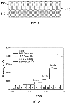
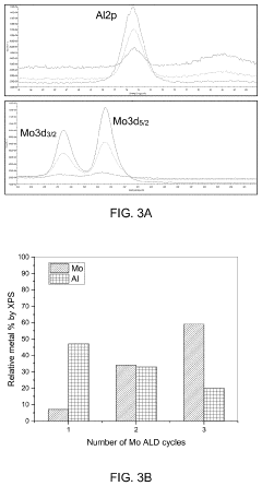
- A method involving atomic layer deposition (ALD) to form ultra-thin transition metal layers, followed by sulphurization, allowing for precise control over the thickness of TMD films, such as MoS2, using a bottom-up approach to overcome the limitations of top-down exfoliation methods.
Transition metal dichalcogenides and uses thereof
PatentWO2021015677A1
Innovation
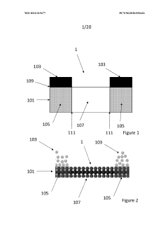
- Surface modification of TMDs with Group 1 metals like Cs and Rb, forming a layer on the surface to achieve a hetero-phase contact between 2H and IT' phases, which reduces contact resistance and enhances electrical properties.
Materials Science Considerations for TMD Implementation
The implementation of transition metal dichalcogenides (TMDs) in straintronics applications requires careful consideration of their material properties and processing requirements. TMDs such as MoS2, WS2, and WSe2 possess unique layered structures that enable exceptional mechanical flexibility while maintaining their electronic properties under strain, making them ideal candidates for strain-engineered electronic devices.
Crystal quality represents a primary consideration for TMD implementation. High-quality single crystals with minimal defects are essential for achieving consistent and predictable strain responses. Defects, grain boundaries, and impurities can significantly alter local strain distributions and create unpredictable variations in electronic properties. Current synthesis methods, including chemical vapor deposition (CVD) and mechanical exfoliation, present different trade-offs between scalability and crystal quality.
Layer thickness control emerges as another critical factor, as the strain response of TMDs varies significantly with the number of layers. Monolayer TMDs typically exhibit the most pronounced bandgap modulation under strain, while multilayer structures demonstrate more complex behaviors due to interlayer interactions. Precise thickness control during fabrication is therefore essential for engineering specific strain-dependent properties.
Substrate selection and interface engineering significantly impact strain transfer efficiency to TMD layers. The ideal substrate should provide strong adhesion to ensure effective strain transfer while minimizing chemical interactions that could alter the TMD's intrinsic properties. Common substrates include flexible polymers (PDMS, PET), which enable dynamic strain application, and rigid substrates (SiO2/Si) for more stable, permanent strain configurations.
Environmental stability presents ongoing challenges for TMD implementation. Many TMDs exhibit sensitivity to oxygen, moisture, and temperature variations, which can degrade their performance over time. Encapsulation strategies using hexagonal boron nitride (h-BN) or atomic layer deposition (ALD) of protective oxides have shown promise in enhancing the long-term stability of strained TMD devices.
Contact engineering remains a significant hurdle for practical device implementation. The formation of low-resistance electrical contacts to strained TMD layers without disrupting the strain state requires careful material selection and deposition techniques. Phase-engineered contacts and edge-contact geometries have demonstrated improved performance compared to traditional metal contacts.
Scalable fabrication methods that maintain precise strain control represent the ultimate challenge for commercial implementation of TMD-based straintronics. Current laboratory demonstrations often rely on manual techniques that are difficult to translate to industrial production. Emerging approaches combining pre-strained substrates with transfer printing or direct growth methods offer promising pathways toward scalable manufacturing of strain-engineered TMD devices.
Scalability and Manufacturing Challenges for Straintronic Devices
The scalability and manufacturing of straintronic devices based on transition metal dichalcogenides (TMDs) present significant challenges that must be addressed before widespread commercial implementation can be achieved. Current laboratory-scale demonstrations of strain engineering in TMDs typically involve manual manipulation or custom-designed experimental setups that are difficult to translate into mass production environments.
One of the primary challenges lies in achieving precise and uniform strain distribution across large-area TMD films. While nanoscale demonstrations have shown promising results, scaling these techniques to wafer-level production introduces inconsistencies in strain profiles, leading to unpredictable variations in bandgap modulation and conductivity control. This variability undermines the reliability required for commercial electronic applications.
The integration of straintronic TMD devices with conventional semiconductor manufacturing processes presents another significant hurdle. Current CMOS fabrication techniques are not optimized for handling the ultrathin, flexible nature of TMD materials, particularly when precise strain control is required. The development of compatible process flows that maintain strain states throughout multiple fabrication steps remains an open challenge.
Material quality and consistency at scale also pose substantial manufacturing barriers. The synthesis of large-area, high-quality TMD films with minimal defects and grain boundaries is essential for uniform strain response. Current growth methods such as chemical vapor deposition (CVD) and molecular beam epitaxy (MBE) struggle to maintain consistent quality beyond laboratory dimensions.
The design and fabrication of strain-inducing structures that can be reliably reproduced in high-volume manufacturing environments represent another critical challenge. Current approaches using flexible substrates, piezoelectric actuators, or microelectromechanical systems (MEMS) often involve complex fabrication steps that are difficult to standardize and scale.
Long-term stability of strain states in TMD-based devices remains largely unexplored. Environmental factors such as temperature fluctuations, humidity, and mechanical vibrations can potentially alter strain profiles over time, affecting device performance and reliability. Developing encapsulation techniques and robust strain-inducing mechanisms that maintain consistent performance throughout device lifetime is essential for commercial viability.
Cost considerations further complicate the manufacturing landscape. Current methods for high-quality TMD synthesis and precise strain engineering involve expensive equipment and time-consuming processes. Transitioning to economically viable manufacturing approaches while maintaining the desired strain control capabilities will require significant innovation in materials processing and device fabrication techniques.
Unlock deeper insights with Patsnap Eureka Quick Research — get a full tech report to explore trends and direct your research. Try now!
Generate Your Research Report Instantly with AI Agent
Supercharge your innovation with Patsnap Eureka AI Agent Platform!
