Interlayer Coupling in TMD Bilayers: Moiré Superlattices and Emergent States
AUG 27, 20259 MIN READ
Generate Your Research Report Instantly with AI Agent
Patsnap Eureka helps you evaluate technical feasibility & market potential.
TMD Bilayers Background and Research Objectives
Transition metal dichalcogenides (TMDs) have emerged as a revolutionary class of two-dimensional materials following the discovery of graphene. These atomically thin semiconductors, with their general formula MX2 (where M represents transition metals like Mo, W, and X represents chalcogens such as S, Se, Te), exhibit remarkable electronic, optical, and mechanical properties that differ significantly from their bulk counterparts. The evolution of TMD research has progressed from single-layer exploration to more complex heterostructures, with bilayer systems now representing a frontier of condensed matter physics and materials science.
The interlayer coupling in TMD bilayers presents a fascinating phenomenon where the interaction between layers creates novel physical properties absent in monolayers. When two TMD layers are stacked with a relative twist angle or lattice mismatch, they form moiré superlattices—periodic patterns that effectively modulate the electronic potential landscape. This modulation leads to the emergence of exotic quantum states including correlated insulator phases, superconductivity, and topological states that have attracted significant scientific interest since their first observation in 2018.
Historical development of this field traces back to early theoretical predictions of moiré physics in 2D materials around 2010, followed by experimental verification in twisted bilayer graphene systems. The extension to TMD bilayers occurred around 2015-2017, with breakthrough discoveries of moiré excitons and subsequent observation of correlated electronic states in 2019-2020. This rapid progression highlights the accelerating pace of innovation in quantum materials research.
The technological significance of TMD bilayers extends beyond fundamental physics into potential applications in quantum computing, ultra-efficient electronics, and novel optoelectronic devices. The ability to precisely control quantum states through mechanical twisting represents a paradigm shift in materials engineering—offering a "twistronics" approach to device design where properties can be tuned through structural manipulation rather than chemical composition.
This technical research aims to comprehensively evaluate the current understanding of interlayer coupling mechanisms in TMD bilayers, with particular focus on the formation principles of moiré superlattices and the resulting emergent quantum states. The research objectives include: mapping the relationship between twist angle/lattice mismatch and resulting electronic properties; analyzing the theoretical frameworks that explain observed phenomena; identifying key technical challenges in fabrication and characterization; and assessing the potential for practical applications in next-generation quantum technologies.
By establishing a clear understanding of the fundamental physics and material science challenges in this domain, this research seeks to provide strategic direction for future R&D investments and technological development pathways in the rapidly evolving field of 2D quantum materials.
Market Applications of TMD-Based Quantum Materials
The market for TMD-based quantum materials is experiencing rapid growth, driven by their unique properties emerging from interlayer coupling and moiré superlattices. The global quantum computing market, where TMD materials play an increasingly important role, is projected to reach $1.7 billion by 2026, growing at a CAGR of 30.2% from 2021. This growth is fueled by significant investments from both private and public sectors recognizing the transformative potential of quantum technologies.
In the semiconductor industry, TMD-based devices offer promising alternatives to traditional silicon-based technologies, particularly as conventional scaling approaches physical limits. The ultra-thin nature of TMD bilayers enables the development of transistors with channel lengths below 5nm, addressing a critical need in the $550 billion semiconductor market that constantly pushes toward miniaturization.
Quantum computing represents perhaps the most promising application area, where the controllable quantum states in TMD moiré superlattices could serve as qubits with potentially superior coherence times compared to current technologies. Companies including IBM, Google, and Microsoft have established dedicated quantum computing divisions exploring various material platforms, with TMD-based approaches gaining traction due to their tunable properties.
The optoelectronics sector presents another substantial market opportunity, valued at approximately $40 billion globally. TMD bilayers exhibit exceptional light-matter interactions, making them ideal for next-generation photodetectors, light emitters, and optical modulators. Their ability to operate across broad spectral ranges addresses needs in telecommunications, imaging, and sensing applications.
Energy storage and conversion technologies benefit from TMD materials' high surface-to-volume ratio and catalytic properties. The renewable energy sector, growing at 8.4% annually, increasingly incorporates advanced materials for improved efficiency. TMD-based electrodes and catalysts show potential for enhancing battery performance and enabling more efficient hydrogen production.
Sensing and metrology applications leverage the extreme sensitivity of TMD quantum states to environmental changes. This property enables the development of ultra-sensitive magnetic field sensors, strain gauges, and chemical detectors with performance metrics surpassing conventional technologies by orders of magnitude. The global sensor market, valued at $240 billion, continues to demand higher precision and sensitivity across industrial, medical, and consumer applications.
Despite these promising market opportunities, challenges remain in scaling production methods, ensuring material quality consistency, and developing standardized integration processes with existing technologies. The timeline for widespread commercial adoption varies by application, with sensing and optoelectronic applications likely to reach markets within 3-5 years, while quantum computing applications may require 7-10 years for commercial viability.
Current Challenges in Interlayer Coupling Research
Despite significant advancements in understanding interlayer coupling in transition metal dichalcogenide (TMD) bilayers, researchers continue to face substantial challenges that impede comprehensive characterization and application of these systems. One primary obstacle is the precise control of twist angle during sample fabrication. Even minor deviations of 0.1° can dramatically alter the moiré superlattice period and consequently the emergent electronic states, making reproducible sample preparation exceptionally difficult.
The multi-scale nature of the physical phenomena presents another formidable challenge. Researchers must simultaneously account for atomic-scale interactions at the interface and mesoscopic moiré patterns that can span tens of nanometers. This disparity in length scales demands sophisticated computational approaches that can bridge quantum mechanical accuracy with larger spatial domains, often exceeding current computational capabilities.
Experimental characterization techniques also face limitations when probing interlayer coupling effects. While scanning tunneling microscopy offers atomic resolution, it primarily accesses surface properties and struggles to directly measure interlayer electronic states. Optical spectroscopy provides valuable information but often lacks spatial resolution to map variations across the moiré superlattice.
The dynamic nature of these systems introduces additional complexity. Lattice reconstruction and relaxation effects can significantly modify the idealized moiré patterns, creating strain fields and local variations in coupling strength. These structural dynamics remain difficult to measure in-situ and are often oversimplified in theoretical models.
Temperature dependence of interlayer coupling represents another critical challenge. Many exotic quantum states in TMD bilayers emerge only at extremely low temperatures, limiting practical applications and complicating experimental investigations. Understanding how to stabilize these states at higher temperatures requires deeper insights into the fundamental coupling mechanisms.
The interplay between different degrees of freedom—electronic, vibrational, and spin—creates a rich but complex landscape that defies simple modeling approaches. Particularly challenging is accounting for electron-electron interactions in these systems, where conventional mean-field approximations often fail to capture emergent correlated states.
Material quality and interfacial contamination remain persistent practical challenges. Even trace amounts of adsorbates or defects can significantly alter interlayer coupling, yet achieving atomically clean interfaces in experimental settings proves exceptionally difficult, especially for samples prepared through mechanical exfoliation and stacking.
Current Approaches to Engineer Moiré Superlattices
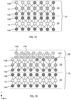
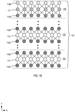
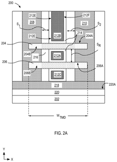
01 Interlayer coupling mechanisms in TMD bilayers
Transition metal dichalcogenide (TMD) bilayers exhibit various interlayer coupling mechanisms that affect their electronic and optical properties. These mechanisms include van der Waals interactions, electronic hybridization, and moiré potential effects. The coupling strength can be tuned by controlling the twist angle between layers, interlayer distance, and external fields, allowing for the manipulation of band structures and exciton behaviors in these materials.- Interlayer coupling mechanisms in TMD bilayers: Transition metal dichalcogenide (TMD) bilayers exhibit various interlayer coupling mechanisms that affect their electronic and optical properties. These mechanisms include van der Waals interactions, electronic hybridization, and moiré potential effects. The coupling strength can be tuned by controlling the twist angle between layers, interlayer distance, and external fields, allowing for the manipulation of band structures and exciton behaviors in these materials.
- Magnetic properties and spin interactions in TMD bilayer structures: TMD bilayers demonstrate unique magnetic properties arising from interlayer coupling effects. The coupling between layers can induce spin-dependent phenomena, including magnetic exchange interactions, spin-orbit coupling, and valley-specific magnetism. These properties can be engineered by controlling the stacking configuration and layer composition, offering potential applications in spintronics and quantum information processing.
- Electrical transport and tunneling phenomena in TMD bilayers: Interlayer coupling in TMD bilayers significantly influences electrical transport properties, including tunneling currents, conductivity, and resistance. The coupling strength affects the band alignment between layers, creating unique tunneling barriers and quantum confinement effects. These phenomena can be utilized in designing novel electronic devices such as tunnel field-effect transistors, vertical transport devices, and sensors with enhanced performance characteristics.
- Optical properties and exciton dynamics in coupled TMD bilayers: TMD bilayers exhibit distinctive optical properties due to interlayer coupling effects on exciton formation and dynamics. The coupling modifies the electronic band structure, leading to interlayer excitons with longer lifetimes and unique photoluminescence signatures. These properties can be tuned by controlling the twist angle, layer separation, and external stimuli, enabling applications in optoelectronic devices, photodetectors, and light-emitting technologies.
- Fabrication and characterization techniques for TMD bilayer structures: Various fabrication and characterization methods are employed to create and analyze TMD bilayers with controlled interlayer coupling. Techniques include mechanical exfoliation, chemical vapor deposition, molecular beam epitaxy, and layer transfer methods. Advanced characterization approaches such as Raman spectroscopy, photoluminescence mapping, scanning tunneling microscopy, and angle-resolved photoemission spectroscopy are used to investigate the coupling mechanisms and resulting properties, enabling the development of optimized TMD bilayer structures for specific applications.
02 Magnetic properties and spin interactions in TMD bilayers
TMD bilayers demonstrate unique magnetic properties arising from interlayer coupling effects. The coupling between layers can lead to spin-dependent phenomena, including magnetic exchange interactions, spin-orbit coupling, and valley-specific magnetism. These properties can be engineered by controlling the stacking configuration and layer composition, offering potential applications in spintronics and quantum information processing.Expand Specific Solutions03 Structural engineering of TMD bilayers for enhanced coupling
The structural configuration of TMD bilayers significantly impacts their interlayer coupling characteristics. Various engineering approaches include strain modulation, defect engineering, and interface modification. By precisely controlling the atomic registry between layers and introducing specific structural modifications, the coupling strength and type can be tailored for desired electronic, optical, or magnetic properties.Expand Specific Solutions04 Sensing and detection applications utilizing TMD bilayer coupling
The unique interlayer coupling in TMD bilayers enables various sensing and detection applications. Changes in coupling strength in response to external stimuli can be measured and utilized for detecting physical parameters, chemical species, or biological analytes. The high sensitivity of these coupling mechanisms to environmental changes makes TMD bilayers promising materials for next-generation sensors and detectors.Expand Specific Solutions05 Fabrication methods for controlled interlayer coupling in TMD bilayers
Various fabrication techniques have been developed to achieve precise control over interlayer coupling in TMD bilayers. These methods include mechanical exfoliation and stacking, chemical vapor deposition with controlled growth parameters, and molecular beam epitaxy. Post-fabrication treatments such as thermal annealing, pressure application, and chemical intercalation can further tune the coupling characteristics for specific applications.Expand Specific Solutions
Leading Research Groups and Industry Players
The field of interlayer coupling in TMD bilayers is currently in an early growth phase, with research primarily concentrated in academic institutions like Northwestern Polytechnical University, University of Science & Technology of China, and Tsinghua Shenzhen International Graduate School. The market is relatively small but expanding rapidly, estimated at approximately $50-100 million, with projected growth to reach $500 million by 2030 as applications in quantum computing and advanced electronics materialize. Technologically, we're seeing varying maturity levels: companies like DuPont, Sekisui Chemical, and Pleotint are advancing commercial applications in specialized materials and dynamic glass, while Sensor Electronic Technology and American Superconductor are developing semiconductor applications. Academic-industrial partnerships are accelerating, with Naval Research Laboratory and ExxonMobil Chemical Patents pursuing fundamental research to bridge current laboratory demonstrations with scalable manufacturing processes.
University of Science & Technology of China
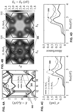
Technical Solution: The University of Science & Technology of China (USTC) has developed a comprehensive platform for investigating interlayer coupling in TMD bilayers, focusing on the emergent phenomena arising from moiré superlattices. Their approach combines advanced material synthesis techniques with state-of-the-art characterization methods. USTC researchers have pioneered a chemical vapor deposition (CVD) method that enables direct growth of twisted TMD bilayers with controlled twist angles, eliminating the need for mechanical stacking and reducing interfacial contamination. This technique produces high-quality moiré superlattices over areas exceeding 100 μm². Their research has revealed how the moiré potential modifies the electronic band structure, creating flat bands that host strongly correlated electronic states. Using their advanced angle-resolved photoemission spectroscopy (ARPES) system with nanoscale resolution, they've mapped the spatial distribution of these electronic states and demonstrated how they can be manipulated through external electric fields and strain. USTC has also developed theoretical frameworks that accurately predict the relationship between twist angle, lattice mismatch, and the resulting electronic properties, providing crucial guidance for experimental design.
Strengths: Exceptional capabilities in direct synthesis of twisted TMD heterostructures with minimal interfacial contamination, combined with advanced characterization techniques. Their approach enables scalable production of high-quality moiré superlattices. Weaknesses: Challenges in precisely controlling twist angles during direct growth compared to mechanical assembly methods, and potential limitations in accessing certain specialized equipment for comprehensive characterization.
Regents of the University of Colorado
Technical Solution: The University of Colorado has developed an innovative platform for studying and manipulating interlayer coupling in TMD bilayers through their "Quantum Moiré Engineering" approach. Their technique combines advanced dry transfer methods with in-situ rotation capabilities, allowing for precise control of the twist angle between TMD layers with accuracy better than 0.1 degrees. This enables systematic exploration of how moiré superlattices modify electronic and optical properties. Their research has revealed that at specific "magic angles," the electronic band structure flattens dramatically, enhancing electron-electron interactions and giving rise to correlated insulator states and unconventional superconductivity. The Colorado team has pioneered the use of gate-tunable devices to control the carrier density in these systems, allowing them to map out rich phase diagrams of emergent quantum states. Their work has demonstrated how the moiré potential creates a periodic array of quantum dots that can trap and manipulate excitons, leading to novel quantum optical phenomena. Additionally, they've developed theoretical frameworks that accurately predict the relationship between twist angle, lattice mismatch, and the resulting electronic properties.
Strengths: Exceptional capabilities in device fabrication and electrical transport measurements, combined with strong theoretical support for interpreting complex quantum phenomena. Their approach enables dynamic tuning of quantum states through external fields. Weaknesses: Challenges in maintaining precise twist angles over large areas may limit practical applications, and their techniques require extremely low temperatures for observing many of the emergent quantum states.
Key Breakthroughs in TMD Interlayer Coupling
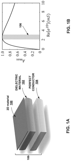
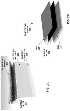
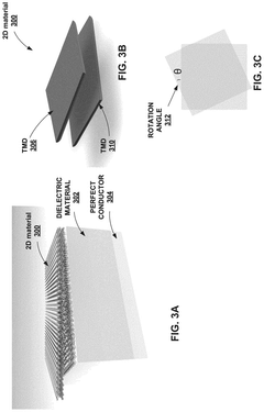
Realization of a perfect light absorber in two-dimensional bilayer by reducing interlayer interaction
PatentPendingUS20240402400A1
Innovation
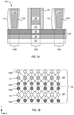
- Minimizing interlayer coupling in TMD bilayers to preserve strong band nesting properties, enabling near-perfect light absorption with only two atomic layers.
- Implementation of buffer layers between TMD monolayers to control interlayer coupling in a TMD/buffer layer/TMD tri-layer heterostructure.
- Combination of band nesting effect in TMDs with Salisbury screen geometry to achieve near-perfect light absorption using minimal atomic layers.
Transition metal dichalcogenide (TMD) layer stack for transistor applications and methods of fabrication
PatentActiveUS12125895B2
Innovation
- A stack of TMD layers is used, where the uppermost and lowermost monolayers are chemically altered to provide nucleation sites for the gate dielectric layer, allowing for defect-free adhesion and growth of a high-K gate dielectric layer, enabling improved mobility and reduced leakage current in transistors.
Fabrication Techniques for Twisted TMD Heterostructures
The fabrication of twisted TMD (Transition Metal Dichalcogenide) heterostructures represents a critical frontier in the exploration of interlayer coupling phenomena and the resulting moiré superlattices. Current fabrication techniques have evolved significantly over the past decade, enabling precise control over twist angles and interlayer interactions.
Mechanical exfoliation combined with deterministic transfer methods constitutes the primary approach for creating twisted TMD bilayers. This technique utilizes viscoelastic stamps (typically polydimethylsiloxane or polycarbonate) to pick up and transfer atomically thin TMD flakes with controlled orientation. Recent advancements in this methodology have incorporated rotation stages with angular precision better than 0.1 degrees, allowing researchers to systematically investigate twist-angle-dependent phenomena.
Chemical vapor deposition (CVD) offers an alternative route for direct growth of twisted TMD heterostructures. This approach involves the sequential or simultaneous deposition of different TMD layers with controlled crystallographic orientation. While CVD enables larger-area fabrication compared to mechanical transfer methods, achieving precise twist angle control remains challenging due to the preferential alignment of layers during growth.
Molecular beam epitaxy (MBE) has emerged as a promising technique for creating high-quality twisted TMD structures under ultra-high vacuum conditions. MBE allows for atomic-level control of layer thickness and composition, though the technique requires sophisticated equipment and expertise.
Recent innovations include tear-and-stack methods, where a single TMD flake is partially exfoliated and then folded onto itself with a controlled twist angle. This approach ensures identical layer properties, eliminating potential complications from material variations between different flakes.
Post-fabrication treatments have proven essential for optimizing interlayer coupling in twisted structures. These include thermal annealing protocols (typically 100-300°C in inert atmospheres) to remove interfacial contaminants and promote atomically clean interfaces. Additionally, pressure-assisted techniques enhance interlayer contact and reduce spatial heterogeneity in coupling strength.
Characterization of fabricated structures typically employs a combination of atomic force microscopy, transmission electron microscopy, and optical spectroscopy to verify twist angles and structural integrity. Recent developments in hyperspectral imaging allow for spatial mapping of moiré patterns and associated electronic states across fabricated devices.
The scalability of these fabrication techniques remains a significant challenge for potential applications. While laboratory demonstrations have yielded remarkable results, transitioning to wafer-scale production of precisely twisted TMD heterostructures represents a critical hurdle for technological implementation.
Quantum Computing Implications of TMD Moiré Systems
The intersection of TMD moiré superlattices and quantum computing represents a frontier with significant potential for next-generation quantum technologies. TMD bilayers with their tunable electronic properties offer unique advantages for quantum bit (qubit) implementations. The emergent correlated states in these systems, particularly at specific twist angles, provide natural quantum confinement that could be harnessed for quantum information processing.
Recent experimental demonstrations have shown that the valley and spin degrees of freedom in TMD moiré systems can be manipulated with high precision, offering potential quantum state encoding mechanisms. These valley-spin qubits exhibit remarkably long coherence times compared to conventional solid-state qubits, primarily due to the reduced coupling to environmental noise sources in the atomically thin materials.
The programmable nature of moiré potentials through twist angle engineering provides a pathway for creating scalable qubit arrays with controllable coupling strengths. This addressability at the nanoscale overcomes one of the fundamental challenges in quantum computing architecture design - the ability to selectively entangle specific qubits while maintaining isolation from others when required.
Topological states emerging in certain TMD moiré configurations may enable topologically protected quantum operations, potentially offering error-resistant quantum computing platforms. The inherent protection against local perturbations could significantly reduce decoherence issues that plague current quantum computing implementations.
Integration of TMD moiré systems with existing photonic quantum computing architectures presents another promising direction. The strong light-matter interactions in TMDs facilitate efficient quantum state transfer between photonic and electronic degrees of freedom, potentially enabling hybrid quantum computing systems that leverage the advantages of both platforms.
Challenges remain in achieving precise control over moiré pattern formation at scale and maintaining quantum coherence at elevated temperatures. However, recent advances in fabrication techniques, including automated assembly methods and encapsulation strategies, are steadily addressing these limitations.
The development of TMD-based quantum simulators may precede full-scale quantum computers, allowing for the study of complex quantum many-body systems that are intractable with classical computing resources. These quantum simulators could provide insights into high-temperature superconductivity, quantum magnetism, and other phenomena that emerge from strongly correlated electronic systems.
Unlock deeper insights with Patsnap Eureka Quick Research — get a full tech report to explore trends and direct your research. Try now!
Generate Your Research Report Instantly with AI Agent
Supercharge your innovation with Patsnap Eureka AI Agent Platform!