Optical Properties of TMDs: Excitons, Trions, and Polaritons
AUG 27, 20259 MIN READ
Generate Your Research Report Instantly with AI Agent
Patsnap Eureka helps you evaluate technical feasibility & market potential.
TMDs Optical Properties Background and Research Objectives
Transition metal dichalcogenides (TMDs) have emerged as a revolutionary class of two-dimensional materials following the discovery of graphene. Since 2010, these atomically thin semiconductors have garnered significant attention due to their exceptional optical properties, which differ dramatically from their bulk counterparts. The transition from indirect bandgap in bulk form to direct bandgap in monolayer configuration has positioned TMDs as promising candidates for next-generation optoelectronic applications.
The optical behavior of TMDs is dominated by strong excitonic effects resulting from reduced dielectric screening and enhanced Coulomb interactions in the two-dimensional limit. These materials exhibit binding energies of several hundred meV, allowing excitons to persist even at room temperature—a stark contrast to conventional semiconductors where excitons typically require cryogenic conditions to observe.
Historical development of TMD optical research shows three distinct phases: initial discovery and characterization (2010-2014), advanced spectroscopic investigations (2015-2018), and application-oriented research (2019-present). The field has evolved from fundamental studies of basic optical properties to sophisticated manipulation of quantum optical phenomena for technological applications.
The unique band structure of TMDs gives rise to valley-selective optical excitation, where circularly polarized light can selectively populate K or K' valleys in the Brillouin zone. This valley degree of freedom represents a new quantum property that can potentially be harnessed for information processing, establishing the foundation for "valleytronics."
Beyond neutral excitons, TMDs host a rich landscape of excitonic complexes including charged excitons (trions), biexcitons, and dark excitons. More recently, strong light-matter coupling in TMD-based optical cavities has enabled the formation of polaritons—hybrid light-matter quasiparticles with unique coherence properties and nonlinear behaviors.
The primary research objectives in this field include: (1) developing comprehensive understanding of exciton dynamics and interactions in various TMD compositions; (2) establishing reliable methods for controlling and manipulating excitonic properties through external stimuli such as electric fields, strain, and heterostructure engineering; (3) exploring quantum optical phenomena for quantum information applications; and (4) advancing practical implementations of TMD-based optoelectronic devices including light-emitting diodes, photodetectors, and lasers.
Current technological limitations center around material quality, scalable fabrication methods, and environmental stability. Addressing these challenges requires interdisciplinary approaches combining materials science, quantum physics, and device engineering to fully realize the potential of TMDs in next-generation optical technologies.
Market Applications and Demand for TMD-based Optoelectronics
The global market for TMD-based optoelectronic devices is experiencing significant growth, driven by the unique optical properties of transition metal dichalcogenides (TMDs). Industry analysts project the broader 2D materials market, which includes TMDs, to reach approximately $12 billion by 2027, with optoelectronic applications representing a substantial segment of this market.
The demand for TMD-based optoelectronics is primarily fueled by the telecommunications and data transmission sectors, where the exceptional light-matter interaction capabilities of TMDs offer solutions for next-generation photonic integrated circuits. The ability of TMDs to host stable excitons at room temperature provides a competitive advantage over traditional semiconductor materials in optical switching and modulation applications.
Consumer electronics represents another major market driver, with smartphone manufacturers exploring TMD-based photodetectors and light emitters for improved display technologies and sensing capabilities. The atomically thin nature of TMDs allows for flexible, transparent, and ultra-compact optoelectronic components that align with the industry trend toward thinner and more versatile devices.
The quantum information processing sector has emerged as a high-value niche market for TMD-based optoelectronics. The valley-selective optical properties of excitons and trions in TMDs offer promising platforms for quantum bit operations and single-photon emission, attracting substantial research funding from both government agencies and private technology companies.
Energy harvesting applications represent a growing market segment, with TMD-based photovoltaics showing potential for enhanced light absorption efficiency. The tunable bandgap of various TMD materials allows for customized solar spectrum targeting, which is particularly valuable for specialized applications in aerospace and remote sensing.
Medical diagnostics and biosensing markets are increasingly exploring TMD-based optical sensors, leveraging the strong exciton-based photoluminescence for enhanced sensitivity in biomarker detection. The healthcare sector's demand for point-of-care diagnostic tools is creating new opportunities for TMD-based optoelectronic biosensors with improved performance metrics.
Despite the promising market outlook, industry adoption faces challenges related to manufacturing scalability and device stability. Current market penetration remains limited to high-value applications where performance advantages outweigh cost considerations. The transition from laboratory demonstrations to commercial products requires further advances in large-area synthesis techniques and encapsulation methods to protect the sensitive optical properties of TMDs from environmental degradation.
Current State and Challenges in TMDs Exciton Research
The field of transition metal dichalcogenides (TMDs) exciton research has witnessed remarkable progress globally, with significant advancements in understanding the fundamental properties and potential applications of these two-dimensional materials. Currently, researchers have established that TMDs exhibit strong excitonic effects due to reduced dielectric screening and quantum confinement, resulting in binding energies of hundreds of meV—orders of magnitude larger than those in conventional semiconductors.
Despite these advances, several critical challenges persist in TMDs exciton research. The primary technical obstacle involves controlling and manipulating exciton dynamics with precision. Excitons in TMDs are highly sensitive to environmental factors, substrate interactions, and defects, making reproducible experiments challenging. The valley-specific optical selection rules, while promising for valleytronics applications, remain difficult to exploit reliably due to rapid valley depolarization at elevated temperatures.
Another significant challenge lies in the scalable production of high-quality, defect-free TMD monolayers. Current synthesis methods, including chemical vapor deposition (CVD) and mechanical exfoliation, often produce samples with varying quality and inconsistent optical properties. This variability directly impacts exciton behavior and hampers progress toward practical applications.
The characterization of trion and biexciton states presents additional complexities. These many-body states, critical for understanding the full optical response of TMDs, require sophisticated spectroscopic techniques and theoretical models to accurately identify and analyze. The interplay between excitons, trions, and the underlying electronic structure remains incompletely understood, particularly under varying external conditions such as strain, electric fields, and magnetic fields.
Geographically, TMD exciton research exhibits distinct regional strengths. North American institutions lead in fundamental spectroscopic studies and theoretical modeling, while East Asian research groups, particularly in China, South Korea, and Japan, demonstrate excellence in material synthesis and device fabrication. European teams have made significant contributions to valley physics and polariton studies in TMDs.
The integration of TMD excitons with photonic structures to form polaritons represents a frontier area with substantial challenges. While strong light-matter coupling has been demonstrated in various configurations, achieving room-temperature polariton condensation and developing practical polariton-based devices remain elusive goals. The ultrafast dynamics of these hybrid light-matter states require advanced measurement techniques that push the boundaries of current spectroscopic capabilities.
Existing Methodologies for TMDs Optical Characterization
01 Exciton properties in TMD materials
Transition Metal Dichalcogenides (TMDs) exhibit strong excitonic effects due to reduced dielectric screening and quantum confinement in their 2D structure. These materials show large binding energies for excitons, making them stable even at room temperature. The exciton properties can be tuned by controlling layer thickness, strain, and substrate interactions, which affects the optical absorption and emission characteristics. These unique excitonic properties make TMDs promising for optoelectronic applications.- Exciton properties in TMD materials: Transition Metal Dichalcogenides (TMDs) exhibit strong excitonic effects due to reduced dielectric screening and quantum confinement in their 2D structure. These materials show large binding energies for excitons, making them stable even at room temperature. The exciton properties can be tuned by controlling layer thickness, strain, and substrate interactions, which affects the optical absorption and emission characteristics of TMDs. These unique excitonic properties make TMDs promising for optoelectronic applications.
- Trion formation and manipulation in TMDs: Trions (charged excitons) form in TMDs when an exciton binds with an additional electron or hole. These quasi-particles significantly influence the optical properties of TMDs and can be controlled through electrical gating or doping. Trions in TMDs exhibit distinct spectral features and longer lifetimes compared to neutral excitons. The ability to manipulate trion formation provides an additional degree of freedom for controlling the optical response of TMD-based devices, enabling applications in quantum information processing and optoelectronics.
- Polariton phenomena in TMD structures: When TMDs are integrated with optical cavities or plasmonic structures, strong light-matter coupling can lead to the formation of polaritons - hybrid quasi-particles combining properties of photons and excitons. These TMD-based polaritons exhibit unique dispersion relations and can enable room-temperature polariton condensation. The strong coupling regime in TMDs allows for manipulation of light propagation and emission characteristics, opening pathways for novel photonic devices including low-threshold lasers and optical switches.
- Valley-dependent optical properties of TMDs: TMDs possess valley-dependent optical selection rules, where circularly polarized light can selectively excite carriers in specific valleys (K or K') of the Brillouin zone. This valley-selective excitation enables valley polarization and coherence, which can be utilized for valleytronic applications. The valley degree of freedom in TMDs provides an additional channel for information processing and storage. The interplay between spin and valley physics in TMDs leads to unique optical phenomena that can be exploited for quantum information technologies.
- Engineering TMD heterostructures for enhanced optical properties: Vertical stacking of different TMD materials creates heterostructures with tailored optical properties. These heterostructures can exhibit type-I or type-II band alignment, leading to interlayer excitons with long lifetimes and enhanced light-matter interactions. By controlling the twist angle between layers, moiré patterns form, creating periodic potential landscapes that modify the optical properties. TMD heterostructures enable precise engineering of exciton binding energies, optical bandgaps, and quantum emission characteristics, advancing applications in photonics, quantum light sources, and photodetectors.
02 Trion formation and manipulation in TMDs
Trions (charged excitons) in TMDs form when an exciton binds with an additional electron or hole. These quasi-particles exhibit distinct optical signatures that can be controlled through electrical gating or doping. The trion binding energy in TMDs is significantly larger than in conventional semiconductors, allowing for their observation at higher temperatures. The ability to manipulate trion formation provides additional control over the optical properties of TMD-based devices and enables novel optoelectronic functionalities.Expand Specific Solutions03 Polariton phenomena in TMD structures
When TMDs are integrated with optical cavities or plasmonic structures, strong light-matter coupling can lead to the formation of polaritons - hybrid quasi-particles combining properties of photons and excitons. These TMD-based polaritons exhibit unique dispersion characteristics and can enable novel optical phenomena such as Bose-Einstein condensation at elevated temperatures. The polariton properties can be engineered by controlling the cavity design and TMD layer configuration, offering pathways for developing novel photonic devices.Expand Specific Solutions04 Valley-dependent optical properties of TMDs
TMDs possess valley-dependent optical selection rules, where circularly polarized light can selectively excite carriers in specific valleys (K or K') in momentum space. This valley-selective excitation enables the generation and detection of valley polarization and coherence through optical means. The valley degree of freedom provides an additional control parameter for information processing and can be manipulated through external fields. These valley-dependent optical properties make TMDs promising candidates for valleytronics applications.Expand Specific Solutions05 Heterostructure engineering for enhanced optical properties
Vertical stacking of different TMD materials creates van der Waals heterostructures with tunable optical properties. These heterostructures can exhibit type-II band alignment, facilitating spatial separation of electrons and holes across different layers. This separation leads to the formation of interlayer excitons with longer lifetimes and unique optical signatures. By engineering the layer composition and stacking sequence, the optical properties can be precisely controlled, enabling the development of novel light-emitting and light-harvesting devices with enhanced performance.Expand Specific Solutions
Leading Research Groups and Companies in TMDs Development
The field of "Optical Properties of TMDs: Excitons, Trions, and Polaritons" is currently in a growth phase, with increasing research interest but still evolving commercial applications. The global market for TMD-based optoelectronics is expanding, projected to reach significant value as these materials find applications in next-generation displays, sensors, and quantum technologies. Leading academic institutions like Peking University and University of Southern California are advancing fundamental research, while companies including Universal Display Corporation, BOE Technology, and Sharp are exploring commercial implementations. Research organizations such as Japan Science & Technology Agency and Institute for Basic Science provide critical infrastructure support. The technology remains in early-to-mid maturity, with significant R&D investment from both academic and industrial players working to overcome challenges in scalability and integration.
Changchun Institute of Applied Chemistry, Chinese Academy of Sciences
Technical Solution: Changchun Institute of Applied Chemistry (CIAC) has developed innovative approaches to studying and manipulating the optical properties of TMDs. Their research program combines advanced material synthesis techniques with sophisticated optical characterization methods. CIAC researchers have pioneered chemical vapor deposition methods for growing high-quality monolayer TMDs with controlled defect densities, allowing systematic studies of how defects influence exciton dynamics. They've developed spectroscopic techniques to investigate the formation and recombination of trions in TMDs under various doping conditions, revealing how carrier concentration affects optical properties. Their work on TMD-based heterostructures has demonstrated interlayer excitons with prolonged lifetimes and unique spin-valley locking characteristics[11]. In the field of polaritonics, CIAC has created hybrid TMD-plasmonic nanostructures that achieve strong coupling between excitons and surface plasmons, leading to enhanced light-matter interactions and modified emission properties. A significant contribution has been their development of chemical functionalization methods to tune the optical properties of TMDs post-synthesis, providing an additional degree of freedom for engineering exciton energies and dynamics[12]. Recent work includes investigating the role of substrate interactions on exciton diffusion and valley depolarization in monolayer TMDs.
Strengths: Exceptional capabilities in chemical synthesis and functionalization of TMDs, allowing precise control over material properties. Strong integration of materials chemistry with optical physics for novel hybrid structures. Weaknesses: Some of their chemical modification approaches may introduce additional defects or inhomogeneities that complicate device integration. Their focus on fundamental material properties sometimes delays translation to practical applications.
Peking University
Technical Solution: Peking University has established a comprehensive research program on TMD optical properties, particularly focusing on the manipulation of valley excitons and trions. Their researchers have developed innovative approaches to control valley polarization through external fields, including electrical, magnetic, and strain engineering. They've demonstrated the ability to tune exciton binding energies and valley splitting in monolayer TMDs through electrostatic gating techniques. A significant contribution is their work on moiré excitons in twisted TMD heterostructures, where they've observed novel quantum confined states with distinct optical signatures[2]. Their research extends to polariton physics, where they've created TMD-based microcavities that achieve strong coupling between excitons and photons, leading to polariton condensation at elevated temperatures. Recent publications highlight their success in fabricating high-quality van der Waals heterostructures that preserve intrinsic exciton properties while enabling precise control over interlayer interactions, advancing both fundamental understanding and potential applications in quantum information processing[4][7].
Strengths: Exceptional capabilities in fabricating high-quality TMD samples and heterostructures with precise control over layer number and stacking orientation. Strong integration of theoretical modeling with experimental results. Weaknesses: Some of their most advanced techniques require extremely low temperatures (< 10K) for observation of quantum effects, limiting practical applications. Their focus on fundamental physics may delay translation to commercial technologies.
Key Breakthroughs in Exciton, Trion and Polariton Physics
Methods of Tailoring The Optical Properties of Transition Metal Dichalcogenides
PatentInactiveUS20220212947A1
Innovation
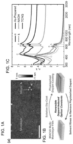
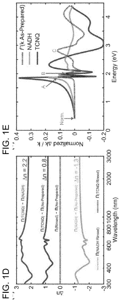
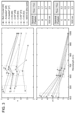
- The introduction of organic or inorganic chemical dopants, such as nicotinamide adenine dinucleotide (NADH) and 7,7,8,8-tetracyanoquinodimethane (TCNQ), through physisorbed interactions, allows for reversible changes in the refractive index and extinction coefficient of transition metal dichalcogenides, such as MoS2, by varying the dielectric polarizability and charge transfer effects, enabling broad modulation of optical constants.
Materials Integration and Fabrication Techniques
The integration of transition metal dichalcogenides (TMDs) into functional devices for exploiting their unique optical properties requires sophisticated fabrication techniques. Mechanical exfoliation remains the gold standard for obtaining high-quality TMD monolayers with superior optical properties, enabling the observation of sharp exciton resonances and valley-specific phenomena. However, this method faces scalability challenges for industrial applications.
Chemical vapor deposition (CVD) has emerged as a promising approach for large-scale TMD synthesis, allowing controlled growth of monolayers with reasonable optical quality. Recent advancements in CVD techniques have significantly improved the crystallinity and reduced defect densities, enhancing exciton lifetimes and quantum yields. Metal-organic chemical vapor deposition (MOCVD) further refines this process, offering precise control over layer thickness and composition, critical for engineering specific exciton-polariton interactions.
Molecular beam epitaxy (MBE) provides another avenue for high-quality TMD growth, particularly valuable for creating heterostructures with atomically sharp interfaces. These interfaces are crucial for interlayer excitons and novel polariton physics. The ultra-high vacuum conditions in MBE minimize contamination, preserving the intrinsic optical properties of TMDs.
For polariton studies, integration of TMDs with optical cavities presents unique fabrication challenges. Techniques such as transfer printing and deterministic stamping have been developed to precisely position TMD monolayers within photonic crystal cavities or between distributed Bragg reflectors. The cavity quality factor and coupling strength must be carefully engineered to achieve strong coupling regimes where polaritons form.
Encapsulation methods using hexagonal boron nitride (h-BN) have revolutionized TMD device fabrication, creating "sandwich structures" that protect TMDs from environmental degradation. These structures dramatically enhance optical properties by reducing inhomogeneous broadening and increasing exciton and trion stability. The atomically flat h-BN surfaces minimize substrate-induced disorder, allowing observation of narrow linewidth optical transitions.
Advanced lithography and etching techniques enable the creation of TMD-based photonic structures like waveguides and resonators, facilitating directional polariton propagation and confinement. Complementary techniques such as focused ion beam milling and electron beam lithography provide nanometer-scale precision for creating deterministic defects that can act as single-photon emitters or localization sites for trions.
Quantum Information Applications of TMD Optical Properties
The unique optical properties of transition metal dichalcogenides (TMDs) present significant opportunities for quantum information applications. The strong light-matter interactions, valley-specific optical selection rules, and long-lived coherence times make TMDs particularly attractive for quantum computing, communication, and sensing platforms.
Excitons in TMDs can serve as quantum bits (qubits) due to their discrete energy levels and controllable quantum states. The valley degree of freedom offers an additional quantum information carrier, enabling valley qubits that can be optically initialized, manipulated, and read out. This valley pseudospin represents a promising quantum information resource that is uniquely accessible in TMD materials.
Trions, as charged exciton complexes, provide another avenue for quantum information processing. Their spin-valley configurations can encode quantum information with enhanced stability compared to neutral excitons. The electrical control of trion formation enables switching between different quantum states, facilitating quantum gate operations essential for quantum computing architectures.
Polaritons in TMD-based optical cavities demonstrate strong coupling regimes that can be leveraged for quantum simulation and quantum nonlinear optics. These hybrid light-matter quasiparticles exhibit quantum correlations and entanglement properties that are fundamental for quantum information protocols. The ability to engineer polariton interactions through cavity design offers a versatile platform for implementing quantum algorithms.
Recent experimental demonstrations have shown quantum emission from localized defects in TMDs, producing single photons with high purity and indistinguishability. These quantum light sources are essential building blocks for photonic quantum networks and secure quantum communication systems based on quantum key distribution protocols.
The integration of TMD-based quantum emitters with nanophotonic structures has enabled enhanced light extraction efficiency and directional emission control. This advancement addresses a critical challenge in quantum communication—efficiently interfacing flying qubits (photons) with stationary qubits (excitons or trions).
Quantum memories based on TMD optical properties have also been developed, utilizing the long valley coherence times to store quantum information. These memories are crucial components for quantum repeaters in long-distance quantum communication networks, potentially overcoming current distance limitations in quantum key distribution systems.
Looking forward, the scalability of TMD-based quantum information systems presents both opportunities and challenges. The potential for wafer-scale fabrication of TMD devices offers advantages over other quantum platforms, while maintaining operation at more accessible temperatures compared to superconducting or trapped-ion systems.
Unlock deeper insights with Patsnap Eureka Quick Research — get a full tech report to explore trends and direct your research. Try now!
Generate Your Research Report Instantly with AI Agent
Supercharge your innovation with Patsnap Eureka AI Agent Platform!