How to Engineer Edge States in TMD Nanoribbons
AUG 27, 20259 MIN READ
Generate Your Research Report Instantly with AI Agent
Patsnap Eureka helps you evaluate technical feasibility & market potential.
TMD Nanoribbon Edge States Background and Objectives
Transition metal dichalcogenides (TMDs) have emerged as a revolutionary class of two-dimensional materials following the discovery of graphene. These atomically thin semiconductors, with their unique electronic, optical, and mechanical properties, have attracted significant attention in the scientific community over the past decade. When TMDs are confined into quasi-one-dimensional structures known as nanoribbons, they exhibit fascinating edge-dependent properties that dramatically alter their electronic behavior.
The evolution of TMD nanoribbon research has progressed from initial theoretical predictions to experimental realizations. Early computational studies in the 2010s predicted that zigzag-edged MoS2 nanoribbons would exhibit metallic edge states, while armchair-edged variants would maintain semiconducting properties. This edge-dependent behavior represents a fundamental departure from the properties of their bulk counterparts and offers unprecedented opportunities for electronic applications.
The engineering of edge states in TMD nanoribbons aims to achieve precise control over electronic properties through edge structure manipulation. This includes controlling edge termination (zigzag, armchair, or mixed), edge functionalization with various chemical groups, and strain engineering. The ultimate goal is to develop methods for deterministic creation of specific edge configurations that yield desired electronic properties for applications in nanoelectronics, spintronics, and quantum computing.
Recent advances in synthesis techniques, including bottom-up chemical approaches and top-down lithographic methods, have enabled more precise fabrication of TMD nanoribbons with controlled edge structures. However, significant challenges remain in achieving atomic-level precision and scalability in production. The field is now moving toward developing reliable methods for edge engineering that can be implemented at industrial scales.
The technological trajectory of TMD nanoribbon edge engineering intersects with broader trends in nanomaterials and quantum technologies. As quantum computing and spintronics continue to advance, the ability to manipulate edge states becomes increasingly valuable for creating novel quantum devices. Additionally, the unique electronic properties of engineered edge states could enable ultra-low power electronics that address energy efficiency challenges in computing.
Understanding and controlling edge states in TMD nanoribbons represents a critical frontier in nanomaterial science with far-reaching implications for next-generation electronics. This technical exploration aims to comprehensively assess the current state of knowledge, identify key challenges, and outline promising research directions for engineering edge states in TMD nanoribbons to unlock their full technological potential.
Market Applications for Engineered TMD Edge States
The engineered edge states in TMD nanoribbons present significant market opportunities across multiple industries due to their unique electronic, optical, and magnetic properties. The semiconductor industry stands to benefit substantially from these materials, as they offer potential solutions for next-generation transistors with reduced power consumption and enhanced performance. TMD edge states could enable the development of ultra-thin field-effect transistors that overcome silicon's scaling limitations, addressing the growing demand for more efficient computing devices.
In the energy sector, TMD nanoribbons with engineered edge states show promise for catalytic applications, particularly in hydrogen evolution reactions and other energy conversion processes. Their high edge-to-surface ratio and tunable electronic properties make them attractive alternatives to traditional noble metal catalysts, potentially reducing costs while maintaining or improving efficiency in fuel cells and electrolyzers.
Quantum computing represents another high-value application area. The topologically protected edge states in certain TMD configurations could serve as robust quantum bits (qubits), less susceptible to environmental decoherence than conventional approaches. This characteristic addresses one of the fundamental challenges in quantum computing development, potentially accelerating the commercialization timeline for practical quantum systems.
Sensor technologies benefit from the high sensitivity of TMD edge states to environmental changes. Gas sensors, biosensors, and chemical detectors utilizing these materials demonstrate superior detection limits and selectivity compared to conventional sensing platforms. The healthcare and environmental monitoring sectors could leverage these advantages for point-of-care diagnostics and pollution detection systems.
Optoelectronic applications constitute another promising market segment. The direct bandgap nature of many TMDs, combined with engineered edge states, enables efficient light emission and absorption. This property supports the development of next-generation displays, photodetectors, and optical communication devices with enhanced performance characteristics and reduced power requirements.
Defense and aerospace industries are exploring TMD edge states for radiation-hardened electronics and specialized sensing applications. The inherent stability of certain TMD configurations in extreme environments makes them suitable for mission-critical systems where conventional semiconductor technologies face limitations.
The emerging spintronics market represents perhaps the most transformative long-term application. TMD edge states can host spin-polarized currents, enabling novel memory and logic devices that operate on spin rather than charge. This approach could dramatically reduce power consumption while increasing processing capabilities in future computing architectures.
Current Challenges in TMD Nanoribbon Engineering
Despite significant advancements in TMD nanoribbon research, several critical challenges continue to impede progress in effectively engineering edge states. The primary obstacle remains the precise fabrication of nanoribbons with atomically clean and well-defined edges. Current top-down approaches, including lithography and etching techniques, often introduce defects and contamination at the edges, significantly altering the electronic properties and undermining the theoretical predictions of edge states.
The controlled synthesis of zigzag versus armchair edge configurations presents another substantial challenge. Theoretical studies consistently demonstrate that zigzag edges host more robust and technologically valuable edge states compared to armchair configurations, yet selectively producing zigzag edges with high fidelity remains elusive in practical synthesis methods.
Environmental stability poses a significant hurdle, as edge states in TMD nanoribbons exhibit extreme sensitivity to ambient conditions. Oxygen, water vapor, and other atmospheric components readily interact with the dangling bonds at nanoribbon edges, causing degradation of the desired electronic properties. This necessitates either sophisticated encapsulation strategies or ultra-high vacuum environments for both fabrication and characterization.
Characterization limitations further complicate progress, as conventional techniques struggle to provide atomic-resolution information about edge structures and associated electronic states simultaneously. While scanning tunneling microscopy offers excellent spatial resolution, it requires specialized sample preparation and cannot easily be integrated with device fabrication workflows.
Scale-up and integration challenges represent perhaps the most significant barrier to practical applications. Current methods capable of producing high-quality edge states typically yield only small quantities of nanoribbons or isolated structures that are difficult to position and integrate into functional devices or circuits.
The theoretical-experimental gap remains problematic, with computational predictions often failing to account for real-world complexities such as substrate interactions, strain effects, and partial edge reconstructions. This discrepancy between idealized models and experimental realities hinders the development of reliable design principles for edge state engineering.
Lastly, the challenge of tuning and controlling edge states post-fabrication limits their practical utility. While theoretical work suggests possibilities for dynamic manipulation of edge states through external fields or chemical functionalization, implementing these approaches without disrupting the fragile edge states remains technically demanding.
Current Methodologies for Edge State Engineering
01 Electronic properties of TMD nanoribbon edge states
Transition metal dichalcogenide (TMD) nanoribbons exhibit unique electronic properties at their edges, including metallic edge states that can be tuned for various applications. These edge states show distinct quantum confinement effects and can display different electronic behaviors compared to the bulk material. The electronic structure of these edge states can be engineered by controlling the width, edge termination, and composition of the nanoribbons, making them promising for next-generation electronic devices.- Electronic properties of TMD nanoribbon edge states: Transition metal dichalcogenide (TMD) nanoribbons exhibit unique electronic properties at their edges, including metallic edge states that can be tuned for various applications. These edge states show distinct quantum behaviors such as spin-polarization and topological properties that differ from the bulk material. The electronic structure of these edge states can be engineered by controlling the width, edge termination, and composition of the nanoribbons, making them promising for next-generation electronic devices.
- Fabrication methods for TMD nanoribbons with controlled edge states: Various fabrication techniques have been developed to create TMD nanoribbons with well-defined edge states. These methods include lithographic patterning, chemical etching, bottom-up synthesis, and mechanical exfoliation. Each approach offers different levels of control over the edge structure, which is crucial for determining the electronic properties of the edge states. Advanced techniques allow for atomic precision in creating zigzag or armchair edges, which exhibit different electronic behaviors.
- Applications of TMD nanoribbon edge states in electronic devices: The unique properties of TMD nanoribbon edge states make them suitable for various electronic applications. These include field-effect transistors with enhanced carrier mobility, spintronic devices that utilize the spin-polarized nature of edge states, and quantum computing components. The metallic character of certain edge configurations enables their use as interconnects in nanoelectronic circuits, while their sensitivity to the local environment makes them excellent candidates for sensing applications.
- Modification and functionalization of TMD nanoribbon edges: The edge states of TMD nanoribbons can be modified through various functionalization strategies to tailor their properties. Chemical functionalization with different atomic species or molecular groups can alter the electronic structure of edge states. Strain engineering, defect introduction, and heterostructure formation are additional approaches to manipulate edge state properties. These modifications enable fine-tuning of bandgaps, magnetic properties, and conductivity at the edges.
- Characterization techniques for TMD nanoribbon edge states: Advanced characterization methods are essential for studying the properties of TMD nanoribbon edge states. Scanning tunneling microscopy/spectroscopy (STM/STS) provides atomic-resolution imaging and local electronic structure information. Transport measurements reveal the conductive properties of edge states, while optical spectroscopy techniques can probe their energy levels. Theoretical modeling and computational methods complement experimental approaches by predicting edge state behaviors and guiding experimental design.
02 Fabrication methods for TMD nanoribbons with controlled edge states
Various fabrication techniques have been developed to create TMD nanoribbons with well-defined edge states. These methods include lithographic patterning, chemical etching, bottom-up synthesis, and mechanical exfoliation. Each technique offers different levels of control over the edge structure, which is crucial for determining the electronic properties of the edge states. Advanced fabrication methods focus on creating atomically precise edges to achieve consistent electronic performance in devices based on TMD nanoribbon edge states.Expand Specific Solutions03 Applications of TMD nanoribbon edge states in electronic devices
The unique electronic properties of TMD nanoribbon edge states make them suitable for various electronic applications. These include field-effect transistors with enhanced carrier mobility, spintronic devices that utilize the spin-polarized nature of certain edge states, and quantum computing components. The metallic character of edge states in semiconducting TMD nanoribbons can be exploited to create novel device architectures with improved performance characteristics compared to conventional semiconductor devices.Expand Specific Solutions04 Modification and functionalization of TMD nanoribbon edges
The edge states of TMD nanoribbons can be modified through various functionalization techniques to tailor their properties for specific applications. These modifications include passivation with different chemical groups, doping with heteroatoms, and creation of heterostructures. Such functionalization can alter the electronic structure, stability, and reactivity of the edge states, enabling the development of sensors, catalysts, and other functional materials based on TMD nanoribbons.Expand Specific Solutions05 Theoretical modeling and characterization of TMD nanoribbon edge states
Advanced theoretical and experimental techniques are employed to understand and characterize the edge states in TMD nanoribbons. Computational methods such as density functional theory (DFT) and tight-binding models help predict the electronic structure of edge states under various conditions. Experimental characterization techniques include scanning tunneling microscopy (STM), angle-resolved photoemission spectroscopy (ARPES), and transport measurements. These approaches provide insights into the fundamental physics of edge states and guide the development of TMD nanoribbon-based technologies.Expand Specific Solutions
Leading Research Groups and Industry Players in TMD Technology
The engineering of edge states in TMD nanoribbons is currently in an early growth phase, with the market expanding as research transitions toward commercial applications. The global market for TMD-based nanoelectronics is projected to reach significant scale as quantum computing and advanced electronics industries mature. Technologically, the field shows promising but varied maturity levels across different players. Research institutions like University of Electronic Science & Technology of China and King Abdullah University of Science & Technology are pioneering fundamental research, while industry leaders including IBM, Intel, and TSMC are developing practical applications. GlobalFoundries and Taiwan Semiconductor are advancing fabrication techniques, with specialized companies like United Monolithic Semiconductors focusing on niche implementations for next-generation electronic devices.
International Business Machines Corp.
Technical Solution: IBM has developed a comprehensive approach to engineering edge states in transition metal dichalcogenide (TMD) nanoribbons through their advanced nanofabrication techniques. Their method involves precise lithographic patterning combined with controlled etching processes to create zigzag-edged MoS2 nanoribbons with widths down to 10nm. IBM researchers have demonstrated that these engineered edge states exhibit magnetic properties that can be tuned by applying external electric fields, making them promising for spintronic applications. The company has also pioneered the use of scanning tunneling microscopy (STM) and angle-resolved photoemission spectroscopy (ARPES) to directly visualize and characterize the electronic structure of edge states in TMD nanoribbons, providing crucial experimental validation of theoretical predictions about their topological properties.
Strengths: IBM possesses world-class nanofabrication facilities and characterization tools that enable precise engineering and measurement of edge states. Their integration of experimental results with theoretical modeling provides comprehensive understanding of edge state physics. Weaknesses: Their approach requires ultra-high vacuum and cryogenic conditions for some measurements, limiting practical applications in ambient environments.
King Abdullah University of Science & Technology
Technical Solution: KAUST has pioneered a chemical vapor deposition (CVD) approach for synthesizing TMD nanoribbons with controlled edge configurations. Their technique involves using pre-patterned substrates with catalytic metal nanoparticles that guide the growth direction and edge termination of TMD nanoribbons. By carefully controlling growth parameters such as temperature gradients and precursor flow rates, KAUST researchers have achieved selective growth of either zigzag or armchair edge terminations, which directly influences the electronic properties of the resulting edge states. They have further developed post-growth passivation techniques using controlled exposure to hydrogen or chalcogen atoms to stabilize the edge states and protect them from environmental degradation. Their research has demonstrated that these engineered TMD nanoribbons exhibit robust quantum spin Hall effects at elevated temperatures, making them promising candidates for room-temperature topological quantum devices.
Strengths: KAUST's bottom-up synthesis approach enables scalable production of TMD nanoribbons with highly uniform edge structures, addressing a key challenge in the field. Their edge passivation techniques significantly enhance the stability of edge states. Weaknesses: The CVD growth process still faces challenges in achieving atomically precise edge control across large areas, and the technique is currently limited to certain types of TMD materials.
Key Breakthroughs in TMD Nanoribbon Edge Physics
Method for growth of atomic layer ribbons and nanoribbons of transition metal dichalcogenides
PatentActiveUS11408073B2
Innovation
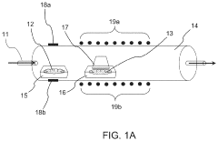
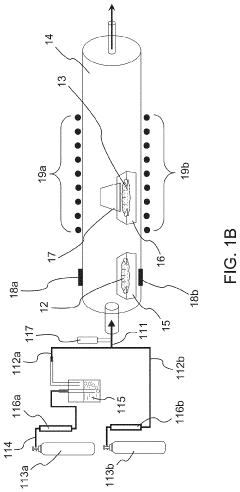
- A method involving chemical vapor deposition (CVD) to form double atomic layer ribbons by depositing monolayers of TMD materials on a substrate, followed by partial removal to create atomic layer nanoribbons, utilizing precursor powders like molybdenum dioxide and sulfur to produce molybdenum disulfide, and subsequent UV-ozone treatment and etching to achieve the desired nanoribbon structure.
Moisture governed growth method of atomic layer ribbons and nanoribbons of transition metal dichalcogenides
PatentActiveUS11639546B2
Innovation
- A method involving chemical vapor deposition (CVD) using precursor powders and a moisturized gas flow to form double and single atomic layer ribbons and nanoribbons, where the process includes depositing monolayers of TMD materials on a substrate, with specific conditions to achieve elongated structures with a length-to-width ratio greater than 500, and subsequent treatments to create nanoribbons.
Materials Science Considerations for TMD Nanoribbon Fabrication
The fabrication of transition metal dichalcogenide (TMD) nanoribbons requires careful consideration of materials science principles to achieve desired edge states. The selection of appropriate TMD materials is paramount, with MoS2, WS2, MoSe2, and WSe2 being the most commonly utilized due to their favorable electronic properties and stability. Each material exhibits distinct band structures and edge state characteristics, necessitating material-specific fabrication approaches.
Crystal structure and orientation significantly impact edge state formation in TMD nanoribbons. The hexagonal lattice structure of TMDs allows for two primary edge terminations: zigzag and armchair. Zigzag edges typically exhibit metallic behavior with magnetic properties, while armchair edges tend to be semiconducting. Controlling the crystallographic orientation during synthesis is therefore critical for engineering specific edge states.
Edge defects and reconstruction phenomena present both challenges and opportunities in nanoribbon fabrication. Dangling bonds at edges create localized states that can be passivated or functionalized to tune electronic properties. Common defects include sulfur vacancies, metal atom dislocations, and edge reconstructions that occur spontaneously to minimize energy. Understanding these defect mechanisms enables intentional defect engineering to achieve desired edge state properties.
Substrate interactions play a crucial role in TMD nanoribbon fabrication and subsequent edge state behavior. Van der Waals forces between the nanoribbon and substrate can induce strain and charge transfer effects that modify edge states. Substrate selection must consider lattice matching, chemical compatibility, and electronic properties. Common substrates include SiO2, hBN, and graphene, each offering different advantages for edge state preservation or modification.
Environmental stability represents a significant challenge in TMD nanoribbon fabrication. Edge states are particularly susceptible to oxidation and other chemical reactions when exposed to ambient conditions. Protective encapsulation using inert materials like hBN or controlled atmosphere processing can preserve edge state integrity. Additionally, the thermal stability of edge states must be considered, as high-temperature processing steps can induce edge reconstruction or defect migration.
Scalable fabrication techniques that maintain precise edge control remain a significant materials science challenge. Top-down approaches like lithography and etching offer precise dimensional control but often introduce edge damage. Bottom-up synthesis methods like chemical vapor deposition can produce cleaner edges but with less precise control over nanoribbon dimensions. Hybrid approaches combining controlled growth with selective etching show promise for achieving both clean edges and dimensional precision.
Quantum Computing Implications of Engineered Edge States
Engineered edge states in TMD nanoribbons present significant implications for quantum computing advancements. These edge states exhibit unique quantum properties that can be harnessed for quantum bit (qubit) implementations with potentially superior coherence times compared to conventional approaches. The topological protection inherent in certain engineered edge states provides natural resistance against environmental decoherence, addressing one of quantum computing's fundamental challenges.
The controlled manipulation of edge states in TMD nanoribbons enables the creation of quantum gates necessary for quantum information processing. By engineering specific edge configurations, researchers can implement quantum logic operations with high fidelity. This approach offers advantages over other quantum computing architectures in terms of scalability and integration potential with existing semiconductor technologies.
Quantum entanglement, a critical resource for quantum computing, can be generated and maintained through properly engineered edge states. The spin-valley coupling characteristics of TMD materials provide additional degrees of freedom for quantum information encoding, potentially enabling more complex quantum algorithms to be executed with fewer physical resources.
For quantum error correction schemes, engineered edge states offer promising platforms. The ability to create arrays of interacting edge states allows for the implementation of surface codes and other topological quantum error correction protocols. This capability significantly enhances the fault tolerance of quantum computing systems based on TMD nanoribbon architectures.
From a practical implementation perspective, TMD-based quantum computing systems could operate at higher temperatures than many competing technologies. While still requiring cooling, the robust nature of engineered edge states may allow operation at temperatures achievable with more conventional refrigeration technologies, reducing infrastructure requirements for quantum computing facilities.
The integration potential with conventional electronics represents another significant advantage. TMD nanoribbons can be fabricated using processes compatible with existing semiconductor manufacturing techniques, potentially accelerating the transition from laboratory demonstrations to practical quantum computing devices. This compatibility may enable hybrid classical-quantum computing architectures that leverage the strengths of both paradigms.
Looking forward, engineered edge states in TMD nanoribbons could contribute to the development of topological quantum computers. These systems would exploit non-Abelian anyons for inherently fault-tolerant quantum computation, potentially circumventing many of the challenges facing current quantum computing approaches and bringing practical, large-scale quantum computers closer to reality.
Unlock deeper insights with Patsnap Eureka Quick Research — get a full tech report to explore trends and direct your research. Try now!
Generate Your Research Report Instantly with AI Agent
Supercharge your innovation with Patsnap Eureka AI Agent Platform!
