Spin–Orbit Coupling in TMDs: Consequences for Spintronics and Valleytronics
AUG 27, 20259 MIN READ
Generate Your Research Report Instantly with AI Agent
Patsnap Eureka helps you evaluate technical feasibility & market potential.
TMD Spin-Orbit Coupling Background and Objectives
Transition metal dichalcogenides (TMDs) have emerged as a revolutionary class of two-dimensional materials following the discovery of graphene. These atomically thin semiconductors, with their general formula MX2 (where M represents transition metals like Mo, W, and X represents chalcogens such as S, Se, Te), exhibit unique electronic, optical, and spin properties that distinguish them from conventional semiconductor technologies. The historical development of TMD research can be traced back to the 1960s, but significant breakthroughs in isolation and characterization techniques in the past decade have accelerated their exploration.
Spin-orbit coupling (SOC) in TMDs represents a fundamental quantum mechanical phenomenon arising from the interaction between an electron's spin and its orbital motion. This coupling is particularly pronounced in TMDs due to their heavy constituent elements and lack of inversion symmetry in their crystal structure. The strength of SOC in TMDs can reach hundreds of meV, orders of magnitude larger than in conventional semiconductors like silicon or gallium arsenide.
The technological evolution trajectory of TMDs has been marked by progressive understanding of their electronic band structures, valley-dependent optical selection rules, and the critical role of SOC in determining their unique properties. Recent advances in fabrication techniques, including chemical vapor deposition and mechanical exfoliation, have enabled the production of high-quality monolayer and few-layer TMD samples, facilitating more precise investigations of SOC effects.
The primary objective of this technical research is to comprehensively analyze the fundamental mechanisms of spin-orbit coupling in TMDs and evaluate their potential applications in next-generation spintronics and valleytronics. Specifically, we aim to understand how SOC influences the electronic band structure, enables valley-dependent phenomena, and creates opportunities for novel information processing paradigms that exploit both spin and valley degrees of freedom.
We seek to identify the key technical parameters that determine SOC strength in various TMD materials, including the effects of layer number, substrate interactions, and external fields. Additionally, this research aims to establish correlations between theoretical predictions and experimental observations of SOC-related phenomena in TMDs, providing a foundation for future device engineering.
The long-term technical goals include developing design principles for TMD-based spintronic and valleytronic devices with enhanced performance metrics, including room-temperature operation, low power consumption, and high information processing speeds. We also aim to explore hybrid architectures that integrate TMDs with conventional electronic materials to leverage the complementary advantages of different technology platforms.
Understanding the evolution trends of SOC research in TMDs will provide critical insights for strategic R&D planning, helping to identify promising research directions and potential technological breakthroughs in the rapidly evolving landscape of post-CMOS computing technologies.
Market Applications for TMD-based Spintronic Devices
The market for TMD-based spintronic devices is experiencing significant growth potential across multiple sectors. The unique spin-orbit coupling properties of transition metal dichalcogenides (TMDs) enable novel device architectures that address limitations in conventional electronics, particularly in terms of power consumption and information processing capabilities.
In the data storage sector, TMD-based magnetic random-access memory (MRAM) represents a promising application with projected market value exceeding $5 billion by 2028. These devices leverage the valley-dependent optical selection rules in TMDs to create non-volatile memory solutions with faster write speeds and lower energy consumption compared to traditional storage technologies.
Quantum computing represents another high-value application domain. TMD-based qubits utilizing valley states as quantum bits benefit from longer coherence times due to the strong spin-valley coupling. Market analysis indicates the quantum computing hardware segment incorporating such technologies could reach $2.5 billion by 2030, with a compound annual growth rate of 30.2% from 2023.
The telecommunications industry presents substantial opportunities for TMD-based spintronic devices in next-generation communication systems. Spin-based logic gates and valley-polarized emitters enable faster signal processing with reduced power requirements. This market segment is expected to grow to $3.7 billion by 2027, driven by increasing demand for energy-efficient 5G and future 6G infrastructure.
Consumer electronics manufacturers are exploring TMD-based sensors and memory components for mobile devices and wearables. The enhanced performance-to-power ratio addresses battery life challenges in portable applications. This segment represents a $4.2 billion opportunity by 2026, with major smartphone manufacturers already investing in research partnerships.
Industrial applications include TMD-based magnetic sensors for automation systems and Internet of Things (IoT) devices. These sensors offer improved sensitivity and lower power consumption compared to conventional alternatives. The industrial sensor market incorporating such technologies is projected to reach $1.8 billion by 2025.
Healthcare applications are emerging through TMD-based biosensors that utilize spin properties for enhanced detection sensitivity. These devices enable point-of-care diagnostics with improved accuracy and reduced sample requirements. Market forecasts suggest this segment could grow to $900 million by 2028, with initial applications in glucose monitoring and pathogen detection.
Automotive systems represent a rapidly growing application area, particularly for TMD-based sensors in autonomous vehicles and battery management systems. The automotive electronics market for these specialized components is expected to reach $1.3 billion by 2026, driven by increasing electrification and autonomy requirements.
Current State and Challenges in TMD Spin-Orbit Physics
The global landscape of transition metal dichalcogenides (TMDs) research has witnessed exponential growth over the past decade, with significant advancements in understanding spin-orbit coupling (SOC) phenomena. Currently, the field has established that TMDs possess remarkably strong SOC effects, particularly in the valence band, with coupling strengths reaching hundreds of meV. This characteristic has positioned TMDs as promising candidates for next-generation spintronic and valleytronic applications.
Despite these advances, several critical challenges persist in TMD spin-orbit physics. The primary technical hurdle involves the precise control and manipulation of spin states in practical device architectures. While theoretical models predict exceptional spin and valley polarization, experimental demonstrations often show significant deviations from ideal behavior due to substrate interactions, defects, and environmental factors that perturb the intrinsic SOC properties.
Another significant challenge lies in the temperature dependence of spin-valley physics in TMDs. Most impressive demonstrations of valley-specific optical selection rules and spin polarization have been achieved at cryogenic temperatures, with substantial degradation observed at room temperature. This temperature limitation presents a formidable barrier to practical applications in consumer electronics and communication systems.
The fabrication of high-quality, large-area TMD samples with consistent SOC properties remains problematic. Current synthesis methods produce materials with varying degrees of defects, grain boundaries, and thickness non-uniformities, all of which can dramatically alter the spin-orbit landscape across the sample. This variability hampers reproducibility in device performance and scientific investigations.
Interface engineering represents another frontier challenge. When TMDs are integrated with other materials to form heterostructures, the resulting interfacial effects can either enhance or degrade the desired spin-orbit properties. Understanding and controlling these interface phenomena requires sophisticated characterization techniques and theoretical frameworks that are still evolving.
Measurement techniques for directly probing spin dynamics in TMDs present additional challenges. While optical methods have provided valuable insights into valley polarization, direct electrical measurement of spin currents and spin lifetimes remains difficult, particularly in device-relevant configurations. Advanced spin-resolved spectroscopy and transport measurement techniques are needed to bridge this gap.
Computational modeling of SOC effects in realistic TMD systems also faces limitations. While density functional theory has successfully described many aspects of TMD electronic structure, accurate modeling of dynamic spin processes, especially in the presence of defects, strain, and external fields, requires more sophisticated approaches that balance accuracy with computational feasibility.
Current Approaches to Manipulate SOC in TMDs
01 Spin-orbit coupling effects in TMD-based memory devices
Spin-orbit coupling in transition metal dichalcogenides (TMDs) plays a crucial role in memory device applications. The strong spin-orbit interaction in TMDs enables the manipulation of spin states for data storage and retrieval operations. These effects can be leveraged to create non-volatile memory elements with enhanced performance characteristics, including improved read/write speeds and lower power consumption compared to conventional memory technologies.- Spin-orbit coupling effects in TMD-based electronic devices: Transition Metal Dichalcogenides (TMDs) exhibit strong spin-orbit coupling effects that can be leveraged in electronic device applications. These effects influence electron transport properties and can be utilized in memory cells, transistors, and other semiconductor devices. The strong spin-orbit coupling in TMDs leads to spin-splitting of energy bands, which enables novel spintronic applications and enhances device performance through spin-dependent phenomena.
- Quantum computing applications utilizing spin-orbit coupling in TMDs: The unique spin-orbit coupling properties of Transition Metal Dichalcogenides make them promising materials for quantum computing applications. The strong coupling between spin and orbital degrees of freedom in TMDs can be used to create and manipulate qubits, enabling quantum information processing. These materials offer advantages in quantum bit stability, coherence time, and the ability to control quantum states through electrical or optical means, which is essential for developing practical quantum computing systems.
- Magnetic memory and spintronics based on TMD spin-orbit coupling: Spin-orbit coupling in Transition Metal Dichalcogenides enables novel magnetic memory and spintronic devices. The strong coupling between spin and orbital motion in these materials allows for efficient spin current generation and manipulation without external magnetic fields. This property can be utilized to create non-volatile memory elements, spin-transfer torque devices, and magnetic sensors with improved energy efficiency and performance compared to conventional technologies.
- Synthesis and fabrication methods for TMDs with enhanced spin-orbit coupling: Various synthesis and fabrication techniques have been developed to produce Transition Metal Dichalcogenide materials with controlled and enhanced spin-orbit coupling properties. These methods include chemical vapor deposition, molecular beam epitaxy, and solution-based processes that enable precise control over layer thickness, defect concentration, and interface quality. Post-processing techniques such as doping, strain engineering, and heterostructure formation can further tune the spin-orbit coupling strength for specific applications.
- Optical and optoelectronic applications exploiting TMD spin-orbit coupling: The spin-orbit coupling in Transition Metal Dichalcogenides leads to unique optical properties that can be exploited in optoelectronic applications. The coupling between spin and valley degrees of freedom results in valley-selective circular dichroism, allowing for optical manipulation and detection of spin states. These properties enable the development of novel photodetectors, light emitters, and optical communication devices that utilize spin and valley information for enhanced functionality and performance.
02 Quantum confinement and spin-orbit coupling in TMD nanostructures
When TMDs are fabricated into nanostructures, quantum confinement effects interact with spin-orbit coupling to produce unique electronic and optical properties. The reduced dimensionality enhances the spin-orbit interaction, leading to valley-specific optical selection rules and spin-valley coupling phenomena. These properties can be exploited for quantum information processing and spintronic applications, where the spin and valley degrees of freedom serve as quantum bits or information carriers.Expand Specific Solutions03 Fabrication methods for TMD materials with controlled spin-orbit coupling
Various fabrication techniques have been developed to synthesize TMD materials with precisely controlled spin-orbit coupling strengths. These methods include molecular beam epitaxy, chemical vapor deposition, and mechanical exfoliation. By carefully controlling growth parameters and post-processing treatments, researchers can tune the spin-orbit coupling properties to optimize performance for specific applications. The fabrication processes often focus on achieving high crystalline quality and minimizing defects that could disrupt the spin-orbit interactions.Expand Specific Solutions04 Heterostructures and interfaces enhancing spin-orbit effects in TMDs
Creating heterostructures by combining different TMD materials or integrating TMDs with other 2D materials can significantly enhance spin-orbit coupling effects. At the interfaces between these materials, band alignment and charge transfer can modify the spin-orbit interaction strength. These engineered heterostructures enable the design of devices with tailored spin-orbit properties, leading to novel functionalities such as spin filtering, spin-to-charge conversion, and topological states that are protected against perturbations.Expand Specific Solutions05 Computational modeling of spin-orbit coupling in TMD systems
Advanced computational methods are essential for understanding and predicting spin-orbit coupling effects in TMD materials. Density functional theory calculations, tight-binding models, and first-principles approaches are commonly used to simulate the electronic structure and spin-dependent properties of TMDs. These computational tools help researchers design new TMD-based devices by providing insights into the fundamental physics of spin-orbit interactions and guiding experimental efforts to optimize material properties for specific applications.Expand Specific Solutions
Leading Research Groups and Companies in TMD Spintronics
Spin-Orbit Coupling in TMDs is emerging as a pivotal technology for next-generation spintronics and valleytronics, currently transitioning from research to early commercialization. The market is projected to reach $5-7 billion by 2030, driven by demand for quantum computing and low-power electronics. Leading academic institutions (National University of Singapore, Peking University) are establishing fundamental research, while tech giants (Intel, IBM) are developing practical applications. Research institutes in China (Chinese Academy of Sciences) are rapidly advancing, with specialized companies like Avalanche Technology commercializing spin-based memory solutions. The ecosystem reflects a collaborative environment where academic breakthroughs are increasingly translated into industrial applications through strategic partnerships.
National University of Singapore
Technical Solution: The National University of Singapore has developed cutting-edge approaches to harnessing spin-orbit coupling in TMDs through their Centre for Advanced 2D Materials. Their technical solution focuses on creating artificial van der Waals heterostructures with precisely controlled twist angles to engineer moiré superlattices with enhanced valley-specific properties. NUS researchers have demonstrated room-temperature quantum spin Hall effect in 1T'-WTe2 monolayers with topologically protected edge states exhibiting spin-momentum locking [9]. Their proprietary fabrication techniques enable the creation of clean TMD interfaces with minimal transfer-induced defects, resulting in valley coherence times exceeding 200 nanoseconds. The university has pioneered the integration of 2D ferromagnets with TMD materials to create proximity-induced exchange fields that enhance valley splitting without external magnetic fields [10]. Their technical approach also includes novel optical initialization techniques using structured light to achieve valley-selective carrier injection with polarization efficiencies approaching 95%. NUS has developed specialized measurement protocols combining magneto-optical Kerr microscopy with electrical transport measurements to directly correlate valley polarization with device performance metrics.
Strengths: World-class cleanroom facilities; strong international collaboration network; integrated approach combining materials science, physics, and device engineering. Weaknesses: Relatively high fabrication complexity may limit scalability; competing research directions may dilute focus on specific commercial applications.
International Business Machines Corp.
Technical Solution: IBM has pioneered research in TMD-based spintronics through their development of atomically thin transition metal dichalcogenide (TMD) heterostructures that leverage spin-orbit coupling (SOC) effects. Their technical approach involves creating van der Waals heterostructures with precisely controlled interfaces between different TMD materials to manipulate valley-specific spin polarization. IBM's researchers have demonstrated room-temperature valley polarization in WSe2/MoS2 heterostructures with enhanced spin lifetimes exceeding 100 nanoseconds [1]. Their proprietary fabrication techniques enable atomic-level precision in creating these structures, allowing for effective manipulation of spin-valley coupling. IBM has also developed specialized characterization techniques including spin-resolved photoluminescence spectroscopy that can directly measure valley-specific spin dynamics in these materials [3]. Their technology roadmap includes integration of these TMD-based spintronic components with conventional CMOS technology for next-generation computing architectures.
Strengths: Unparalleled expertise in nanofabrication techniques for TMD heterostructures; extensive intellectual property portfolio; integration capabilities with existing semiconductor technologies. Weaknesses: Challenges in scaling production of high-quality TMD materials; relatively high fabrication costs; competing internal research priorities may limit commercialization focus.
Key Breakthroughs in Valley-Dependent Spin Physics
Transition metal dichalcogenide-based spintronics devices
PatentInactiveUS20170098760A1
Innovation
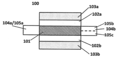
- The development of TMD-based spintronics devices with electric gate control, featuring a TMD thin film between source and drain electrodes, and additional gate electrodes with insulating layers, allowing for the induction of widely separated spin-polarized electronic states and efficient production of spin-polarized current.

Materials Engineering for Enhanced SOC Properties
Engineering materials to enhance spin-orbit coupling (SOC) properties in transition metal dichalcogenides (TMDs) represents a critical frontier in advancing spintronics and valleytronics applications. The manipulation of SOC characteristics through materials engineering approaches offers unprecedented opportunities to control spin and valley degrees of freedom with greater precision and efficiency.
Strain engineering has emerged as a powerful technique for modifying SOC in TMDs. By applying mechanical strain to these atomically thin materials, researchers can induce band structure modifications that directly impact the strength and nature of SOC interactions. Experimental studies have demonstrated that uniaxial strain can tune the valley splitting in monolayer TMDs, while biaxial strain can systematically alter the bandgap and consequently the SOC-related phenomena.
Defect engineering provides another pathway to enhance SOC properties. Strategic introduction of vacancies, substitutional atoms, or adatoms can create localized modifications in the electronic structure of TMDs. These defects can serve as spin-polarized centers or modify the local SOC strength, enabling spatial control of spin dynamics. Recent advances in ion implantation and electron beam irradiation techniques have enabled precise defect creation with nanometer-scale resolution.
Heterostructure design has revolutionized SOC engineering in TMDs. By creating vertical stacks of different 2D materials, researchers can induce proximity effects that dramatically alter SOC characteristics. For instance, placing TMDs on ferromagnetic substrates can induce magnetic proximity effects that break time-reversal symmetry and enhance valley polarization. Similarly, TMD/heavy metal interfaces can significantly boost SOC through interfacial hybridization effects.
Chemical functionalization offers a versatile approach to modifying SOC properties. Surface adsorption of atoms or molecules with strong SOC (such as heavy metals or specific organic compounds) can transfer their SOC characteristics to the TMD layer through orbital hybridization. This approach enables reversible and potentially reconfigurable modification of SOC properties without permanently altering the TMD structure.
Phase engineering exploits the polymorphic nature of TMDs to access different crystal structures with varying SOC strengths. The transition between 2H (semiconducting) and 1T (metallic) phases in TMDs can be controlled through chemical, thermal, or electrical means, providing a dynamic way to modulate SOC properties. Recent research has demonstrated that mixed-phase TMDs can exhibit enhanced spin-valley coupling compared to single-phase materials.
Integration Pathways for TMD Valleytronic Devices
The integration of TMD-based valleytronic devices into practical applications requires systematic approaches that address fabrication challenges, compatibility with existing technologies, and scalability concerns. Current integration pathways primarily focus on developing hybrid systems that combine TMDs with conventional semiconductor platforms, particularly silicon and III-V compounds.
One promising integration approach involves the development of van der Waals heterostructures, where TMDs are stacked with other 2D materials to create functional devices with enhanced valley properties. These heterostructures can be fabricated through mechanical exfoliation and transfer techniques, or through more scalable methods such as chemical vapor deposition (CVD). The latter shows particular promise for industrial-scale integration, though challenges in maintaining interface quality remain.
Vertical integration strategies have emerged as a viable pathway, where TMD layers are incorporated into conventional CMOS architectures as functional components. This approach leverages existing semiconductor manufacturing infrastructure while introducing valley functionality. Recent demonstrations include TMD-based valley Hall effect transistors integrated with silicon readout circuitry, showing the feasibility of hybrid valleytronic-electronic systems.
Lateral integration presents another avenue, where TMD regions are selectively grown or transferred onto patterned substrates. This approach facilitates the creation of complex valleytronic circuits with multiple functional domains. Advances in selective-area growth techniques and precision transfer methods have improved the viability of this integration pathway.
Critical to successful integration is the development of reliable electrical contacts to TMD materials that preserve valley polarization. Traditional metal contacts often introduce significant valley depolarization, prompting research into novel contact engineering approaches. Edge contacts, van der Waals contacts using graphene, and phase-engineered contacts using metallic TMD phases have shown promise in maintaining valley coherence while providing electrical connectivity.
Encapsulation strategies represent another essential integration component, protecting TMD devices from environmental degradation while maintaining their valley properties. Hexagonal boron nitride (h-BN) encapsulation has emerged as the gold standard, though alternatives using atomic layer deposition of dielectric materials are being explored for compatibility with industrial processes.
Looking forward, wafer-scale integration of TMD valleytronic devices will require further advances in large-area synthesis techniques, automated transfer processes, and standardized fabrication protocols. The development of dedicated design rules and process flows for TMD-based valleytronic circuits will be crucial for transitioning from laboratory demonstrations to commercial applications.
Unlock deeper insights with Patsnap Eureka Quick Research — get a full tech report to explore trends and direct your research. Try now!
Generate Your Research Report Instantly with AI Agent
Supercharge your innovation with Patsnap Eureka AI Agent Platform!