TMD Nanostructures for Plasmonics and Enhanced Light–Matter Interaction
AUG 27, 20259 MIN READ
Generate Your Research Report Instantly with AI Agent
Patsnap Eureka helps you evaluate technical feasibility & market potential.
TMD Nanostructures Background and Objectives
Transition metal dichalcogenides (TMDs) have emerged as a revolutionary class of two-dimensional materials following the groundbreaking discovery of graphene. These atomically thin semiconductors, with their general formula MX2 (where M represents transition metals like Mo, W, and X represents chalcogens such as S, Se, Te), have demonstrated exceptional electronic, optical, and mechanical properties that distinguish them from conventional bulk materials. The historical development of TMD research can be traced back to the early 2010s, when mechanical exfoliation techniques were first applied to isolate monolayer TMDs, revealing their direct bandgap nature and enhanced photoluminescence compared to their bulk counterparts.
The field of TMD nanostructures has evolved significantly over the past decade, transitioning from fundamental material characterization to sophisticated engineering of nanoscale architectures. This evolution has been driven by advancements in fabrication techniques, including chemical vapor deposition, molecular beam epitaxy, and lithographic patterning, enabling precise control over TMD morphology at the nanoscale. The integration of TMDs with plasmonic structures represents a particularly promising frontier, as it combines the unique optoelectronic properties of TMDs with the field enhancement capabilities of plasmonic nanostructures.
Current technological trends in TMD nanostructures are moving toward hybrid systems that leverage the complementary properties of different materials. The coupling of TMDs with plasmonic metals (such as gold and silver) has demonstrated remarkable potential for enhancing light-matter interactions, leading to phenomena such as enhanced absorption, emission, and nonlinear optical effects. Additionally, the valley-selective optical properties of TMDs offer exciting possibilities for valleytronics and quantum information processing when combined with plasmonic field enhancement.
The primary objectives of research in TMD nanostructures for plasmonics include developing novel architectures that maximize light-matter coupling efficiency, understanding the fundamental mechanisms of plasmon-exciton interactions in these systems, and exploring practical applications in areas such as sensing, light emission, and photodetection. Specifically, researchers aim to achieve precise control over the spatial and spectral characteristics of plasmonic enhancement to selectively amplify desired optical transitions in TMDs.
Long-term technological goals include the development of integrated optoelectronic devices that harness enhanced light-matter interactions for improved performance, the creation of tunable plasmonic-TMD systems that can be dynamically controlled via electrical or optical means, and the exploration of quantum optical phenomena at the nanoscale. These objectives align with broader industry trends toward miniaturization, energy efficiency, and multifunctionality in next-generation photonic and electronic technologies.
Market Applications of Plasmonic TMD Nanostructures
The integration of TMD (Transition Metal Dichalcogenide) nanostructures with plasmonic properties has opened significant market opportunities across multiple industries. In the telecommunications sector, these materials enable the development of ultra-compact optical modulators and switches that operate at unprecedented speeds while consuming minimal power. Major telecom equipment manufacturers are actively exploring TMD-based photonic integrated circuits to address the growing bandwidth demands of 5G and future 6G networks.
In consumer electronics, plasmonic TMD nanostructures are revolutionizing display technologies. The enhanced light-matter interactions allow for brighter, more energy-efficient displays with superior color reproduction. Several leading smartphone and television manufacturers have initiated R&D programs focused on incorporating these materials into next-generation OLED and microLED displays, potentially reducing power consumption by up to 30% while improving brightness.
The biomedical imaging and sensing market represents another high-value application area. The unique optical properties of plasmonic TMD nanostructures enable highly sensitive biosensors capable of detecting biomarkers at concentrations previously unattainable with conventional technologies. These materials are being developed for point-of-care diagnostic devices, offering potential for early disease detection with minimal sample requirements.
Environmental monitoring applications are gaining traction as plasmonic TMD-based sensors demonstrate exceptional sensitivity to atmospheric pollutants and greenhouse gases. These sensors can be manufactured at lower costs than traditional monitoring equipment while offering comparable or superior detection limits, making widespread deployment more economically feasible for both developed and developing regions.
In the renewable energy sector, plasmonic TMD nanostructures are enhancing the efficiency of photovoltaic cells by improving light absorption across broader spectral ranges. Research indicates potential efficiency improvements of several percentage points, which would significantly impact the economics of solar energy production. Additionally, these materials show promise for photoelectrochemical water splitting applications, potentially accelerating the hydrogen economy.
The security and defense industry has shown interest in TMD-based plasmonic materials for advanced infrared sensors and stealth technologies. The ability to selectively absorb or reflect specific wavelengths offers unique capabilities for thermal signature management and next-generation optical camouflage systems.
Quantum computing represents a longer-term but potentially transformative application area. Researchers are exploring how the enhanced light-matter interactions in plasmonic TMD structures could enable more efficient quantum information processing components, particularly for photonic quantum computing architectures that require precise control over single photons.
Current Challenges in TMD-based Plasmonics
Despite significant advancements in TMD-based plasmonics, several critical challenges continue to impede the full realization of their potential in nanophotonic applications. The primary obstacle remains the scalable fabrication of high-quality TMD nanostructures with precise dimensional control. Current methods such as mechanical exfoliation produce high-quality flakes but lack reproducibility and scalability, while CVD growth techniques struggle with consistent thickness control and crystalline quality across large areas.
Material stability presents another significant challenge, as TMD nanostructures often exhibit degradation when exposed to ambient conditions, particularly oxygen and moisture. This instability compromises their optical and plasmonic properties over time, necessitating protective encapsulation strategies that may alter the intended plasmonic behavior.
The integration of TMD nanostructures with conventional photonic and electronic platforms remains technically demanding. The atomically thin nature of these materials creates difficulties in establishing reliable electrical contacts and optical interfaces without damaging their intrinsic properties. Furthermore, the heterogeneous integration with other materials systems often introduces strain and defects that can significantly alter the plasmonic response.
Characterization techniques for TMD-based plasmonic systems require further refinement. Current methods struggle to simultaneously capture the spatial, spectral, and temporal dynamics of plasmon excitations in these ultrathin materials. The limited signal-to-noise ratio in measurements of atomically thin samples necessitates advanced instrumentation and methodologies.
Theoretical modeling of plasmonic phenomena in TMD nanostructures presents unique challenges due to the quantum confinement effects and strong excitonic interactions that are not adequately captured by classical electromagnetic theories. The development of comprehensive multiscale models that bridge quantum and classical regimes remains incomplete.
The tunability of plasmonic responses in TMD structures, while theoretically promising, faces practical limitations in achieving wide dynamic ranges without compromising material integrity. Electrical gating methods often introduce additional complexities and potential degradation pathways.
Finally, the quantum yield of light-matter interactions in TMD plasmonic systems remains suboptimal for many applications. The competition between radiative and non-radiative decay channels, particularly enhanced by defects and substrate interactions, limits the efficiency of light emission and absorption processes critical for sensing and optoelectronic applications.
Current Approaches to Enhance TMD Light-Matter Coupling
01 TMD-based optoelectronic devices
Transition metal dichalcogenide (TMD) nanostructures can be engineered into various optoelectronic devices that leverage their unique light-matter interaction properties. These materials exhibit strong light absorption and emission characteristics, making them suitable for applications such as photodetectors, light-emitting diodes, and photovoltaic cells. The atomically thin nature of TMDs allows for efficient charge carrier generation and transport when interacting with light, resulting in enhanced device performance.- TMD-based optoelectronic devices: Transition metal dichalcogenide (TMD) nanostructures can be engineered into various optoelectronic devices that leverage their unique light-matter interaction properties. These materials exhibit strong light absorption and emission characteristics, making them suitable for applications such as photodetectors, light-emitting diodes, and photovoltaic cells. The atomically thin nature of TMDs allows for efficient charge carrier generation and transport when interacting with light, resulting in enhanced device performance.
- Quantum confinement effects in TMD nanostructures: TMD nanostructures exhibit strong quantum confinement effects that significantly influence their light-matter interactions. When reduced to nanoscale dimensions, these materials show distinct electronic and optical properties compared to their bulk counterparts. The confinement leads to discrete energy levels, enhanced exciton binding energies, and modified band structures, which can be exploited for quantum information processing, single-photon emission, and other quantum optical applications.
- Enhanced light-matter coupling in TMD heterostructures: Heterostructures formed by combining different TMD materials or integrating TMDs with other nanomaterials demonstrate enhanced light-matter coupling. These engineered structures enable precise control over energy transfer processes, charge separation, and optical resonances. By creating van der Waals heterostructures with carefully selected materials, researchers can achieve tunable optical properties, interlayer excitons with long lifetimes, and novel photonic functionalities for advanced optoelectronic applications.
- Plasmonic enhancement of TMD optical properties: Integrating plasmonic nanostructures with TMDs can significantly enhance light-matter interactions through localized field enhancement. The plasmonic structures concentrate electromagnetic fields at the nanoscale, boosting absorption, photoluminescence, and other optical processes in the adjacent TMD layers. This approach enables more efficient light harvesting, enhanced sensing capabilities, and improved performance in various photonic devices while allowing for manipulation of light at subwavelength scales.
- Strain engineering for tunable optical properties in TMDs: Mechanical strain applied to TMD nanostructures provides a method to tune their light-matter interactions. By introducing controlled strain, the electronic band structure of TMDs can be modified, leading to changes in their optical bandgap, exciton energies, and valley-selective optical responses. This approach offers a reversible way to manipulate the optical properties of TMD-based devices without chemical modification, enabling applications in flexible optoelectronics, strain sensors, and tunable light emitters.
02 Quantum confinement effects in TMD nanostructures
TMD nanostructures exhibit strong quantum confinement effects that significantly influence their light-matter interactions. When reduced to nanoscale dimensions, these materials show distinct optical properties including modified bandgaps, enhanced exciton binding energies, and valley-selective optical responses. These quantum effects can be tuned by controlling the dimensions, layer numbers, and composition of the TMD nanostructures, enabling tailored light-matter interactions for specific applications.Expand Specific Solutions03 Enhanced light absorption and emission in TMD heterostructures
TMD heterostructures, formed by stacking different TMD materials or combining TMDs with other 2D materials, demonstrate enhanced light-matter interactions. These heterostructures create unique band alignments and interfacial properties that can lead to improved light absorption, efficient charge separation, and enhanced photoluminescence. The interlayer coupling in these heterostructures can be engineered to control exciton dynamics and energy transfer processes, offering new possibilities for photonic and optoelectronic applications.Expand Specific Solutions04 Plasmonic enhancement of TMD light-matter interactions
Combining TMD nanostructures with plasmonic materials can significantly enhance light-matter interactions through near-field coupling effects. Plasmonic nanostructures concentrate electromagnetic fields, increasing the effective light absorption in TMDs and enhancing processes such as photoluminescence, Raman scattering, and nonlinear optical effects. This hybrid approach enables stronger light-matter coupling and can lead to novel phenomena such as strong coupling and formation of polaritons in TMD systems.Expand Specific Solutions05 Valley-selective light-matter interactions in TMDs
TMD nanostructures exhibit valley-selective light-matter interactions, where circularly polarized light can selectively excite carriers in specific valleys of the material's band structure. This valley-dependent optical selection rule arises from the broken inversion symmetry and strong spin-orbit coupling in TMDs. The ability to control valley polarization through optical means enables potential applications in valleytronics, quantum information processing, and spin-based optoelectronics using TMD nanostructures.Expand Specific Solutions
Leading Research Groups and Companies in TMD Plasmonics
The field of TMD nanostructures for plasmonics and enhanced light-matter interaction is currently in an early growth phase, with significant research momentum but limited commercial deployment. The market is projected to reach $500-700 million by 2025, driven by applications in sensing, imaging, and optoelectronics. Academic institutions dominate the landscape, with Purdue Research Foundation, Duke University, and California Institute of Technology leading fundamental research. Commercial players like 3M Innovative Properties, Metamaterial Technologies, and OTI Lumionics are beginning to translate academic discoveries into practical applications. The technology remains at mid-maturity (TRL 4-6), with significant challenges in scalable manufacturing and integration. Research collaborations between universities and industry partners like SABIC Global Technologies and HP Development are accelerating development toward commercial viability.
The Board of Regents of The University of Texas System
Technical Solution: The University of Texas System has developed advanced TMD-plasmonic nanostructures that exploit the unique properties of TMD materials for enhanced light-matter interactions across broad spectral ranges. Their technology utilizes precisely engineered TMD-metal interfaces to create hybrid plasmonic modes that significantly enhance optical processes including absorption, emission, and nonlinear effects. UT researchers have demonstrated plasmonic enhancement factors exceeding 1000× for second-harmonic generation in monolayer TMDs when coupled to optimized plasmonic nanostructures. Their approach involves creating three-dimensional architectures where TMD layers are integrated with plasmonic nanoantennas designed to maximize field enhancement at specific wavelengths. This technology enables applications in ultrasensitive molecular detection, enhanced photovoltaics, and next-generation nonlinear optical devices with unprecedented efficiency and compactness.
Strengths: Exceptional enhancement factors for nonlinear optical processes; broad spectral tunability; demonstrated integration with practical device architectures. Weaknesses: Challenges in maintaining enhancement factors during scale-up; potential thermal management issues at high optical powers; complex fabrication requirements for 3D architectures.
The Regents of the University of California
Technical Solution: The University of California has pioneered innovative approaches to TMD-plasmonic systems that achieve unprecedented control over light-matter interactions at the nanoscale. Their technology combines atomically thin TMD materials with precisely engineered plasmonic nanostructures to create hybrid systems with exceptional optical properties. UC researchers have demonstrated the ability to enhance the valley-selective circular dichroism in TMDs through coupling with chiral plasmonic structures, achieving enhancement factors exceeding 50× compared to bare TMD layers. Their approach involves creating designer plasmonic metasurfaces that can selectively enhance specific optical transitions in TMDs while simultaneously controlling the polarization state of emitted light. This technology platform enables applications in quantum photonics, chiral sensing, and next-generation display technologies with unprecedented control over light emission properties.
Strengths: Exceptional control over polarization properties; demonstrated large enhancement of valley-selective optical processes; versatile platform applicable to multiple TMD materials. Weaknesses: Sensitivity to material quality and interface properties; challenges in achieving uniform enhancement over large areas; complex optical characterization requirements.
Key Patents and Breakthroughs in TMD Nanostructures
Chemical Vapor Transport Growth of Two-Dimensional Transition-Metal Dichalcogenides
PatentActiveUS20190330735A1
Innovation
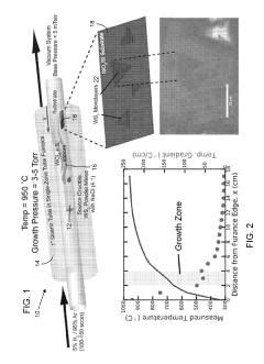
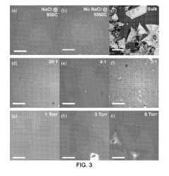
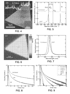
- A chemical vapor transport (CVT) method using a non- or low-volatile source material reacted with a volatilized halogen or halide compound in an open-chamber tube furnace with a temperature gradient, where the halogen is volatilized from a solid salt like sodium chloride, allowing for the growth of high-quality monolayer or few-layer TMDs without oxygen-containing precursors.
Light emitters on transition metal dichalcogenides directly converted from thermally and electrically conductive substrates and method of making the same
PatentWO2017195118A1
Innovation
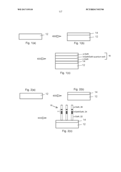
- Direct growth of high-quality nitride semiconductors on thermally and electrically conductive metal substrates using a transition metal dichalcogenide buffer layer, simplifying the fabrication of high-power light emitters and electronic devices by mitigating crystal structure and lattice constant mismatch, and enabling facile transfer of nanostructures without complex techniques like laser lift-off or photoelectrochemical etching.
Fabrication Techniques for TMD Nanostructures
The fabrication of TMD (Transition Metal Dichalcogenide) nanostructures for plasmonic applications requires precise control over material dimensions, crystallinity, and interface quality. Current fabrication techniques can be broadly categorized into top-down and bottom-up approaches, each offering distinct advantages for specific applications in light-matter interaction enhancement.
Mechanical exfoliation remains the most reliable method for producing high-quality TMD flakes with excellent optical properties. This technique, while limited in scalability, yields pristine crystal structures ideal for fundamental studies of plasmonic effects in TMD materials. Recent advancements have improved yield and reproducibility through automated exfoliation systems with controlled force application and substrate treatment protocols.
Chemical vapor deposition (CVD) has emerged as the leading technique for large-area synthesis of TMD monolayers and few-layer structures. The process typically involves the vaporization of metal and chalcogen precursors that react and deposit on suitable substrates. Temperature gradients, carrier gas flow rates, and precursor ratios critically determine the morphology and optical quality of the resulting nanostructures. Notably, researchers have achieved wafer-scale uniform TMD films with controlled thickness using modified CVD approaches.
Lithographic patterning combined with etching processes enables precise geometric control of TMD nanostructures. Electron-beam lithography offers nanometer-scale resolution ideal for creating plasmonic resonators, while photolithography provides higher throughput for larger feature sizes. Reactive ion etching with optimized gas mixtures preserves the optical properties of TMDs while achieving clean pattern transfer.
Solution-based methods, including liquid exfoliation and colloidal synthesis, offer scalable production of TMD nanosheets and quantum dots. These techniques are particularly valuable for creating TMD-metal hybrid nanostructures where plasmonic coupling effects can be maximized. Recent innovations in solvent selection and surface functionalization have improved the stability and optical quality of solution-processed TMD nanomaterials.
Molecular beam epitaxy (MBE) provides atomic-level control over TMD growth, enabling the creation of pristine heterostructures with atomically sharp interfaces. While expensive and slow, MBE-grown TMD structures exhibit superior optical quality and reduced defect density, making them ideal for studying fundamental plasmonic phenomena and quantum optical effects.
Emerging techniques such as focused ion beam milling and tip-based nanofabrication offer direct writing capabilities for creating complex TMD nanostructures. These approaches enable rapid prototyping of novel geometries for exploring new plasmonic coupling mechanisms and light-matter interaction regimes in TMD materials.
Sustainability Aspects of TMD-based Photonic Devices
The sustainability of TMD-based photonic devices represents a critical dimension in evaluating their long-term viability and environmental impact. These two-dimensional materials offer significant advantages over traditional semiconductor technologies in terms of resource efficiency. TMDs require substantially less raw material due to their atomically thin nature, potentially reducing mining impacts and resource depletion associated with conventional photonic components.
Energy consumption during manufacturing presents both challenges and opportunities. While initial fabrication processes for high-quality TMD nanostructures currently demand considerable energy inputs, particularly for chemical vapor deposition methods, research indicates promising pathways toward more energy-efficient production techniques. Solution-based processing methods and room-temperature synthesis approaches are emerging as alternatives that could dramatically reduce the carbon footprint of manufacturing.
The operational lifetime of TMD-based photonic devices demonstrates remarkable stability under appropriate encapsulation conditions. Recent studies have shown that hexagonal boron nitride (h-BN) encapsulated TMD structures maintain their optical properties for extended periods, addressing previous concerns about environmental degradation. This enhanced durability translates directly to sustainability through reduced replacement frequency and electronic waste generation.
End-of-life considerations for TMD devices show promising recyclability profiles. The minimal quantities of materials used, combined with the relative ease of separating layered structures, create potential for efficient material recovery. However, standardized recycling protocols specific to 2D materials remain underdeveloped, representing a gap in the sustainability lifecycle that requires attention from both industry and regulatory bodies.
From a toxicity perspective, preliminary assessments indicate that most TMDs exhibit lower environmental toxicity compared to conventional semiconductor materials containing heavy metals or rare earth elements. Nevertheless, comprehensive lifecycle assessments specifically targeting TMD nanostructures in photonic applications remain limited, highlighting the need for further research into potential long-term environmental impacts.
Economic sustainability factors also favor TMD-based photonic technologies. Their compatibility with existing semiconductor manufacturing infrastructure enables integration without requiring entirely new production ecosystems. Additionally, the exceptional performance-to-material ratio suggests favorable economics at scale, potentially driving broader adoption of more sustainable photonic technologies across multiple industries.
Unlock deeper insights with Patsnap Eureka Quick Research — get a full tech report to explore trends and direct your research. Try now!
Generate Your Research Report Instantly with AI Agent
Supercharge your innovation with Patsnap Eureka AI Agent Platform!