TMDs in Flexible Electronics: Mechanical Robustness and Device Integration
AUG 27, 20259 MIN READ
Generate Your Research Report Instantly with AI Agent
PatSnap Eureka helps you evaluate technical feasibility & market potential.
TMDs Evolution and Integration Goals
Transition metal dichalcogenides (TMDs) have emerged as a revolutionary class of two-dimensional materials following the discovery of graphene. The evolution of TMDs research has progressed from fundamental material characterization to advanced applications in flexible electronics over the past decade. Initially, researchers focused on understanding the unique electronic properties of TMDs, such as their direct bandgap in monolayer form and strong spin-orbit coupling, which differentiated them from graphene's zero-bandgap limitation.
The technological trajectory of TMDs has been marked by significant milestones, including the first demonstration of monolayer MoS2 transistors in 2011, which exhibited mobility values exceeding 200 cm²/Vs and on/off ratios of 10⁸. This breakthrough catalyzed extensive research into various TMD materials including WS2, MoSe2, and WSe2, each offering distinct electronic and optical properties suitable for different applications in flexible electronics.
Recent advancements have shifted toward addressing the mechanical robustness challenges that are critical for flexible device integration. The inherent atomic thinness of TMDs provides natural flexibility, but integration with substrate materials and encapsulation layers presents complex interfaces that must withstand repeated bending, stretching, and twisting without performance degradation.
The primary technical goals for TMDs in flexible electronics center on achieving reliable mechanical performance while maintaining electronic functionality. This includes developing transfer techniques that preserve material integrity, creating robust contacts that maintain conductivity under deformation, and designing device architectures that distribute strain effectively. Current research aims to achieve devices that can withstand bending radii below 1 mm and more than 10,000 bending cycles without significant performance loss.
Integration goals extend beyond mechanical considerations to include scalable manufacturing processes compatible with existing electronics fabrication infrastructure. Chemical vapor deposition (CVD) has emerged as a promising approach for large-area synthesis, though challenges in controlling layer uniformity and defect density remain. Solution-processed TMDs offer an alternative pathway, with recent advances in liquid exfoliation techniques showing promise for industrial-scale production.
The technological evolution is now trending toward heterogeneous integration, where TMDs are combined with other 2D materials and conventional semiconductors to create hybrid systems with enhanced functionality. These van der Waals heterostructures represent the next frontier, enabling novel device concepts such as atomically thin p-n junctions, tunneling transistors, and photodetectors with tailored spectral responses.
Looking forward, the field is progressing toward self-healing interfaces and intrinsically stretchable TMD-based devices that can accommodate not just bending but also tensile strain exceeding 50%. These developments align with the broader goal of creating truly conformable electronics that can seamlessly integrate with irregular surfaces, including biological tissues for advanced bioelectronic applications.
Market Analysis for Flexible Electronics
The flexible electronics market has witnessed remarkable growth in recent years, with a global market value reaching $41.2 billion in 2022 and projected to grow at a CAGR of 15.3% through 2030. This expansion is driven by increasing demand for portable, lightweight, and conformable electronic devices across various sectors including consumer electronics, healthcare, automotive, and aerospace.
Transition metal dichalcogenides (TMDs) have emerged as critical materials in this market due to their exceptional mechanical properties and electrical characteristics. The integration of TMDs in flexible electronics addresses key market requirements for devices that can withstand bending, folding, and stretching while maintaining performance integrity.
Consumer electronics represents the largest application segment, accounting for approximately 38% of the flexible electronics market. Within this segment, foldable displays incorporating TMDs have gained significant traction, with major manufacturers like Samsung, LG, and Huawei investing heavily in this technology. The foldable smartphone market alone grew by 264% in 2021, indicating strong consumer acceptance and market potential for TMD-based flexible devices.
Healthcare applications present another substantial growth opportunity, particularly in wearable health monitoring devices and implantable electronics. The medical wearables market is expected to reach $19.5 billion by 2025, with TMD-based flexible sensors playing an increasingly important role due to their biocompatibility and mechanical robustness.
Regional analysis reveals Asia-Pacific as the dominant market for flexible electronics, holding 45% of the global market share. This is attributed to the strong presence of electronics manufacturing facilities and increasing R&D investments in countries like South Korea, Japan, and China. North America follows with 28% market share, driven by technological innovation and early adoption of advanced electronic solutions.
Key market challenges include high production costs and scalability issues. The average manufacturing cost for TMD-based flexible electronics remains 30-40% higher than conventional rigid electronics, presenting a significant barrier to mass market adoption. However, recent advancements in production techniques have begun to narrow this gap.
Market forecasts indicate that TMD-based flexible electronics will experience accelerated growth as manufacturing processes mature and economies of scale are achieved. The specific segment of TMD-integrated flexible devices is projected to grow at 22% annually through 2028, outpacing the broader flexible electronics market.
Investor confidence in this technology is evidenced by venture capital funding exceeding $2.3 billion in 2022 for startups focused on advanced materials for flexible electronics, with TMD-related ventures securing approximately 18% of this funding.
Current Challenges in TMDs Mechanical Robustness
Despite the promising properties of transition metal dichalcogenides (TMDs) for flexible electronics, significant challenges persist regarding their mechanical robustness. The atomically thin nature of TMDs makes them inherently susceptible to mechanical damage during fabrication, integration, and operation. When subjected to bending, folding, or stretching, TMDs often develop microcracks that propagate rapidly across the material, leading to catastrophic device failure.
The interface adhesion between TMDs and flexible substrates presents another critical challenge. Poor adhesion results in delamination under mechanical stress, compromising device performance and reliability. Current transfer methods, including wet and dry transfer techniques, frequently introduce defects and contamination that further weaken mechanical integrity.
Strain engineering in TMDs remains problematic as these materials exhibit anisotropic mechanical properties, with different elastic responses along various crystallographic directions. This anisotropy complicates the prediction and control of mechanical behavior in flexible device architectures. Furthermore, the strain distribution in TMDs is often non-uniform, creating localized stress concentrations that become failure initiation points.
The grain boundaries in polycrystalline TMD films represent significant mechanical weak points. These boundaries exhibit lower fracture toughness compared to the pristine crystal domains, making them particularly vulnerable to crack formation and propagation under mechanical deformation. The challenge is exacerbated in large-area TMD films, which typically contain numerous grain boundaries.
Environmental factors also severely impact the mechanical stability of TMDs. Exposure to moisture, oxygen, and other atmospheric components accelerates degradation of mechanical properties through chemical reactions at defect sites and edges. This environmental sensitivity necessitates effective encapsulation strategies, which themselves must maintain flexibility without compromising the mechanical properties of the underlying TMD layer.
Characterization of mechanical properties presents methodological challenges. Conventional techniques for measuring mechanical parameters such as Young's modulus, fracture toughness, and fatigue resistance are difficult to apply to atomically thin materials. This limitation hinders quantitative understanding and systematic improvement of TMD mechanical robustness.
The scalability of fabrication processes that maintain mechanical integrity remains elusive. While laboratory-scale demonstrations have shown promising results, translating these to industrial-scale production while preserving mechanical robustness has proven challenging. Current growth and transfer methods that yield mechanically robust TMDs are often incompatible with large-scale manufacturing requirements.
Current Integration Solutions for TMDs
01 Mechanical reinforcement of TMDs through composite structures
Transition Metal Dichalcogenides (TMDs) can be mechanically reinforced by incorporating them into composite structures. These composites typically combine TMDs with other materials such as polymers, carbon-based materials, or ceramics to enhance their mechanical robustness. The resulting composites demonstrate improved tensile strength, flexibility, and resistance to mechanical deformation while maintaining the desirable electronic and optical properties of TMDs.- Structural reinforcement techniques for TMD materials: Various structural reinforcement techniques can be applied to enhance the mechanical robustness of Transition Metal Dichalcogenides (TMDs). These include creating composite structures, incorporating supporting substrates, and developing specialized layering techniques that distribute mechanical stress. These methods help prevent fracturing and delamination under physical strain, significantly improving the durability and flexibility of TMD-based devices while maintaining their unique electronic and optical properties.
- Fabrication methods to improve mechanical stability: Advanced fabrication methods can significantly enhance the mechanical robustness of TMD materials. Techniques such as controlled vapor deposition, epitaxial growth, and specialized annealing processes create more defect-free and structurally sound TMD layers. These methods focus on optimizing crystal growth conditions to minimize structural weaknesses and grain boundaries that typically serve as failure points under mechanical stress, resulting in TMD materials with superior mechanical properties.
- Encapsulation and protection strategies: Encapsulation and protection strategies play a crucial role in enhancing the mechanical robustness of TMD materials. By applying protective layers or encapsulating TMDs within flexible polymers or between inert materials, these approaches shield the sensitive TMD structures from environmental factors and mechanical damage. These protection methods effectively preserve the structural integrity and functional properties of TMDs even under bending, stretching, or other mechanical deformations.
- Strain engineering and flexibility enhancement: Strain engineering techniques can be employed to enhance the flexibility and mechanical robustness of TMD materials. By deliberately introducing controlled strain patterns or designing structures that can accommodate deformation, these approaches allow TMD-based devices to withstand bending, folding, and stretching without performance degradation. This engineering approach transforms inherently brittle TMD materials into components suitable for flexible and wearable electronics applications.
- Interface and defect management for improved durability: Managing interfaces and defects is critical for improving the mechanical durability of TMD materials. Techniques such as interface engineering, defect passivation, and controlled doping can strengthen the weak points in TMD structures. By addressing these vulnerabilities, the overall mechanical robustness of TMD-based devices is enhanced, allowing them to withstand mechanical stresses and strains while maintaining their electrical and optical functionality over extended periods of operation.
02 Substrate engineering for enhanced TMD mechanical stability
The mechanical robustness of TMDs can be significantly improved through careful substrate engineering. By selecting appropriate substrate materials and optimizing the interface between the TMD and substrate, strain can be managed and mechanical stability enhanced. Various techniques including epitaxial growth on lattice-matched substrates, flexible substrate integration, and buffer layer insertion can be employed to minimize lattice mismatch and improve adhesion, resulting in TMD structures with superior mechanical properties.Expand Specific Solutions03 Defect engineering and doping strategies for TMDs
Controlled introduction of defects and dopants into TMD structures can enhance their mechanical robustness. By carefully engineering vacancies, substitutional atoms, or grain boundaries, the mechanical properties of TMDs can be tuned. Doping with specific elements can strengthen interlayer bonding and improve resistance to mechanical deformation. These approaches allow for the development of TMDs with enhanced mechanical flexibility, strength, and durability for applications requiring robust performance under mechanical stress.Expand Specific Solutions04 Encapsulation and protective layer techniques
Encapsulation and protective layer techniques provide effective methods for enhancing the mechanical robustness of TMDs. By coating TMD structures with protective materials such as hexagonal boron nitride, aluminum oxide, or specialized polymers, they can be shielded from environmental factors that compromise mechanical integrity. These protective layers prevent oxidation, moisture ingress, and physical damage while allowing the TMDs to maintain their functional properties, resulting in significantly improved mechanical durability and operational lifetime.Expand Specific Solutions05 Structural optimization through layer thickness control
The mechanical robustness of TMDs can be optimized by precisely controlling their layer thickness. Single-layer TMDs often exhibit different mechanical properties compared to their few-layer or bulk counterparts. By carefully tailoring the number of layers and their stacking arrangement, the mechanical strength, flexibility, and resistance to fracture can be enhanced. Various techniques including controlled exfoliation, layer-by-layer growth, and interlayer engineering can be employed to achieve optimal mechanical performance for specific applications.Expand Specific Solutions
Key Industry Players in TMDs Research
The TMD flexible electronics market is evolving rapidly, currently transitioning from early development to commercialization phase. The global market size is projected to reach significant growth as these materials enable next-generation flexible devices. Technologically, the field remains in intermediate maturity, with key players driving innovation at different stages. Samsung Electronics and Huawei lead commercial applications, while academic institutions like Tsinghua University and Huazhong University of Science & Technology contribute fundamental research breakthroughs. Companies including Corning, LG Electronics, and BOE Technology are advancing manufacturing processes for mechanical robustness, while Sharp and STMicroelectronics focus on device integration solutions. This competitive landscape reflects a dynamic ecosystem where industry-academia collaboration is accelerating technological maturity toward mass-market adoption.
Samsung Electronics Co., Ltd.
Technical Solution: Samsung has developed advanced integration techniques for TMDs (Transition Metal Dichalcogenides) in flexible electronics, focusing on their mechanical robustness. Their approach involves using specialized transfer methods that maintain the structural integrity of atomically thin TMD layers during device fabrication. Samsung's technology employs a strain-engineering strategy where TMDs are pre-strained during deposition to accommodate bending stress during operation. They've pioneered a unique encapsulation method using flexible polymers that protect TMDs from environmental degradation while maintaining flexibility. Their research demonstrates MoS2-based flexible transistors that can withstand over 10,000 bending cycles at a radius of 5mm without significant performance degradation. Samsung has also developed specialized contact engineering techniques to ensure reliable electrical connections to TMDs in flexible substrates, addressing one of the key challenges in flexible TMD electronics.
Strengths: Industry-leading encapsulation technology that balances protection with flexibility; extensive manufacturing infrastructure for scaling production; strong integration with existing display technologies. Weaknesses: Higher production costs compared to conventional electronics; limited commercialization of TMD-based flexible devices to date; challenges with uniformity in large-area TMD growth.
Huawei Technologies Co., Ltd.
Technical Solution: Huawei has developed a comprehensive approach to TMD integration in flexible electronics focusing on both mechanical durability and system-level integration. Their technology utilizes CVD-grown TMDs (primarily MoS2 and WSe2) on flexible polyimide substrates with specialized buffer layers that absorb mechanical stress during bending. Huawei's innovation includes a proprietary transfer process that minimizes wrinkles and cracks in TMD layers, preserving their electronic properties. They've engineered a multi-layer encapsulation system that provides both water and oxygen barriers while maintaining flexibility, extending device lifetime significantly. Their research demonstrates flexible TMD-based sensors and RF components that maintain performance after 5,000+ bending cycles. Huawei has also developed specialized interconnect technologies optimized for TMD-flexible substrate interfaces, addressing one of the key failure points in flexible electronics. Their approach integrates these components into complete flexible systems with specialized low-power circuits designed specifically for TMD device characteristics.
Strengths: Comprehensive system-level integration approach; strong expertise in both materials science and electronic design; advanced encapsulation technology that extends device lifetime. Weaknesses: Relatively new entrant to TMD-specific research compared to some academic institutions; challenges with scaling production; potential intellectual property constraints in some markets.
Critical Patents in TMDs Mechanical Enhancement
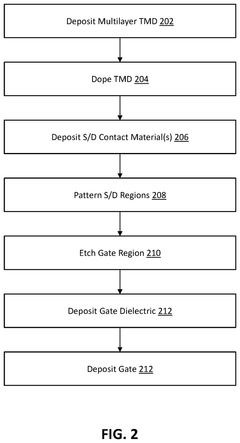
Integrated circuits with monolayer TMD channel and multilayer TMD source and drain
PatentPendingUS20240355934A1
Innovation
- The use of multilayer TMDs with doped upper portions to form monolayer channels, where the upper layers are selectively removed using techniques like atomic layer etching to create a monolayer TMD channel between multilayer source and drain regions, facilitating conductive contacts and reducing defects.


Transition metal dichalcogenides and uses thereof
PatentWO2021015677A1
Innovation
- Surface modification of TMDs with Group 1 metals like Cs and Rb, forming a layer on the surface to achieve a hetero-phase contact between 2H and IT' phases, which reduces contact resistance and enhances electrical properties.
Manufacturing Scalability Assessment
The scalability of TMD-based flexible electronics manufacturing represents a critical challenge for transitioning from laboratory demonstrations to commercial viability. Current production methods for TMDs predominantly rely on chemical vapor deposition (CVD) and mechanical exfoliation techniques, which face significant limitations in terms of throughput, uniformity, and cost-effectiveness at industrial scales. CVD processes can produce high-quality TMD films but typically yield small areas and require precise control of growth parameters, making scale-up challenging.
Solution-based manufacturing approaches, including liquid-phase exfoliation and ink formulations, offer promising pathways for large-area production. These methods enable roll-to-roll processing compatibility, potentially reducing production costs by 60-70% compared to vacuum-based techniques. However, these approaches still struggle with maintaining consistent electronic properties across large substrates, with performance variations often exceeding 25% between batches.
Transfer techniques for integrating TMD films onto flexible substrates present another scalability bottleneck. Current methods often introduce defects, contamination, and mechanical stress that compromise device performance. Recent advancements in polymer-assisted transfer methods have improved yield rates from approximately 40% to 75%, but further optimization is required for industrial implementation.
Equipment standardization remains underdeveloped, with most TMD manufacturing relying on customized research-grade tools rather than industrial production systems. This lack of standardized equipment contributes to reproducibility challenges and increases capital investment requirements, with current estimates suggesting that establishing a production line requires 3-5 times the investment compared to conventional thin-film electronics manufacturing.
Material supply chain considerations further complicate scalability. The availability of high-purity precursors for TMD synthesis is limited, with current global production capacity estimated at less than 100 kg annually for electronics-grade materials. This supply constraint creates potential bottlenecks for large-scale manufacturing and contributes to high material costs, currently averaging $5,000-10,000 per kilogram.
Recent industry-academic collaborations have demonstrated promising advances, with pilot production lines achieving throughput rates of approximately 0.5-1 m²/hour for flexible TMD-based devices. While this represents significant progress, it remains 1-2 orders of magnitude below the production rates required for cost-competitive manufacturing. Achieving economically viable production will require continued innovation in synthesis methods, transfer techniques, and equipment design, with particular emphasis on maintaining mechanical robustness throughout the manufacturing process.
Environmental Impact and Sustainability
The environmental implications of TMD-based flexible electronics represent a critical dimension that must be thoroughly evaluated as this technology advances toward widespread commercial adoption. The extraction and processing of transition metal dichalcogenides (TMDs) like MoS2, WS2, and WSe2 involve mining activities that can lead to habitat disruption, water pollution, and energy-intensive refinement processes. However, compared to traditional silicon-based electronics manufacturing, TMD production potentially requires fewer toxic chemicals and generates less hazardous waste, offering a comparative environmental advantage.
The ultra-thin nature of TMD materials contributes significantly to resource efficiency, as these atomically thin layers require substantially less raw material than conventional semiconductor technologies. This material efficiency translates directly to reduced environmental footprint throughout the supply chain, from extraction to manufacturing. Additionally, the mechanical flexibility and durability of TMD-based devices potentially extend product lifespans, reducing electronic waste generation that currently poses a significant global environmental challenge.
Energy consumption during device operation represents another important sustainability consideration. TMD-based flexible electronics typically operate at lower voltages and demonstrate improved energy efficiency compared to rigid silicon counterparts, potentially reducing the carbon footprint associated with device usage. This efficiency becomes particularly significant when considering the proliferation of Internet of Things (IoT) devices and wearable technologies that require continuous power.
End-of-life management presents both challenges and opportunities for TMD-based flexible electronics. The composite nature of flexible devices—combining TMD materials with polymer substrates and various metals—complicates recycling processes. However, research into delamination techniques and selective material recovery shows promise for establishing closed-loop systems that could significantly reduce waste and recover valuable materials.
Biodegradable substrate integration represents a promising frontier for enhancing the sustainability profile of TMD-based flexible electronics. Recent research demonstrates successful integration of TMDs with biodegradable polymers and cellulose-based materials, potentially enabling electronics that can decompose safely after their useful life. This approach could revolutionize electronic waste management, particularly for short-lifespan applications like disposable medical sensors or temporary environmental monitors.
Regulatory frameworks worldwide are increasingly emphasizing extended producer responsibility and circular economy principles for electronics. TMD-based flexible electronics manufacturers must proactively address these sustainability considerations through design for disassembly, material selection optimization, and development of take-back programs to ensure compliance with evolving environmental regulations while meeting market expectations for responsible production.
Unlock deeper insights with PatSnap Eureka Quick Research — get a full tech report to explore trends and direct your research. Try now!
Generate Your Research Report Instantly with AI Agent
Supercharge your innovation with PatSnap Eureka AI Agent Platform!