How to Optimize Contact Resistance in TMD-Based Transistors
AUG 27, 202510 MIN READ
Generate Your Research Report Instantly with AI Agent
Patsnap Eureka helps you evaluate technical feasibility & market potential.
TMD Transistor Contact Resistance Background and Objectives
Transition metal dichalcogenides (TMDs) have emerged as promising materials for next-generation electronic devices due to their unique two-dimensional structure and exceptional electronic properties. Since the successful isolation of graphene in 2004, the exploration of 2D materials has expanded significantly, with TMDs gaining particular attention for semiconductor applications. These atomically thin materials, with their formula MX2 (where M represents transition metals like Mo, W, and X represents chalcogens like S, Se, Te), exhibit direct bandgaps in the monolayer form, making them ideal candidates for transistor applications.
The evolution of TMD-based transistors has been marked by significant advancements in material synthesis, device fabrication, and performance optimization. However, contact resistance remains a persistent challenge that severely limits device performance and practical applications. This technical bottleneck has become increasingly critical as device dimensions continue to shrink according to Moore's Law, with contact resistance becoming a dominant factor in overall device resistance.
The primary objective of this technical research is to comprehensively investigate and develop innovative approaches to minimize contact resistance in TMD-based transistors. This involves understanding the fundamental mechanisms of carrier transport at metal-TMD interfaces, identifying the key factors contributing to high contact resistance, and exploring novel materials and engineering techniques to overcome these limitations.
Current research indicates that contact resistance in TMD transistors is typically orders of magnitude higher than in conventional silicon devices, with values often exceeding 1 kΩ·μm. This high resistance significantly degrades key performance metrics including on-current, transconductance, and switching speed. The International Roadmap for Devices and Systems (IRDS) has identified contact resistance reduction as a critical requirement for the commercial viability of TMD-based electronics.
The technical goals of this research include: achieving contact resistance values below 100 Ω·μm for practical applications; developing scalable and CMOS-compatible contact engineering methods; establishing reliable and reproducible fabrication processes; and creating comprehensive models to predict and optimize metal-TMD interfaces.
This investigation will build upon recent breakthroughs in contact engineering strategies, including phase engineering of TMDs, insertion of work function engineering layers, doping techniques, and edge contact approaches. By systematically analyzing these methods and exploring their combinations, we aim to establish a clear technological pathway toward ultra-low contact resistance in TMD transistors.
The successful optimization of contact resistance will not only enhance the performance of individual TMD transistors but also enable their integration into complex circuits and systems, potentially revolutionizing applications in flexible electronics, ultra-low power computing, and beyond-CMOS technologies.
Market Analysis for Low-Resistance TMD Transistors
The global market for TMD-based transistors with optimized contact resistance is experiencing significant growth, driven by increasing demand for high-performance, energy-efficient electronic devices. Current market valuations indicate that the semiconductor industry segment focused on next-generation transistor technologies is expanding at a compound annual growth rate of approximately 18% through 2028, with TMD-based solutions gaining substantial market share.
Consumer electronics represents the largest application segment for low-resistance TMD transistors, accounting for nearly 40% of the total addressable market. This is primarily due to the growing consumer preference for devices with longer battery life and faster processing capabilities. The miniaturization trend in smartphones, tablets, and wearable technology has created a strong demand for transistors that can maintain performance while reducing power consumption.
The automotive sector presents another rapidly expanding market opportunity, particularly with the accelerating adoption of electric vehicles and advanced driver-assistance systems. These applications require transistors capable of handling higher power loads while maintaining efficiency, creating a premium segment where optimized TMD transistors can command higher margins.
Industrial IoT applications constitute a growing market segment with projected annual growth exceeding 25% over the next five years. The deployment of edge computing devices and sensors in industrial environments demands transistors with superior reliability and performance characteristics that TMD-based solutions can potentially deliver.
Market research indicates that customers are willing to pay a premium of up to 30% for transistor technologies that can demonstrate significant improvements in power efficiency and performance. This price elasticity creates favorable conditions for the commercialization of advanced TMD transistor technologies with optimized contact resistance.
Regional analysis shows that East Asia continues to dominate the market with approximately 65% share of production capacity, though North America leads in research innovation and intellectual property development. Europe is emerging as a significant market player through targeted investments in quantum computing and advanced electronics manufacturing.
The competitive landscape reveals increasing collaboration between academic institutions and industry partners, with over 200 research partnerships formed in the past three years specifically focused on contact resistance optimization in 2D materials. This trend indicates growing commercial interest and market readiness for TMD transistor technologies.
Market barriers include high initial manufacturing costs and integration challenges with existing semiconductor fabrication processes. However, the potential performance benefits are driving substantial investment in manufacturing scale-up, with dedicated production lines being established by major semiconductor manufacturers.
Current Challenges in TMD Contact Engineering
Despite significant advancements in TMD-based transistors, contact engineering remains one of the most critical challenges hindering their commercial viability. The fundamental issue stems from the formation of Schottky barriers at metal-TMD interfaces, which substantially increases contact resistance. This barrier formation is primarily attributed to Fermi level pinning effects, where the metal work function becomes less influential in determining the barrier height due to interface states.
The atomically thin nature of TMD materials presents unique challenges not encountered in conventional semiconductor technologies. The absence of dangling bonds on pristine TMD surfaces makes it difficult to form strong chemical bonds with contact metals, resulting in weak physical adsorption that impedes efficient carrier injection. Furthermore, the large bandgap of most TMDs (1-2 eV) inherently contributes to significant contact resistance.
Current fabrication processes introduce additional complications. Exposure to ambient conditions during device fabrication leads to unavoidable contamination and oxidation of TMD surfaces. High-temperature processes can cause degradation of TMD properties, while conventional lithography techniques often leave polymer residues that further deteriorate contact quality. The ultra-thin nature of TMDs also makes them highly susceptible to damage during metal deposition processes.
Another significant challenge is the anisotropic carrier transport in TMDs. The in-plane conductivity significantly exceeds the out-of-plane conductivity, creating a bottleneck for vertical carrier transport at contacts. This anisotropy necessitates specialized contact geometries that can effectively leverage the superior in-plane transport properties.
The lack of standardized contact resistance measurement methodologies specifically tailored for 2D materials further complicates progress in this field. Traditional techniques like the transfer length method (TLM) require adaptation for the unique properties of TMDs, leading to inconsistencies in reported values across research groups.
Material quality and homogeneity issues also contribute to contact engineering challenges. Variations in layer thickness, defect density, and grain boundaries significantly impact contact properties, making it difficult to achieve reproducible results. The presence of chalcogen vacancies, particularly prevalent at TMD edges, creates localized states that unpredictably alter contact behavior.
Scalability remains a persistent obstacle, as techniques that demonstrate excellent contact properties in laboratory settings often prove incompatible with large-scale manufacturing processes. Methods like edge contacts or phase engineering show promising results but face significant implementation barriers in industrial production environments.
State-of-the-Art Contact Resistance Solutions
01 Contact materials for TMD-based transistors
The choice of contact materials significantly impacts the contact resistance in TMD-based transistors. Various metals and alloys can be used to form electrical contacts with transition metal dichalcogenide (TMD) layers. Materials with appropriate work functions that match the electronic properties of TMDs can reduce Schottky barrier heights and minimize contact resistance. Some approaches include using low work function metals for n-type contacts and high work function metals for p-type contacts to TMD semiconductors.- Materials for reducing contact resistance in TMD transistors: Various materials can be used to reduce contact resistance in TMD-based transistors. These include metal contacts with specific work functions, transition metal carbides, and other specialized contact materials that form low-resistance interfaces with TMD layers. The selection of appropriate contact materials is crucial for optimizing the electrical performance of TMD transistors by minimizing the Schottky barrier height and improving carrier injection.
- Contact engineering techniques for TMD transistors: Various engineering techniques can be applied to reduce contact resistance in TMD-based transistors. These include interface doping, edge contact formation, phase engineering of TMDs at contact regions, and creation of heterojunctions. These approaches modify the interface between the contact material and the TMD layer to facilitate better carrier transport across the junction, thereby reducing the overall contact resistance.
- Structural modifications to reduce contact resistance: Structural modifications to TMD-based transistors can significantly reduce contact resistance. These include creating overlapping gate structures, implementing recessed contacts, using multi-layer contact architectures, and optimizing the geometry of contact regions. By carefully designing the physical structure of the contacts and their integration with the TMD channel, the resistance at the metal-semiconductor interface can be minimized.
- Thermal and chemical treatment methods: Thermal and chemical treatments can be applied to reduce contact resistance in TMD-based transistors. These include annealing processes, surface functionalization, chemical doping of contact regions, and plasma treatments. These methods modify the chemical composition and electronic properties of the TMD surface at the contact interface, leading to improved carrier injection and reduced contact resistance.
- Advanced fabrication techniques for low-resistance contacts: Advanced fabrication techniques can be employed to create low-resistance contacts for TMD-based transistors. These include selective area growth of contacts, van der Waals epitaxy, atomic layer deposition of interface layers, and clean transfer methods. These fabrication approaches enable the creation of atomically clean interfaces between the contact materials and TMD layers, minimizing defects and contaminants that contribute to contact resistance.
02 Interface engineering techniques
Interface engineering between the metal contacts and TMD layers is crucial for reducing contact resistance. Techniques include surface treatments, insertion of buffer layers, and doping of contact regions. These methods modify the interface properties to improve carrier injection and extraction. By controlling the interface chemistry and structure, the formation of unwanted interfacial layers can be prevented, and the electronic coupling between the metal and TMD can be enhanced, leading to lower contact resistance.Expand Specific Solutions03 Edge contact and phase engineering
Edge contact strategies involve making electrical connections to the edges of TMD layers rather than the surface, which can significantly reduce contact resistance by accessing the conduction channel directly. Phase engineering involves creating metallic phases of TMDs at contact regions while maintaining semiconducting properties in the channel region. This approach creates a seamless interface between metallic and semiconducting regions of the same material, minimizing resistance at the junction.Expand Specific Solutions04 Thermal and pressure-assisted contact formation
Thermal annealing and pressure-assisted techniques can improve contact quality in TMD-based transistors. These processes enhance the metal-TMD interface by promoting diffusion, reducing interfacial contamination, and improving adhesion. Controlled annealing temperatures and environments can optimize the contact formation without damaging the TMD layers. Pressure-assisted methods can ensure better physical contact between metals and TMDs, reducing air gaps and contact resistance.Expand Specific Solutions05 Novel contact architectures and 2D material heterostructures
Advanced contact architectures, including recessed contacts, overlapped contacts, and embedded contacts, can be employed to reduce contact resistance in TMD transistors. Additionally, using other 2D materials as contact interlayers between metals and TMDs can provide better electronic coupling. Graphene and other 2D materials can serve as effective contact materials or buffer layers due to their unique electronic properties and atomically thin nature, facilitating efficient carrier transport across the metal-TMD interface.Expand Specific Solutions
Leading Research Groups and Companies in TMD Electronics
The TMD-based transistor contact resistance optimization landscape is currently in a growth phase, with the market expanding due to increasing demand for high-performance, energy-efficient electronics. The global market is projected to reach significant scale as 2D materials gain commercial traction. Technologically, the field is transitioning from research to early commercialization, with varying maturity levels across players. Intel, Samsung, and TSMC lead with advanced manufacturing capabilities and significant R&D investments. Applied Materials and GlobalFoundries provide critical fabrication technologies, while research institutions like CEA and Tohoku University contribute fundamental innovations. Chinese companies including Huawei and emerging players like Jingxincheng are rapidly advancing their capabilities, creating a competitive environment where collaboration between academia and industry is driving progress toward practical implementation.
Intel Corp.
Technical Solution: Intel has developed a comprehensive approach to optimize contact resistance in TMD-based transistors through their advanced materials engineering. Their solution involves using phase-engineered contacts where they locally convert the semiconductor phase of TMDs to metallic phases at contact regions. This technique creates a seamless interface between the metal contacts and the TMD channel, significantly reducing the Schottky barrier height. Intel's researchers have also implemented work function engineering by introducing interlayers between the metal and TMD to tune the band alignment. Additionally, they've pioneered doping techniques specific to TMDs that create highly doped regions under contacts without damaging the atomically thin materials. Their process integrates these approaches with advanced deposition methods that ensure clean interfaces and minimal damage during fabrication.
Strengths: Intel's approach benefits from their advanced semiconductor fabrication infrastructure, allowing for precise control of interfaces at atomic scales. Their solution is highly compatible with existing CMOS processes, facilitating integration into current manufacturing lines. Weaknesses: The phase engineering process requires precise temperature control that may be challenging to maintain uniformly across large wafers, potentially affecting yield in mass production.
Samsung Electronics Co., Ltd.
Technical Solution: Samsung has developed a multi-faceted approach to contact resistance optimization in TMD transistors focusing on edge contact technology. Their solution involves creating edge contacts to TMD layers rather than traditional top contacts, exposing the edges of TMD layers through precise etching processes. This approach significantly increases the contact area and reduces the tunneling barrier. Samsung's researchers have implemented a proprietary metal stack technology that uses multiple metals with carefully engineered work functions to create optimal band alignment with TMDs. They've also developed a pre-contact treatment process using plasma functionalization that modifies the TMD surface chemistry before metal deposition, creating stronger chemical bonds between the contact metal and TMD material. Their approach includes post-deposition annealing steps performed in controlled environments to further reduce interface states and improve contact quality.
Strengths: Samsung's edge contact approach addresses the fundamental challenge of van der Waals gaps between metals and TMD surfaces, achieving significantly lower contact resistance compared to conventional methods. Their integration of this technology with their advanced semiconductor manufacturing capabilities enables rapid commercialization pathways. Weaknesses: The edge contact fabrication requires extremely precise etching control that adds complexity to the manufacturing process and may impact device-to-device consistency.
Key Patents and Publications on TMD Contact Engineering
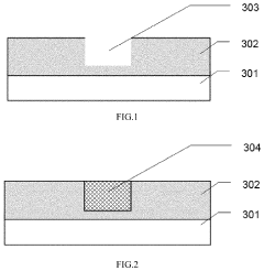
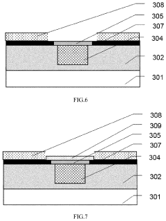
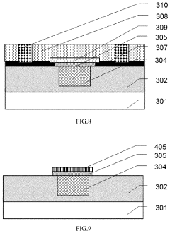
Transition metal dichalcogenide transistor and preparation method thereof
PatentActiveUS20210408296A1
Innovation
- A transition metal dichalcogenide transistor design with a metallic source/drain region and a semiconductor channel layer, where the source/drain regions are formed using first transition metal dichalcogenides like MoTe2, MoS2, and WTe2, and the channel layer is formed using second transition metal dichalcogenides like MoTe2, MoSe2, WSe2, ReSe2, TaS2, TaSe2, TaTe2, NbS2, NbSe2, and NbTe2, ensuring compatibility with existing CMOS processes through a specific layering and doping process.

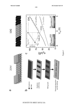
Apparatuses with atomically-thin ohmic edge contacts between two-dimensional materials, methods of making same, and devices comprising same
PatentWO2017218488A1
Innovation
- The development of atomically-thin ohmic edge contacts between monolayer graphene and TMDs, where a single-layer TMD is grown only on the substrate and lateral edges of the graphene film, using a scalable and controllable growth method to achieve low contact resistance and minimal electrode volume, maintaining ohmic behavior down to liquid helium temperatures.


Materials Compatibility and Integration Strategies
The compatibility of contact materials with TMD semiconductors represents a critical factor in optimizing contact resistance. Traditional metal contacts such as gold, titanium, and nickel often form Schottky barriers with TMDs due to Fermi level pinning effects, resulting in high contact resistance. Recent research has demonstrated that phase-engineered contacts, where localized regions of the TMD are transformed from semiconducting to metallic phases, can significantly reduce contact resistance by creating seamless interfaces between the metal and semiconductor regions.
Integration strategies must consider the thermal budget constraints of TMD materials, as excessive temperatures during processing can degrade their electronic properties. Low-temperature deposition techniques such as electron beam evaporation and sputtering at optimized conditions have shown promise for preserving TMD integrity while achieving good contact formation. Additionally, the development of edge contacts rather than top contacts has emerged as an effective approach, as they access the conduction band directly at the TMD edges, bypassing the van der Waals gap that typically impedes carrier injection.
Surface preparation protocols prior to contact deposition significantly impact contact resistance. Controlled surface functionalization using plasma treatments or chemical methods can modify the TMD surface energy and improve metal adhesion. However, these treatments must be carefully calibrated to avoid introducing defects that could degrade device performance. The use of buffer layers between metals and TMDs, such as transition metal oxides or 2D materials like graphene, has demonstrated effectiveness in mitigating Fermi level pinning and enhancing carrier injection.
Encapsulation strategies using hexagonal boron nitride (h-BN) or high-k dielectrics have shown dual benefits of protecting TMD channels from environmental degradation while simultaneously improving contact interfaces. These encapsulation approaches must be integrated early in the fabrication process flow to maximize their effectiveness without compromising contact quality.
The scalability of contact formation techniques represents a significant challenge for industrial adoption. While techniques like transfer-free growth of contacts show excellent performance in laboratory settings, their compatibility with large-scale manufacturing processes remains limited. Recent advances in selective area growth and lithography-compatible deposition methods offer promising pathways toward scalable integration of low-resistance contacts in TMD-based transistors.
Heterogeneous integration with silicon CMOS platforms requires careful consideration of thermal budgets, chemical compatibility, and process contamination. The development of back-end-of-line compatible processes for TMD contact formation, operating below 400°C, has become a key focus area for enabling practical applications in hybrid electronic systems.
Scalability and Manufacturing Considerations
The scalability of TMD-based transistors from laboratory prototypes to industrial-scale manufacturing represents a critical challenge in commercializing this promising technology. Current fabrication methods for TMD-based devices often rely on mechanical exfoliation or chemical vapor deposition (CVD) techniques that produce high-quality materials but face significant limitations in terms of throughput, uniformity, and cost-effectiveness at scale.
Large-area synthesis of TMD materials with consistent properties remains problematic, with variations in layer thickness, defect density, and grain boundaries significantly affecting contact resistance performance. Recent advancements in metal-organic chemical vapor deposition (MOCVD) and atomic layer deposition (ALD) show promise for producing uniform TMD films across larger substrates, potentially enabling wafer-scale integration compatible with existing semiconductor manufacturing infrastructure.
Contact formation processes present additional manufacturing challenges. High-temperature annealing steps commonly used to improve contact interfaces may not be compatible with back-end-of-line (BEOL) processing in integrated circuits. Alternative approaches using low-temperature plasma treatments or selective area growth of contacts require further development to ensure reliability and reproducibility in high-volume manufacturing environments.
Integration with conventional CMOS processes represents another significant hurdle. The thermal budget constraints, material compatibility issues, and process contamination risks must be carefully managed when introducing TMD materials into established semiconductor fabrication lines. Several research groups have demonstrated promising results using modified process flows that maintain TMD material integrity while achieving CMOS compatibility.
Metrology and quality control systems for TMD-based devices require substantial development. Current techniques for measuring contact resistance in research settings often involve complex, time-consuming procedures unsuitable for production environments. Automated, non-destructive testing methods capable of rapidly characterizing contact properties across entire wafers will be essential for viable manufacturing.
Economic considerations also play a crucial role in scalability. The cost structure of TMD-based transistor production must approach that of conventional silicon technology to justify adoption. This includes not only material costs but also equipment investments, process complexity, and yield management. Preliminary cost models suggest that achieving competitive pricing will require significant advances in synthesis techniques and process simplification.
Environmental stability and device encapsulation present additional manufacturing challenges. TMD materials are known to be sensitive to ambient conditions, with oxidation and moisture affecting device performance over time. Developing cost-effective, manufacturing-friendly encapsulation techniques that preserve optimal contact properties will be critical for ensuring long-term reliability in commercial applications.
Unlock deeper insights with Patsnap Eureka Quick Research — get a full tech report to explore trends and direct your research. Try now!
Generate Your Research Report Instantly with AI Agent
Supercharge your innovation with Patsnap Eureka AI Agent Platform!