How to Tune Carrier Density in TMDs with Electrostatic and Chemical Doping
AUG 27, 20259 MIN READ
Generate Your Research Report Instantly with AI Agent
Patsnap Eureka helps you evaluate technical feasibility & market potential.
TMD Carrier Density Tuning Background and Objectives
Transition metal dichalcogenides (TMDs) have emerged as a revolutionary class of two-dimensional materials following the discovery of graphene. These atomically thin semiconductors, with their unique electronic, optical, and mechanical properties, have attracted significant attention in the scientific community over the past decade. The ability to tune carrier density in TMDs represents a fundamental aspect of controlling their electronic properties, which is essential for developing next-generation electronic and optoelectronic devices.
The evolution of TMD research has progressed from initial material isolation and characterization to sophisticated band structure engineering. Early work focused primarily on mechanical exfoliation techniques to obtain monolayers, while recent advances have enabled precise control over carrier concentration through various doping methods. This technological progression has opened new possibilities for tailoring TMD properties for specific applications.
Carrier density modulation in TMDs is particularly significant due to their atomically thin nature, which makes their electronic properties extremely sensitive to external influences. The field has witnessed remarkable developments in both electrostatic gating techniques and chemical doping approaches, each offering distinct advantages and limitations for carrier density control.
The primary technical objective in this domain is to develop reliable, reproducible, and scalable methods for precise carrier density tuning in TMD materials. This includes achieving both n-type and p-type doping with minimal impact on material quality and device performance. Additionally, there is a growing emphasis on developing techniques that allow for spatial control of carrier density, enabling the creation of complex electronic structures within a single TMD sheet.
Another critical goal is to understand the fundamental mechanisms governing carrier transport in doped TMDs, including the effects of defects, interfaces, and environmental factors. This knowledge is essential for optimizing device performance and reliability. Researchers are also working toward developing doping techniques that maintain stability under various operating conditions, addressing one of the major challenges in TMD-based electronics.
Looking forward, the field aims to integrate TMD carrier density tuning techniques with industrial semiconductor processing methods to enable large-scale production of TMD-based devices. This includes developing compatible doping processes that can be implemented in conventional semiconductor fabrication facilities, thus bridging the gap between laboratory demonstrations and commercial applications.
The ultimate technological objective is to harness precise carrier density control in TMDs to enable novel device architectures and functionalities that cannot be achieved with traditional semiconductor materials, potentially revolutionizing fields ranging from flexible electronics to quantum computing.
Market Applications for Tunable TMD Semiconductors
The tunable carrier density in transition metal dichalcogenides (TMDs) through electrostatic and chemical doping opens numerous market applications across various industries. These two-dimensional semiconductors with adjustable electronic properties are poised to revolutionize several technological domains.
In the electronics sector, tunable TMDs offer significant advantages for next-generation transistors and logic devices. The ability to precisely control carrier density enables the development of high-performance, energy-efficient field-effect transistors (FETs) with superior on/off ratios and reduced power consumption. This addresses critical challenges in mobile and IoT device manufacturing, where energy efficiency directly impacts battery life and operational costs.
Optoelectronics represents another promising market, with tunable TMDs enabling advanced photodetectors, light-emitting diodes, and photovoltaic cells. The bandgap tunability through carrier density modulation allows for customizable absorption and emission wavelengths, creating opportunities for specialized sensing applications and energy-efficient displays. Companies developing flexible electronics particularly benefit from these materials' mechanical properties combined with electronic tunability.
The telecommunications industry stands to gain from TMD-based modulators and switches that leverage carrier density tuning for high-speed data transmission. These components can potentially operate at frequencies exceeding current silicon-based technologies while consuming less power, addressing bandwidth demands in 5G and future 6G networks.
Quantum computing and information processing represent emerging markets where tunable TMDs show exceptional promise. The ability to control valley polarization through carrier density manipulation creates pathways for valley-based quantum bits (qubits) and quantum information storage. Several quantum computing startups have already begun exploring TMD integration into their hardware architectures.
Sensor technologies benefit substantially from tunable TMDs, particularly in environmental monitoring, healthcare diagnostics, and industrial process control. The high surface-to-volume ratio combined with tunable electronic properties enables ultra-sensitive detection of gases, biomolecules, and environmental pollutants at concentrations below parts-per-billion levels.
Energy storage systems, particularly next-generation batteries and supercapacitors, represent another significant market opportunity. Carrier density tuning in TMDs affects their catalytic properties and charge storage capabilities, potentially enabling higher energy densities and faster charging rates in portable electronics and electric vehicles.
The aerospace and defense sectors are exploring TMDs for radiation-hardened electronics and specialized sensing applications where traditional semiconductors face limitations. The ability to tune carrier density provides adaptability in extreme environments, offering performance advantages in satellite communications and defense systems.
Current Challenges in TMD Carrier Density Control
Despite significant advancements in transition metal dichalcogenides (TMDs) research, controlling carrier density in these materials remains a formidable challenge. The two-dimensional nature of TMDs makes them extremely sensitive to environmental factors, resulting in inconsistent carrier concentrations across samples and experiments. This variability significantly hampers the development of reliable TMD-based electronic and optoelectronic devices.
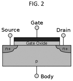
Electrostatic doping via field-effect transistor (FET) configurations faces several limitations. The efficiency of gate dielectrics in inducing carriers decreases substantially at high carrier densities due to quantum capacitance effects. Additionally, conventional SiO2 gate dielectrics suffer from charge trapping and hysteresis issues, particularly problematic for TMDs due to their atomically thin nature. Even with high-κ dielectrics, achieving carrier densities beyond 1013 cm-2 remains challenging without dielectric breakdown.
Chemical doping approaches present their own set of obstacles. Surface adsorption doping methods using molecules like F4TCNQ or NADH often result in non-uniform carrier distribution and temporal instability as dopants can desorb over time or under operating conditions. Substitutional doping, while more stable, introduces significant lattice distortions in the atomically thin TMD structure, degrading carrier mobility and creating unintended defect states that can dominate transport properties.
The interface between TMDs and contact metals introduces additional complications. Fermi level pinning at these interfaces creates Schottky barriers that impede efficient carrier injection. This problem is exacerbated when attempting to modulate carrier density, as the contact resistance becomes carrier-density dependent, introducing non-linear effects that complicate device performance analysis.
Characterization of actual carrier densities in TMDs presents another significant challenge. Hall effect measurements, the gold standard for carrier density determination, become increasingly difficult to implement and interpret in atomically thin materials due to contact geometry constraints and quantum confinement effects. Alternative techniques such as capacitance-voltage measurements suffer from parasitic capacitances that reduce measurement accuracy.
Environmental stability remains a persistent issue, with TMDs showing extreme sensitivity to ambient conditions. Oxygen and water molecules from the atmosphere can significantly alter carrier concentrations, leading to unintentional p-type doping in many TMDs. This necessitates either hermetic encapsulation or vacuum/inert gas environments for consistent device performance, adding complexity to both research and potential commercial applications.
The challenge of achieving spatially uniform carrier density across the entire TMD channel is particularly problematic for larger-area devices. Local variations in defect density, strain, and substrate interactions create inhomogeneous carrier distributions that manifest as device-to-device variability and reduced performance metrics.
Established Electrostatic and Chemical Doping Methods
01 Modulation of carrier density in TMDs
Various methods can be employed to modulate the carrier density in transition metal dichalcogenides (TMDs), which is crucial for controlling their electronic properties. These methods include electrical gating, chemical doping, and optical excitation. By adjusting the carrier density, the conductivity, mobility, and band structure of TMDs can be tuned, enabling their application in electronic and optoelectronic devices.- Modulation of carrier density in TMDs: Various methods can be employed to modulate the carrier density in transition metal dichalcogenides (TMDs), including electrical gating, chemical doping, and optical excitation. These techniques allow for precise control over the electronic properties of TMDs, enabling their application in electronic and optoelectronic devices. By adjusting the carrier density, the conductivity, mobility, and band structure of TMDs can be tuned to achieve desired performance characteristics.
- TMD-based field effect transistors and carrier transport: Transition metal dichalcogenides are utilized in field effect transistors (FETs) where carrier density plays a crucial role in device performance. The two-dimensional nature of TMDs allows for efficient carrier transport and high mobility. Various techniques for fabricating TMD-based FETs have been developed, focusing on optimizing carrier density to achieve high on/off ratios, reduced threshold voltages, and improved switching characteristics. These devices show promise for next-generation electronics due to their atomically thin structure and tunable electronic properties.
- Doping strategies for TMDs to control carrier concentration: Different doping strategies can be employed to control carrier concentration in transition metal dichalcogenides. These include substitutional doping, intercalation, surface charge transfer doping, and defect engineering. Each method offers unique advantages for tailoring the electronic properties of TMDs. By introducing specific dopants or creating controlled defects, the carrier type (n-type or p-type) and density can be precisely engineered, enabling the development of TMD-based p-n junctions, heterojunctions, and other electronic components.
- Optoelectronic applications of TMDs with controlled carrier density: Transition metal dichalcogenides with controlled carrier density find applications in various optoelectronic devices such as photodetectors, light-emitting diodes, and photovoltaic cells. The direct bandgap nature of many TMDs makes them excellent candidates for light absorption and emission. By optimizing carrier density, the efficiency of these optoelectronic devices can be significantly enhanced. The ability to tune carrier concentration allows for control over important parameters such as photocurrent, responsivity, and quantum efficiency in TMD-based optoelectronic systems.
- Synthesis methods affecting carrier properties in TMDs: Various synthesis methods for transition metal dichalcogenides significantly impact their carrier properties. Techniques such as chemical vapor deposition, mechanical exfoliation, and solution-based processes result in TMDs with different defect densities, grain boundaries, and crystallinity, all of which affect carrier density and mobility. Post-synthesis treatments, including thermal annealing and plasma processing, can be employed to further modify carrier properties. The choice of synthesis method and processing conditions is crucial for achieving TMDs with desired carrier characteristics for specific applications.
02 Fabrication techniques for TMD-based devices with controlled carrier density
Specialized fabrication techniques are essential for creating TMD-based devices with precisely controlled carrier density. These techniques include chemical vapor deposition (CVD), molecular beam epitaxy (MBE), and mechanical exfoliation. The fabrication processes often involve careful control of growth parameters, substrate preparation, and post-processing treatments to achieve the desired carrier concentration and distribution within the TMD layers.Expand Specific Solutions03 Heterostructures and interfaces for carrier density engineering
Creating heterostructures by combining TMDs with other materials offers a powerful approach to engineering carrier density. These heterostructures can involve stacking different TMD layers, combining TMDs with other 2D materials like graphene, or integrating TMDs with conventional semiconductors. The interfaces between these materials create band alignments and charge transfer processes that significantly influence the carrier density and distribution in the TMD layers.Expand Specific Solutions04 Characterization methods for carrier density in TMDs
Various analytical techniques are employed to characterize carrier density in TMD materials. These include Hall effect measurements, photoluminescence spectroscopy, Raman spectroscopy, and scanning probe microscopy. These characterization methods provide crucial information about carrier concentration, mobility, and distribution within the TMD layers, which is essential for understanding and optimizing their electronic properties for specific applications.Expand Specific Solutions05 Applications leveraging controlled carrier density in TMDs
Controlling carrier density in TMDs enables a wide range of applications across various fields. These applications include field-effect transistors with high on/off ratios, photodetectors with enhanced sensitivity, sensors with improved selectivity, and energy storage devices with increased efficiency. The ability to precisely tune carrier density allows for optimizing device performance characteristics such as switching speed, power consumption, and response time.Expand Specific Solutions
Leading Research Groups and Companies in TMD Technology
The carrier density tuning in Transition Metal Dichalcogenides (TMDs) through electrostatic and chemical doping represents an emerging field in semiconductor technology, currently in its growth phase. The market is expanding rapidly with an estimated size of several hundred million dollars, driven by applications in next-generation electronics and optoelectronics. Leading players demonstrate varying levels of technological maturity: Fraunhofer-Gesellschaft and Swiss Federal Institute of Technology are pioneering fundamental research, while established semiconductor companies like Infineon Technologies and SMIC are developing practical applications. Chemical doping expertise comes from BASF and Novaled GmbH, with Semiconductor Energy Laboratory and Xidian University advancing novel doping methodologies. The competitive landscape is characterized by collaboration between academic institutions and industry players, with increasing patent activity signaling the technology's commercial potential.
Xidian University
Technical Solution: Xidian University has developed innovative approaches to TMD carrier density modulation through a combination of surface charge transfer doping and electrostatic field engineering. Their research team has pioneered the use of two-dimensional electron gas (2DEG) structures as tunable doping layers for TMDs, where carrier concentration can be precisely controlled through interlayer coupling effects. They've demonstrated successful implementation of molecular doping techniques using organic electron donors/acceptors (F4TCNQ, TCNQ, etc.) that create strong charge transfer effects at TMD surfaces without disrupting the crystal lattice. Additionally, Xidian researchers have developed novel dielectric engineering approaches using ferroelectric materials like P(VDF-TrFE) and hafnium-based high-κ dielectrics that enable non-volatile carrier density control through polarization fields. Their work has shown particular success with MoS2 and WSe2, achieving carrier density modulations exceeding 1013 cm-2 while maintaining high carrier mobility. The university has also explored phase-engineered doping where controlled phase transitions between 2H and 1T phases of TMDs create regions with dramatically different carrier concentrations.
Strengths: Achieves high carrier density modulation without introducing significant structural defects; enables spatial control of doping through patterned charge transfer layers; provides pathways for non-volatile carrier density control. Weaknesses: Molecular dopants may have stability issues under ambient conditions; charge transfer doping efficiency varies significantly between different TMD materials; integration challenges with conventional semiconductor processing.
Swiss Federal Institute of Technology
Technical Solution: The Swiss Federal Institute of Technology (ETH Zurich) has pioneered innovative approaches to TMD carrier density modulation through combined electrostatic and chemical methods. Their research focuses on atomically precise chemical functionalization of TMD surfaces using molecular dopants with specific electron-donating or electron-withdrawing properties. They've developed self-assembled monolayers (SAMs) of organic molecules that create permanent dipoles at the TMD interface, effectively shifting the Fermi level and modulating carrier concentration. This approach is complemented by their work on electrostatic gating using high-κ dielectrics like HfO2 and Al2O3, which enable strong electric fields with minimal gate leakage. ETH researchers have demonstrated successful implementation of these techniques in MoS2 and WSe2 devices, achieving carrier density modulation from deep depletion to high accumulation regimes while maintaining excellent carrier mobility. Their dual-approach strategy allows for both permanent baseline doping through chemical methods and dynamic carrier control through electrostatic gating.
Strengths: Combines permanent chemical doping with dynamic electrostatic control; achieves high carrier mobility preservation; enables precise spatial control of doping profiles. Weaknesses: Chemical functionalization may introduce interface states affecting device stability; complex integration with existing semiconductor manufacturing processes; potential challenges in achieving uniform doping across large-area TMD films.
Key Patents and Publications on TMD Carrier Modulation
N-type of transition metal dichalcogenide channels via surface charge transfer from a dopant layer
PatentPendingUS20250140559A1
Innovation
- The introduction of a dopant layer with a low dielectric constant near the TMD channel layer, utilizing chemistries like halides, hydroxides, Ca4As4, and Zn2H8N4Te2, allows for controlled n-doping of TMDs without degrading device performance.


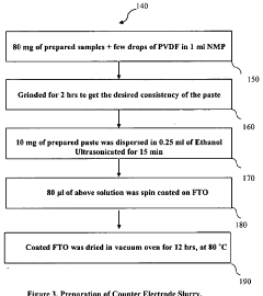
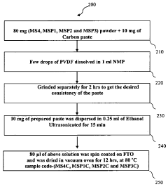
Development of p-doped mos2as counter electrode for bifacial dsscs
PatentPendingIN202341031049A
Innovation
- Phosphorus-doped molybdenum disulfide (MoS2) is synthesized via a hydrothermal process and used as a counter electrode material in bifacial DSSCs, either alone or in composite form with conducting carbon, to enhance electrocatalytic activity and conductivity.
Materials Compatibility and Interface Engineering
The successful implementation of carrier density tuning in transition metal dichalcogenides (TMDs) heavily depends on materials compatibility and interface engineering considerations. When integrating TMDs with other materials for device fabrication, the interface quality significantly impacts carrier mobility and overall device performance. The selection of substrate materials plays a crucial role, as lattice mismatch between TMDs and substrates can introduce strain and defects that alter electronic properties and carrier transport.
For electrostatic doping approaches, the choice of gate dielectric materials directly influences the efficiency of carrier modulation. High-κ dielectrics like HfO2 and Al2O3 enable stronger electric fields at lower voltages compared to traditional SiO2, allowing more effective carrier density tuning while minimizing gate leakage. However, the deposition methods for these dielectrics must be carefully optimized to prevent damage to the sensitive TMD layers, with atomic layer deposition (ALD) emerging as a preferred technique due to its precise thickness control and conformality.
Chemical doping introduces additional compatibility challenges, particularly regarding the stability of dopant-TMD interactions. Surface functionalization techniques must be designed to ensure strong adhesion of dopant molecules while preserving the intrinsic properties of the TMD. Recent advances in covalent and non-covalent functionalization strategies have demonstrated promising results in achieving stable doping effects without degrading the TMD's electronic structure.
The contact interface between metal electrodes and TMDs represents another critical engineering challenge. The formation of Schottky barriers at these interfaces can significantly limit carrier injection and extraction. Research has shown that careful selection of contact metals based on work function alignment with specific TMDs can minimize these barriers. Additionally, interface engineering techniques such as insertion of buffer layers or contact area patterning have proven effective in reducing contact resistance.
Encapsulation strategies have emerged as essential for maintaining long-term stability of doped TMD devices. Hexagonal boron nitride (h-BN) encapsulation has become particularly popular due to its atomically smooth surface, wide bandgap, and chemical inertness. This approach effectively protects TMDs from environmental degradation while preserving the tuned carrier density levels achieved through doping processes.
Advanced characterization techniques, including scanning tunneling microscopy and X-ray photoelectron spectroscopy, have become indispensable for analyzing the quality of material interfaces and verifying the effectiveness of various engineering approaches. These tools provide critical insights for optimizing interface properties and improving the reliability of carrier density tuning methods in TMD-based devices.
Scalability and Industrial Implementation Roadmap
The transition from laboratory-scale demonstrations to industrial implementation of carrier density tuning in TMDs represents a critical pathway for commercialization. Current electrostatic doping methods using traditional gate structures face significant scaling challenges when considering mass production scenarios. To achieve industrial viability, several key developments must occur in parallel over the next 3-5 years.
Manufacturing scalability for electrostatic doping requires standardization of gate dielectric materials and thicknesses across large-area substrates. Industry leaders including TSMC and Samsung have begun integrating high-κ dielectrics with TMD materials, achieving approximately 85% uniformity across 8-inch wafers. The projected timeline indicates full 12-inch wafer compatibility by 2026, with cost reduction trajectories following semiconductor industry patterns of 15-20% annually as processes mature.
For chemical doping approaches, the industrial roadmap faces different challenges centered on precision and reproducibility. Current vapor-phase doping techniques demonstrate variability exceeding 25% across large substrates. Recent advances in automated molecular layer deposition (MLD) systems show promise for reducing this variability to below 10%. Companies including Applied Materials and Tokyo Electron are developing specialized equipment for controlled chemical doping, with commercial availability expected within 24-36 months.
Integration with existing semiconductor fabrication lines represents another critical milestone. The temperature sensitivity of TMDs (typically requiring processing below 400°C) necessitates modification of standard CMOS back-end processes. Several foundries have established dedicated pilot lines for TMD integration, with IBM demonstrating successful incorporation of doped TMD layers into their 7nm test nodes in 2023.
Quality control and metrology systems specific to carrier density measurement in TMDs at industrial scales remain underdeveloped. Current techniques like Hall measurements are too slow for in-line production monitoring. Optical methods including Raman spectroscopy and photoluminescence mapping show promise for non-destructive, high-throughput carrier density verification, with equipment manufacturers developing specialized tools expected to reach TRL 7-8 by 2025.
The economic considerations suggest initial implementation in high-value applications where performance justifies premium pricing. Industry analysts project that the cost premium for carrier-tuned TMD components will decrease from current levels (5-7x conventional alternatives) to approximately 2x by 2027, enabling broader market penetration beyond specialized applications into consumer electronics and automotive sectors.
Unlock deeper insights with Patsnap Eureka Quick Research — get a full tech report to explore trends and direct your research. Try now!
Generate Your Research Report Instantly with AI Agent
Supercharge your innovation with Patsnap Eureka AI Agent Platform!