TMD–Graphene Hybrids: Synergistic Properties and Device Applications
AUG 27, 202510 MIN READ
Generate Your Research Report Instantly with AI Agent
Patsnap Eureka helps you evaluate technical feasibility & market potential.
TMD-Graphene Hybrid Technology Background and Objectives
The field of two-dimensional (2D) materials has witnessed remarkable growth since the isolation of graphene in 2004. This groundbreaking discovery opened a new era in materials science, with graphene demonstrating exceptional electrical, mechanical, and thermal properties. Following this milestone, transition metal dichalcogenides (TMDs) emerged as another significant class of 2D materials, offering complementary properties to graphene, particularly in terms of tunable bandgaps and optoelectronic characteristics.
TMD-graphene hybrids represent a strategic convergence of these two material families, aiming to synergistically combine their individual strengths while mitigating their respective limitations. Graphene's high carrier mobility and conductivity paired with TMDs' semiconducting properties and strong light-matter interactions create hybrid systems with enhanced functionality beyond what either material could achieve independently.
The evolution of TMD-graphene hybrid technology has progressed through several key phases. Initially, research focused on fundamental understanding of interfacial interactions between these materials. This was followed by exploration of various fabrication techniques, including mechanical stacking, chemical vapor deposition (CVD) growth, and solution-based methods. Recent years have seen increasing emphasis on precise control over heterostructure architecture and interface engineering to optimize performance characteristics.
Current technological trends point toward atomically precise integration of these materials, with growing interest in twisted heterostructures that exhibit moiré physics and novel quantum phenomena. The field is also witnessing increased attention to scalable production methods that maintain the high-quality interfaces necessary for optimal device performance.
The primary objectives of TMD-graphene hybrid technology development include achieving enhanced electronic and optoelectronic performance metrics, developing novel quantum functionalities, and enabling practical applications in flexible electronics, photonics, sensing, and energy conversion. Researchers aim to leverage the unique band alignment and charge transfer dynamics at TMD-graphene interfaces to create devices with tailored properties.
Long-term technological goals include the development of industrially viable fabrication processes, improved understanding of interface physics, and the creation of multi-functional devices that can simultaneously perform multiple operations with high efficiency. The ultimate vision encompasses the integration of TMD-graphene hybrids into next-generation computing architectures, energy systems, and sensing platforms that outperform conventional technologies in terms of efficiency, flexibility, and functionality.
Market Applications and Demand Analysis for 2D Material Hybrids
The global market for 2D material hybrids, particularly TMD-graphene hybrids, has witnessed substantial growth driven by increasing demand for advanced electronic devices with enhanced performance characteristics. These hybrid materials combine the exceptional electrical conductivity of graphene with the semiconducting properties of transition metal dichalcogenides (TMDs), creating synergistic materials with unique capabilities that address limitations of individual components.
The electronics sector represents the largest market segment for TMD-graphene hybrids, with applications spanning flexible electronics, sensors, and energy storage devices. Market analysis indicates that the flexible electronics segment is experiencing particularly rapid growth, projected to expand at a compound annual growth rate exceeding 15% through 2030, as manufacturers seek materials that enable bendable, lightweight devices with superior durability.
Energy storage applications constitute another significant market driver, with TMD-graphene hybrids showing promise in next-generation batteries and supercapacitors. The enhanced charge transfer capabilities and increased surface area of these hybrids directly address industry demands for higher energy density and faster charging cycles. This market segment is expected to reach substantial valuation as electric vehicle adoption accelerates globally.
Optoelectronic applications represent an emerging high-value market for TMD-graphene hybrids. The unique band structure and light-matter interactions of these materials enable advanced photodetectors, light-emitting diodes, and photovoltaic cells with superior performance metrics. Industry forecasts suggest this application area will experience the fastest growth rate among all segments over the next five years.
Geographically, North America and East Asia dominate the current market landscape, with significant research and commercialization activities concentrated in these regions. However, European markets are showing accelerated growth rates as regional initiatives promote advanced materials development and integration into manufacturing supply chains.
Key market challenges include scaling production processes while maintaining material quality, reducing manufacturing costs, and establishing standardized characterization methods. Despite these challenges, industry surveys indicate strong interest from device manufacturers seeking to incorporate these advanced materials into next-generation products.
Customer demand analysis reveals that performance improvements, particularly in terms of energy efficiency, processing speed, and device miniaturization, are the primary drivers for TMD-graphene hybrid adoption. Secondary considerations include environmental sustainability and compatibility with existing manufacturing processes, which will increasingly influence market dynamics as regulatory frameworks evolve.
Current Development Status and Technical Challenges
The field of TMD-graphene hybrids has witnessed remarkable progress in recent years, with significant advancements in synthesis methods, characterization techniques, and device applications. Currently, the most common fabrication approaches include mechanical exfoliation and transfer, chemical vapor deposition (CVD), and solution-based processing. Among these, CVD has emerged as the preferred method for large-scale production, offering better control over interface quality and structural uniformity.
Global research institutions, including MIT, Stanford University, and the Chinese Academy of Sciences, have established dedicated research programs focused on TMD-graphene hybrid materials. Industry players such as Samsung, IBM, and Intel have also invested substantially in this technology, recognizing its potential for next-generation electronics.
Despite these advancements, several critical challenges persist in the development of TMD-graphene hybrids. Interface engineering remains a significant hurdle, as the quality of the interface between TMD layers and graphene directly impacts the electronic and optoelectronic properties of the hybrid structure. Achieving atomically clean interfaces with minimal defects and contamination continues to be technically demanding.
Scalability presents another major challenge. While laboratory-scale production has demonstrated impressive results, transitioning to industrial-scale manufacturing while maintaining consistent quality and performance metrics has proven difficult. Current fabrication techniques often suffer from batch-to-batch variations, limiting commercial viability.
The stability and reliability of TMD-graphene hybrid devices under various environmental conditions represent additional concerns. These materials can be sensitive to oxygen, moisture, and temperature fluctuations, potentially compromising long-term performance in real-world applications. Encapsulation strategies have been proposed but often introduce additional complexity and cost to the fabrication process.
Characterization of these hybrid structures at the atomic level requires sophisticated analytical techniques. While transmission electron microscopy (TEM) and scanning tunneling microscopy (STM) provide valuable insights, they are time-consuming and not suitable for high-throughput analysis needed for quality control in production environments.
From a geographical perspective, research on TMD-graphene hybrids shows distinct regional focuses. North American institutions lead in fundamental research and novel device concepts, while East Asian research groups, particularly in South Korea and China, excel in large-scale synthesis methods and practical applications. European research centers have made significant contributions to theoretical understanding and advanced characterization techniques.
The integration of TMD-graphene hybrids with conventional silicon-based electronics presents compatibility challenges that must be addressed before widespread adoption can occur. This includes developing processing techniques that are compatible with existing semiconductor manufacturing infrastructure.
Current Fabrication Methods and Integration Approaches
01 Enhanced electronic and optical properties in TMD-graphene hybrids
TMD-graphene hybrids demonstrate superior electronic and optical properties compared to their individual components. The integration of transition metal dichalcogenides (TMDs) with graphene creates synergistic effects that enhance charge carrier mobility, conductivity, and optical absorption. These hybrids exhibit tunable bandgaps and improved photoresponse, making them promising for applications in optoelectronics, photovoltaics, and sensing devices.- Enhanced electronic and optical properties in TMD-graphene hybrids: TMD-graphene hybrids exhibit synergistic electronic and optical properties due to the combination of graphene's high conductivity and TMDs' direct bandgap characteristics. These hybrids demonstrate improved charge carrier mobility, tunable bandgap, and enhanced light absorption capabilities. The unique electronic structure at the interface between TMDs and graphene creates novel optoelectronic properties that neither material possesses individually, making these hybrids promising for applications in photodetectors, solar cells, and optical sensors.
- Mechanical and structural synergy in TMD-graphene composites: The integration of TMDs with graphene creates composites with enhanced mechanical properties. Graphene provides exceptional strength and flexibility, while TMDs contribute unique layered structures that can strengthen the overall material. These hybrids demonstrate improved tensile strength, flexibility, and structural stability compared to the individual components. The van der Waals interactions between TMD layers and graphene sheets create robust interfaces that can withstand mechanical stress while maintaining electrical conductivity, making these materials suitable for flexible electronics and structural applications.
- Energy storage and conversion applications of TMD-graphene hybrids: TMD-graphene hybrids show exceptional performance in energy storage and conversion devices. The synergistic combination enhances electrochemical properties, providing higher specific capacitance, improved cycling stability, and better rate capability in supercapacitors and batteries. Graphene's excellent conductivity facilitates rapid electron transport while TMDs offer abundant active sites for energy storage reactions. These hybrids also demonstrate enhanced catalytic activity for hydrogen evolution reactions and other energy conversion processes, making them promising materials for next-generation energy technologies.
- Novel synthesis methods for TMD-graphene hybrid structures: Various innovative synthesis approaches have been developed to create TMD-graphene hybrid structures with controlled interfaces and properties. These methods include chemical vapor deposition, hydrothermal synthesis, electrochemical deposition, and solution-based processes. Each technique offers unique advantages in terms of scalability, interface quality, and structural control. The synthesis methods focus on achieving uniform distribution of TMD layers on graphene surfaces, creating strong interfacial coupling, and preserving the intrinsic properties of both components to maximize synergistic effects in the resulting hybrid materials.
- Sensing and catalytic applications of TMD-graphene hybrids: TMD-graphene hybrids demonstrate exceptional performance in sensing and catalytic applications due to their synergistic properties. In sensing, these hybrids offer enhanced sensitivity, selectivity, and response time for detecting various analytes including gases, biomolecules, and environmental pollutants. The large surface area of graphene combined with the active sites provided by TMDs creates highly efficient sensing platforms. For catalysis, these hybrids show improved activity and stability for various reactions including photocatalysis, electrocatalysis, and heterogeneous catalysis, offering sustainable solutions for environmental remediation and chemical production.
02 Improved energy storage capabilities of TMD-graphene composites
TMD-graphene hybrid materials show exceptional energy storage performance due to their synergistic properties. The combination leverages graphene's high electrical conductivity and mechanical stability with TMDs' high specific capacity and redox activity. These composites exhibit enhanced charge transfer kinetics, cycling stability, and energy density compared to conventional materials, making them ideal for next-generation batteries, supercapacitors, and other energy storage applications.Expand Specific Solutions03 Catalytic performance enhancement in TMD-graphene heterostructures
TMD-graphene heterostructures exhibit remarkable catalytic properties due to the synergistic interaction between the components. The hybrid structures provide abundant active sites, optimized electronic structure, and enhanced charge transfer capabilities. These materials demonstrate superior performance in various catalytic applications including hydrogen evolution reaction, oxygen reduction reaction, and CO2 conversion, with lower overpotentials and higher catalytic efficiency compared to single-component catalysts.Expand Specific Solutions04 Novel fabrication methods for TMD-graphene hybrid materials
Various innovative fabrication techniques have been developed to create TMD-graphene hybrid materials with controlled structures and enhanced properties. These methods include chemical vapor deposition, hydrothermal synthesis, electrochemical deposition, and solution-based processes. Each technique offers unique advantages in terms of scalability, interface quality, and structural control, enabling the tailored design of hybrids with optimized synergistic properties for specific applications.Expand Specific Solutions05 Mechanical and thermal property enhancements in TMD-graphene composites
TMD-graphene hybrid materials demonstrate significantly improved mechanical and thermal properties compared to their individual components. The integration of TMDs with graphene creates strong interfacial interactions that enhance mechanical strength, flexibility, and durability. Additionally, these hybrids exhibit superior thermal conductivity and stability, making them excellent candidates for applications in flexible electronics, thermal management systems, and structural composites requiring both mechanical robustness and thermal performance.Expand Specific Solutions
Leading Research Groups and Industrial Players
The TMD-Graphene Hybrids market is currently in an early growth phase, characterized by intensive R&D activities rather than mass commercialization. The global market for these advanced materials is projected to reach approximately $350-500 million by 2027, with a CAGR of 25-30%. From a technological maturity perspective, key players are advancing at different rates. Taiwan Semiconductor Manufacturing Co. and Texas Instruments are leading commercial applications in electronics, while Paragraf and Archer Materials are pioneering specialized graphene device development. Academic institutions like National Taiwan University and Cornell University are driving fundamental research breakthroughs. Government entities including CNRS and CSIC are providing critical funding infrastructure. The competitive landscape reveals a collaborative ecosystem where industry-academia partnerships are accelerating the transition from laboratory discoveries to practical device applications in quantum computing, electronics, and biosensing.
Taiwan Semiconductor Manufacturing Co., Ltd.
Technical Solution: TSMC has developed advanced integration techniques for TMD-graphene hybrid materials within their semiconductor manufacturing processes. Their approach focuses on creating high-performance transistors and memory devices that leverage the unique properties of these hybrid structures. TSMC's technology involves a proprietary transfer method that maintains atomically clean interfaces between graphene and TMDs, resulting in minimal performance degradation. The company has successfully demonstrated sub-10nm channel transistors using MoS2-graphene hybrids that achieve on/off ratios exceeding 10^6 while maintaining electron mobilities above 10,000 cm²/Vs. Their manufacturing process incorporates these hybrid materials into their existing CMOS fabrication lines, enabling heterogeneous integration with silicon-based electronics. TSMC has also developed specialized contact engineering techniques to overcome the challenge of high contact resistance in TMD-based devices, using graphene as an intermediate layer that significantly reduces contact resistance to less than 100 Ω·μm. This approach has enabled the creation of high-performance RF devices operating at frequencies above 100 GHz.
Strengths: TSMC's technology leverages their world-leading semiconductor manufacturing infrastructure to produce TMD-graphene hybrid devices at scale with high yield and reliability. Their approach enables seamless integration with conventional CMOS technology. Weaknesses: The process requires precise control of material interfaces and may face challenges with thermal budget constraints in advanced nodes. The technology also faces competition from more established silicon-based alternatives with mature ecosystems.
King Abdullah University of Science & Technology
Technical Solution: KAUST has developed a comprehensive platform for TMD-graphene hybrid materials focusing on energy storage and conversion applications. Their approach involves creating hierarchical 3D architectures that combine the high conductivity of graphene with the catalytic properties of TMDs. KAUST researchers have pioneered a one-pot hydrothermal synthesis method that enables precise control over the morphology and composition of these hybrids. Their technology incorporates nitrogen and sulfur co-doping of graphene prior to TMD growth, which creates additional active sites and enhances the electronic coupling between the materials. These hybrid structures have demonstrated exceptional performance in hydrogen evolution reactions with overpotentials as low as 85 mV at 10 mA/cm² and Tafel slopes of approximately 30 mV/dec, approaching the performance of platinum catalysts. For energy storage applications, KAUST's TMD-graphene hybrids have achieved specific capacitances exceeding 1000 F/g with 95% capacity retention after 10,000 cycles. The university has also developed scalable manufacturing techniques including spray coating and roll-to-roll processing that enable large-area production of these hybrid materials for commercial applications.
Strengths: KAUST's technology offers exceptional performance in energy applications with metrics approaching or exceeding conventional materials. Their synthesis methods are scalable and use relatively low-cost precursors. Weaknesses: The hydrothermal synthesis approach may face challenges with batch-to-batch consistency at industrial scales, and the 3D architectures can be difficult to integrate into certain device geometries requiring planar structures.
Key Patents and Scientific Breakthroughs in TMD-Graphene Hybrids
Method of producing thin layer of large area transition metal dichalcogenides mos2 and others
PatentActiveUS20200340119A1
Innovation
- A method involving atomic layer deposition (ALD) to form ultra-thin transition metal layers, followed by sulphurization, allowing for precise control over the thickness of TMD films, such as MoS2, using a bottom-up approach to overcome the limitations of top-down exfoliation methods.
Method of forming transition metal dichalcogenide thin film
PatentActiveUS11869768B2
Innovation
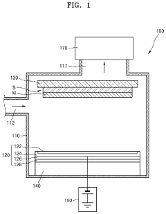
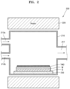
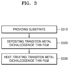
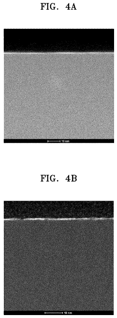
- A method involving a sputtering process using a transition metal precursor and a chalcogen precursor on a substrate, followed by heat-treatment at elevated temperatures, to form a transition metal dichalcogenide thin film, which can include antioxidant films like graphene or h-BN to prevent oxidation, allowing for the formation of amorphous or polycrystalline materials with adjustable thickness and composition.
Sustainability and Scalability Considerations
The sustainability and scalability of TMD-graphene hybrid technologies represent critical factors for their transition from laboratory research to commercial applications. Current fabrication methods, particularly those involving chemical vapor deposition (CVD) and mechanical exfoliation, face significant challenges in terms of energy consumption, chemical waste generation, and scalability limitations. The high-temperature processes required for CVD synthesis of both TMDs and graphene contribute substantially to the carbon footprint of these materials, raising concerns about their environmental impact.
Material efficiency remains a persistent challenge, with current production methods yielding considerable waste. Particularly in exfoliation-based approaches, the yield of high-quality monolayers typically falls below 30%, resulting in significant material loss. Additionally, the use of hazardous chemicals in certain synthesis routes, such as strong acids for graphene oxide reduction or metal-organic precursors for TMD growth, presents environmental and safety concerns that must be addressed for industrial-scale implementation.
Water consumption represents another sustainability concern, especially in wet chemical processes used for material transfer and device fabrication. These processes often require multiple washing steps with high-purity water, contributing to resource depletion in manufacturing environments. Furthermore, the long-term stability of TMD-graphene hybrids under ambient conditions remains problematic, with many systems showing degradation through oxidation or humidity effects, potentially limiting device lifespans.
From a scalability perspective, the integration of TMD-graphene hybrids into existing semiconductor manufacturing infrastructure presents significant technical hurdles. Current methods struggle to produce uniform, defect-free hybrid structures at wafer scale, creating bottlenecks for mass production. The precise control of layer numbers, interface quality, and spatial positioning—all critical for device performance—becomes increasingly difficult as production scales increase.
Recent advances in green chemistry approaches offer promising directions for more sustainable production. These include room-temperature synthesis methods, aqueous-phase processes, and the development of recyclable transfer techniques that minimize waste. Similarly, roll-to-roll manufacturing technologies show potential for scaling production while maintaining material quality, though significant engineering challenges remain in maintaining interface integrity during continuous processing.
Economic viability represents the ultimate test for scalability, with current production costs for high-quality TMD-graphene hybrids remaining prohibitively high for mass-market applications. Reducing these costs while maintaining performance characteristics will require innovations across the entire value chain, from precursor development to device integration processes, alongside standardization efforts to ensure consistent quality across production batches.
Standardization and Quality Control Frameworks
The development of TMD-graphene hybrid materials necessitates robust standardization and quality control frameworks to ensure consistency in research outcomes and commercial applications. Currently, the field lacks unified protocols for material synthesis, characterization, and performance evaluation, creating significant challenges for reproducibility and industrial scalability.
International organizations including ISO, IEEE, and ASTM have begun preliminary efforts to establish standards specific to 2D materials, with working groups focused on terminology, measurement techniques, and safety protocols. However, TMD-graphene hybrids require specialized considerations due to their unique interfacial properties and synergistic effects that conventional standards cannot adequately address.
Quality control metrics for these hybrid materials must encompass multiple parameters: structural integrity at the interface, uniformity of TMD coverage on graphene, defect density, electronic band alignment precision, and stability under operational conditions. Advanced characterization techniques including Raman spectroscopy, X-ray photoelectron spectroscopy (XPS), and scanning probe microscopy serve as cornerstone methods for quality assessment, though standardized procedures for data interpretation remain underdeveloped.
Manufacturing consistency presents another critical challenge, particularly in controlling layer thickness, interface quality, and chemical composition. Leading research institutions and companies have implemented proprietary quality control systems, but these remain largely siloed and non-standardized across the industry. The variation in production methods—from mechanical exfoliation to chemical vapor deposition—further complicates standardization efforts.
Emerging frameworks propose hierarchical quality classification systems for TMD-graphene hybrids, categorizing materials based on application requirements for electronics, optoelectronics, energy storage, or sensing applications. These frameworks incorporate performance benchmarks specific to each application domain, allowing for targeted quality assessment rather than generic standards.
Regulatory considerations are increasingly important as these materials approach commercialization. Environmental and health impact assessments must be standardized, particularly regarding nanomaterial safety protocols and lifecycle analysis. Several jurisdictions have begun developing regulatory guidelines for 2D materials, though specific provisions for hybrid structures remain limited.
Future standardization efforts will likely focus on developing application-specific reference materials, round-robin testing protocols, and international certification programs. Industry consortia involving academic institutions, manufacturing companies, and regulatory bodies represent the most promising pathway toward comprehensive quality control frameworks that can support the transition of TMD-graphene hybrids from laboratory curiosities to industrial materials.
Unlock deeper insights with Patsnap Eureka Quick Research — get a full tech report to explore trends and direct your research. Try now!
Generate Your Research Report Instantly with AI Agent
Supercharge your innovation with Patsnap Eureka AI Agent Platform!