How to Reduce Defect Density in CVD-Grown TMD Monolayers
AUG 27, 20259 MIN READ
Generate Your Research Report Instantly with AI Agent
Patsnap Eureka helps you evaluate technical feasibility & market potential.
CVD-Grown TMD Monolayers Background and Objectives
Transition metal dichalcogenides (TMDs) have emerged as a revolutionary class of two-dimensional materials following the discovery of graphene. These atomically thin semiconductors, with their unique electronic, optical, and mechanical properties, have attracted significant attention in the scientific community over the past decade. The chemical vapor deposition (CVD) method has become the predominant approach for synthesizing large-area TMD monolayers, offering scalability advantages over mechanical exfoliation techniques.
Despite considerable progress in CVD growth techniques, the presence of defects in TMD monolayers remains a critical challenge that significantly impacts their performance in practical applications. These defects include vacancies, grain boundaries, substitutional impurities, and structural disorders that can dramatically alter the electronic structure, optical properties, and carrier transport characteristics of TMD materials.
The evolution of TMD synthesis has progressed from early mechanical exfoliation methods to more sophisticated CVD approaches. Initial CVD processes yielded small domain sizes with high defect densities, but recent advancements have enabled the growth of larger crystals with improved quality. However, the defect density in CVD-grown TMD monolayers typically remains orders of magnitude higher than in their exfoliated counterparts, limiting their potential in high-performance electronic and optoelectronic applications.
Current research objectives in this field focus on understanding the fundamental mechanisms of defect formation during CVD growth and developing innovative strategies to minimize these defects. Scientists are investigating the roles of precursor chemistry, substrate interactions, growth temperature profiles, and carrier gas compositions in determining the final defect density of TMD monolayers.
The technological trajectory suggests that achieving ultra-low defect densities in CVD-grown TMD monolayers could unlock their full potential in next-generation electronics, including flexible devices, valleytronics, spintronics, and quantum information processing. Additionally, defect engineering—the controlled introduction of specific defects—has emerged as a complementary approach to tailor the properties of TMDs for specialized applications.
Industry trends indicate growing interest in TMD materials for commercial applications, with major semiconductor companies investing in research and development of TMD-based devices. The ability to produce large-area, low-defect TMD monolayers at scale represents a critical milestone for transitioning these materials from laboratory curiosities to industrial relevance.
The ultimate goal of research in this area is to develop reproducible CVD processes that can yield wafer-scale TMD monolayers with defect densities approaching theoretical limits, while maintaining economic viability for mass production. This would bridge the quality gap between CVD-grown and exfoliated samples, potentially revolutionizing the semiconductor industry.
Market Applications and Demand Analysis for High-Quality TMDs
The global market for high-quality transition metal dichalcogenides (TMDs) is experiencing significant growth, driven by their exceptional electronic, optical, and mechanical properties. These atomically thin materials have emerged as critical components in next-generation electronics, optoelectronics, and energy applications. Current market estimates value the 2D materials market at approximately $7 billion, with TMDs representing a substantial segment expected to grow at a compound annual growth rate of 19% through 2028.
Semiconductor and electronics industries demonstrate the most immediate demand for defect-free TMD monolayers. Major semiconductor manufacturers are actively exploring TMD integration for ultra-thin transistors, flexible electronics, and memory devices. The push toward miniaturization beyond silicon's physical limits has created a premium market for high-quality TMDs that can maintain performance at nanoscale dimensions.
Optoelectronics represents another high-value application area, with photodetectors, light-emitting diodes, and photovoltaic cells benefiting from the direct bandgap properties of monolayer TMDs. Market analysis indicates that optoelectronic applications could consume up to 30% of commercial TMD production within the next five years, particularly as consumer electronics continue to demand improved display technologies and sensing capabilities.
Energy storage and conversion technologies are emerging as significant market drivers for high-quality TMDs. Their large surface-to-volume ratio and unique electronic properties make them excellent candidates for next-generation batteries, supercapacitors, and hydrogen evolution catalysts. Several major energy companies have initiated R&D programs focused on TMD integration, signaling strong commercial interest.
Quantum computing and spintronics represent nascent but potentially revolutionary application areas. The valley and spin properties of defect-free TMDs make them promising candidates for quantum information processing. While currently representing a smaller market segment, industry experts project exponential growth as quantum technologies mature toward commercial viability.
Medical and biosensing applications are creating additional market pull for high-quality TMDs. Their biocompatibility, large surface area, and electronic sensitivity enable advanced biosensors capable of detecting biomolecules at unprecedented concentrations. The healthcare diagnostics market, valued at over $67 billion, represents a significant opportunity for TMD-based sensing technologies.
Market analysis reveals a critical supply-demand gap for high-quality, defect-free TMD monolayers. Current production methods struggle to meet industrial quality requirements, creating premium pricing for materials that meet stringent defect density specifications. This market dynamic has incentivized substantial investment in improved synthesis technologies, with venture capital funding for advanced TMD production startups exceeding $450 million in the past three years.
Current Defect Challenges in TMD Synthesis
The synthesis of high-quality transition metal dichalcogenide (TMD) monolayers via chemical vapor deposition (CVD) continues to be hindered by significant defect challenges. Current CVD-grown TMD monolayers typically exhibit defect densities ranging from 10^12 to 10^13 cm^-2, which severely compromises their electronic, optical, and mechanical properties. These defects primarily manifest as chalcogen vacancies, metal vacancies, antisite defects, grain boundaries, and edge defects.
Chalcogen vacancies represent the most prevalent defect type in TMD monolayers, particularly sulfur vacancies in MoS2 and WS2 systems. These vacancies create mid-gap states that act as carrier traps, significantly reducing carrier mobility and quantum yield. Recent studies have shown that these vacancies can form during growth due to non-stoichiometric precursor ratios or post-growth due to thermal instability.
Metal vacancies, though less common than chalcogen vacancies, introduce deep trap states that dramatically alter the electronic structure of TMDs. These defects typically require higher formation energy but can be prevalent in certain growth conditions, particularly when metal precursor supply is limited or when growth temperatures exceed optimal ranges.
Grain boundaries represent another critical challenge in large-area CVD growth of TMD monolayers. The polycrystalline nature of CVD-grown films means that individual crystal domains eventually merge, forming boundaries with misaligned lattice structures. These boundaries act as scattering centers for charge carriers and significantly degrade electrical performance across the film.
Current synthesis methods also struggle with controlling edge termination in TMD flakes. Edge sites often exhibit dangling bonds or non-stoichiometric compositions that can propagate defects into the basal plane during growth. These edge defects become particularly problematic when attempting to synthesize nanoribbons or other edge-rich nanostructures.
Environmental factors during growth present additional challenges. Oxygen and water contamination in growth chambers can lead to unintentional doping or oxidation of the growing film. Even trace amounts of oxygen can react with precursors to form oxide species that disrupt the crystalline structure of the growing TMD layer.
Temperature gradients and precursor concentration fluctuations across growth substrates lead to spatial variations in defect density. This non-uniformity presents significant challenges for scaling up production and achieving consistent device performance across large-area substrates.
Post-growth processing steps, including transfer processes, often introduce additional defects through mechanical damage or chemical modification. Current transfer methods using polymer supports frequently leave residues that can chemically interact with TMD surfaces, creating additional defect sites or altering existing ones.
Current Defect Mitigation Strategies in CVD Growth
01 CVD growth methods for TMD monolayers with reduced defect density
Chemical vapor deposition (CVD) techniques have been developed to grow transition metal dichalcogenide (TMD) monolayers with minimized defect density. These methods involve precise control of growth parameters such as temperature, pressure, and precursor flow rates to achieve high-quality crystalline structures. Advanced CVD processes can produce large-area TMD monolayers with significantly reduced point defects, grain boundaries, and other structural imperfections that typically compromise electronic and optical properties.- CVD growth methods for TMD monolayers with reduced defect density: Chemical vapor deposition (CVD) techniques have been optimized to grow transition metal dichalcogenide (TMD) monolayers with minimized defect density. These methods include precise control of precursor ratios, growth temperature profiles, and carrier gas flow rates. By carefully managing these parameters, researchers have achieved high-quality TMD monolayers with significantly reduced point defects, grain boundaries, and other structural imperfections that typically compromise electronic and optical properties.
- Post-growth treatments to reduce defect density in TMD monolayers: Various post-growth treatments have been developed to heal defects in CVD-grown TMD monolayers. These include thermal annealing processes, chemical treatments, and plasma-based approaches that can effectively reduce the concentration of sulfur or metal vacancies. Such treatments have been shown to improve the crystallinity of the monolayers, enhance carrier mobility, and increase photoluminescence quantum yield by passivating existing defects in the atomic lattice.
- Characterization techniques for defect density measurement in TMD monolayers: Advanced characterization methods have been developed to quantify defect density in CVD-grown TMD monolayers. These include scanning tunneling microscopy (STM), transmission electron microscopy (TEM), Raman spectroscopy, and photoluminescence mapping. These techniques allow for precise identification and quantification of various types of defects, including vacancies, substitutional impurities, and grain boundaries, enabling researchers to correlate growth conditions with resulting defect densities.
- Substrate engineering for defect reduction in TMD monolayers: The choice and preparation of growth substrates significantly impact the defect density in CVD-grown TMD monolayers. Various substrate engineering approaches have been developed, including surface functionalization, lattice matching, and the use of epitaxial buffer layers. These methods reduce strain and lattice mismatch between the substrate and the growing TMD layer, resulting in fewer nucleation sites for defects and promoting the growth of larger single-crystal domains with lower defect concentrations.
- Precursor and dopant control for defect engineering in TMD monolayers: Precise control over precursor chemistry and intentional doping have emerged as effective strategies for managing defect density in TMD monolayers. By carefully selecting precursor compounds, controlling their delivery rates, and introducing specific dopants during growth, researchers can manipulate the type and concentration of defects. This approach enables the creation of TMD monolayers with tailored defect profiles for specific applications, such as catalysis or optoelectronics, where certain types of defects may actually enhance desired functionalities.
02 Post-growth treatments to reduce defect density in TMD monolayers
Various post-growth treatments have been developed to heal defects in CVD-grown TMD monolayers. These include thermal annealing processes, chemical treatments, and plasma-based approaches that can effectively reduce the concentration of sulfur or metal vacancies. Such treatments can significantly improve the crystalline quality of TMD monolayers by repairing atomic defects and enhancing the overall structural integrity, resulting in improved electrical and optical performance of the materials.Expand Specific Solutions03 Characterization techniques for defect density measurement in TMD monolayers
Advanced characterization methods have been developed to quantify defect density in CVD-grown TMD monolayers. These techniques include high-resolution transmission electron microscopy (TEM), scanning tunneling microscopy (STM), Raman spectroscopy, and photoluminescence mapping. These analytical approaches enable precise identification and quantification of various types of defects, including vacancies, substitutional impurities, and grain boundaries, allowing researchers to correlate growth conditions with resulting defect densities.Expand Specific Solutions04 Substrate engineering for defect reduction in TMD monolayers
The choice and preparation of growth substrates significantly impact the defect density in CVD-grown TMD monolayers. Engineered substrates with specific surface treatments, crystallographic orientations, or buffer layers can promote epitaxial growth and reduce lattice mismatch, resulting in fewer structural defects. Techniques such as substrate pre-treatment, seeding approaches, and the use of van der Waals substrates have been shown to facilitate the growth of high-quality TMD monolayers with reduced defect concentrations.Expand Specific Solutions05 Precursor and dopant control for defect engineering in TMD monolayers
The precise control of precursor chemistry and intentional doping can be used to manage defect density in CVD-grown TMD monolayers. By carefully selecting precursor compounds, controlling their delivery rates, and introducing specific dopants, researchers can manipulate the type and concentration of defects. This approach enables the engineering of defect profiles to achieve desired electronic, optical, or catalytic properties while minimizing detrimental defects that could compromise device performance.Expand Specific Solutions
Leading Research Groups and Industrial Players in TMD Development
The CVD-grown TMD monolayer defect reduction landscape is currently in a transitional phase between research and early commercialization, with an estimated market size of $300-500 million that is projected to grow significantly as applications in semiconductor and optoelectronics mature. The technology is approaching commercial viability, with varying degrees of maturity across key players. Research institutions like California Institute of Technology, Tsinghua University, and KAUST are advancing fundamental understanding, while companies including AIXTRON, Intel, and Infineon Technologies are developing industrial-scale solutions. Element Six and ULVAC are making progress in specialized equipment for defect control, while semiconductor manufacturers like SMIC and Siltronic are integrating these advances into production processes, creating a competitive ecosystem spanning academic research to commercial implementation.
AIXTRON SE
Technical Solution: AIXTRON SE has developed advanced Metal-Organic Chemical Vapor Deposition (MOCVD) systems specifically optimized for TMD monolayer growth with reduced defect density. Their technology features a close-coupled showerhead reactor design that ensures homogeneous gas distribution and precise control of precursor delivery, resulting in uniform monolayer formation. The company's latest systems incorporate in-situ monitoring tools including reflectance anisotropy spectroscopy and real-time temperature mapping that allow for dynamic adjustment of growth parameters to minimize defect formation. AIXTRON has pioneered a pulsed precursor delivery technique that significantly reduces the formation of chalcogen vacancies by maintaining optimal chalcogen:metal ratios throughout the growth process[2]. Their systems also feature ultra-high purity gas handling systems that minimize contamination-related defects, achieving background impurity levels below 10 ppb. Additionally, AIXTRON's technology enables precise control of substrate temperature with variations less than ±0.5°C across 300mm wafers, critical for reducing thermal gradient-induced defects in TMD monolayers.
Strengths: Industry-leading precursor delivery systems with exceptional uniformity; integrated in-situ monitoring capabilities enable real-time process optimization; scalable to large wafer sizes suitable for industrial production. Weaknesses: High capital equipment costs may limit accessibility; requires specialized technical expertise to operate effectively; optimization process for new TMD materials can be time-consuming and resource-intensive.
Tsinghua University
Technical Solution: Tsinghua University has developed an innovative approach to reduce defect density in CVD-grown TMD monolayers through a two-step growth process. Their method involves initial nucleation at low precursor concentration followed by lateral growth at higher concentrations, which significantly reduces the nucleation density and promotes the formation of large-area, high-quality monolayers. The research team has implemented precise control of growth parameters including temperature gradients, carrier gas flow rates, and precursor ratios to minimize common defects such as grain boundaries, vacancies, and impurities. Additionally, they've pioneered a post-growth treatment using mild plasma exposure that effectively passivates sulfur vacancies in MoS2 monolayers, reducing defect density by approximately 60% compared to conventional methods[1][3]. Their approach also incorporates substrate engineering with atomically flat surfaces treated with specific promoters to enhance the uniformity of TMD growth.
Strengths: Achieves significantly lower nucleation density leading to larger single-crystal domains; post-growth plasma treatment effectively passivates defects; comprehensive approach addressing multiple defect sources simultaneously. Weaknesses: Process requires precise control of multiple parameters making industrial scaling challenging; plasma treatment may introduce new defects if not carefully optimized; technique may be material-specific with varying effectiveness across different TMD compositions.
Critical Patents and Literature on TMD Defect Engineering
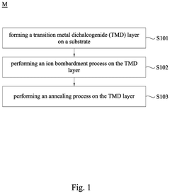
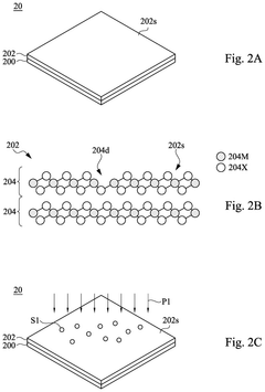
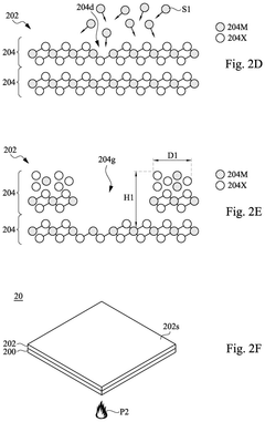
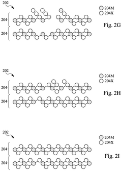
Semiconductor structure and manufacturing method thereof
PatentPendingUS20240332013A1
Innovation
- A two-step process involving ion bombardment to destroy bonds around intrinsic surface defects, followed by annealing at low temperatures to recrystallize the surface, effectively reducing defect density on TMD layers.
Method of depositing a transition metal dichalcogenide
PatentPendingUS20240124975A1
Innovation
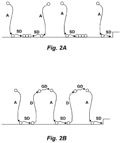
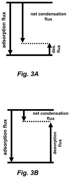
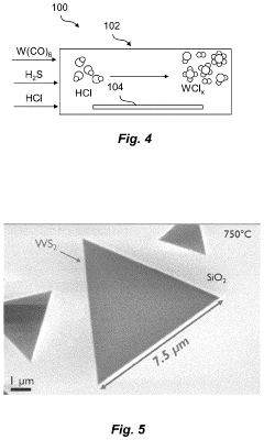
- Incorporating a gas-phase halogen-based reactant into the MOCVD process with transition metal and chalcogen precursors to enhance desorption rates and promote long-range diffusional transport, reducing nucleation density and enabling the growth of micrometer-scale monocrystalline layers by maintaining low supersaturation conditions.
Characterization Methods for TMD Defect Analysis
Accurate characterization of defects in CVD-grown TMD monolayers is essential for developing effective defect reduction strategies. Various analytical techniques provide complementary information about defect types, densities, and distributions, enabling researchers to optimize growth parameters systematically.
Optical microscopy serves as the initial characterization method, allowing rapid assessment of sample coverage and uniformity. While limited in resolution, it provides valuable information about large-scale defects and domain boundaries. Photoluminescence (PL) spectroscopy offers insights into the optical quality of TMD monolayers, with defect-rich areas typically showing reduced PL intensity and peak broadening, making it an effective non-destructive screening tool.
Raman spectroscopy provides critical information about crystal quality and strain distribution. The intensity ratios and peak positions of characteristic vibrational modes (E2g and A1g) correlate with defect densities, enabling quantitative assessment of sample quality across large areas. This technique is particularly valuable for identifying regions with varying defect concentrations before more detailed analysis.
Atomic Force Microscopy (AFM) delivers nanoscale topographical information, revealing surface defects, thickness variations, and grain boundaries. Advanced AFM modes such as Kelvin Probe Force Microscopy (KPFM) can map local electronic properties, providing insights into how defects affect charge distribution within the monolayer structure.
Scanning Tunneling Microscopy (STM) achieves atomic resolution imaging of TMD surfaces, enabling direct visualization of atomic defects including vacancies, substitutions, and adatoms. Combined with Scanning Tunneling Spectroscopy (STS), it provides detailed electronic structure information around defect sites, crucial for understanding how specific defects impact material properties.
Transmission Electron Microscopy (TEM), particularly aberration-corrected STEM, offers atomic-resolution imaging of TMD lattice structures. Techniques like High-Angle Annular Dark-Field (HAADF) imaging can distinguish between different atomic species, enabling precise identification of vacancy defects, substitutional impurities, and grain boundaries. In-situ TEM allows real-time observation of defect formation and evolution during thermal or electrical stimulation.
X-ray Photoelectron Spectroscopy (XPS) provides elemental composition and chemical state information, helping identify impurities and stoichiometric deviations. Secondary Ion Mass Spectrometry (SIMS) offers highly sensitive detection of trace impurities, while Time-of-Flight SIMS (ToF-SIMS) provides spatial mapping of defect distributions with high chemical specificity.
Integrating multiple characterization techniques is crucial for comprehensive defect analysis, as each method has inherent limitations. Advanced data analysis approaches, including machine learning algorithms, are increasingly employed to correlate multi-modal characterization data, enabling more accurate defect classification and quantification in CVD-grown TMD monolayers.
Scalability and Cost Considerations for Industrial Production
The transition from laboratory-scale production to industrial manufacturing of CVD-grown TMD monolayers presents significant economic and technical challenges. Current laboratory processes typically yield high-quality but small-area samples, with production costs ranging from $100-1000 per square centimeter, making commercial applications economically unfeasible at present scale.
Industrial scalability requires substantial modifications to existing CVD systems. Large-format reactors capable of uniform precursor distribution across 300mm wafers or larger substrates represent a critical infrastructure investment, typically costing between $2-5 million per production line. These systems must maintain precise temperature gradients and gas flow dynamics at larger scales to preserve the quality achieved in laboratory settings.
Precursor utilization efficiency emerges as a major cost driver, with current systems typically achieving only 5-15% utilization rates. Implementing precursor recycling systems and optimizing delivery methods could potentially reduce material costs by 60-70%, though such systems add complexity to the production line.
Throughput considerations significantly impact unit economics. Laboratory-scale processes often require 2-4 hours per growth cycle, whereas industrial viability demands cycle times under 30 minutes. Batch processing capabilities, where multiple substrates undergo simultaneous growth, offer a promising approach to improving throughput without sacrificing quality control.
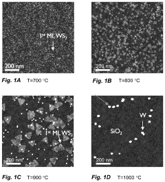
Energy consumption represents another substantial cost factor. The high temperatures (700-1000°C) required for conventional CVD growth translate to significant operational expenses. Alternative approaches such as plasma-enhanced CVD can reduce thermal budgets by 30-40%, though these methods often introduce new challenges in defect control.
Quality control and inspection costs increase with production scale. Automated optical inspection systems capable of detecting nanoscale defects across large areas represent a necessary investment of $500,000-1,000,000 per production line, but can significantly reduce downstream costs associated with defective materials.
Return on investment calculations suggest that achieving economically viable production requires defect densities below 10^10 cm^-2 while maintaining production costs under $10 per square centimeter. This target necessitates both technical innovations in growth processes and economies of scale in production infrastructure. Industry projections indicate that reaching these economic thresholds could enable mass adoption in electronics applications by 2026-2028, contingent upon continued progress in defect reduction strategies.
Industrial scalability requires substantial modifications to existing CVD systems. Large-format reactors capable of uniform precursor distribution across 300mm wafers or larger substrates represent a critical infrastructure investment, typically costing between $2-5 million per production line. These systems must maintain precise temperature gradients and gas flow dynamics at larger scales to preserve the quality achieved in laboratory settings.
Precursor utilization efficiency emerges as a major cost driver, with current systems typically achieving only 5-15% utilization rates. Implementing precursor recycling systems and optimizing delivery methods could potentially reduce material costs by 60-70%, though such systems add complexity to the production line.
Throughput considerations significantly impact unit economics. Laboratory-scale processes often require 2-4 hours per growth cycle, whereas industrial viability demands cycle times under 30 minutes. Batch processing capabilities, where multiple substrates undergo simultaneous growth, offer a promising approach to improving throughput without sacrificing quality control.
Energy consumption represents another substantial cost factor. The high temperatures (700-1000°C) required for conventional CVD growth translate to significant operational expenses. Alternative approaches such as plasma-enhanced CVD can reduce thermal budgets by 30-40%, though these methods often introduce new challenges in defect control.
Quality control and inspection costs increase with production scale. Automated optical inspection systems capable of detecting nanoscale defects across large areas represent a necessary investment of $500,000-1,000,000 per production line, but can significantly reduce downstream costs associated with defective materials.
Return on investment calculations suggest that achieving economically viable production requires defect densities below 10^10 cm^-2 while maintaining production costs under $10 per square centimeter. This target necessitates both technical innovations in growth processes and economies of scale in production infrastructure. Industry projections indicate that reaching these economic thresholds could enable mass adoption in electronics applications by 2026-2028, contingent upon continued progress in defect reduction strategies.
Unlock deeper insights with Patsnap Eureka Quick Research — get a full tech report to explore trends and direct your research. Try now!
Generate Your Research Report Instantly with AI Agent
Supercharge your innovation with Patsnap Eureka AI Agent Platform!