

Conformal Coating Methods for Complex PCB Geometries
SEP 17, 20259 MIN READ
Generate Your Research Report Instantly with AI Agent
PatSnap Eureka helps you evaluate technical feasibility & market potential.
Conformal Coating Evolution and Objectives
Conformal coating technology has evolved significantly since its inception in the 1960s, initially developed for military and aerospace applications where electronic components required protection against harsh environmental conditions. The progression from simple manual brushing techniques to sophisticated automated systems represents a fundamental shift in how protective coatings are applied to printed circuit boards (PCBs). Early conformal coating materials were primarily based on acrylic and epoxy formulations, offering basic protection but presenting challenges in terms of application uniformity and processing efficiency.
The 1980s and 1990s witnessed the emergence of silicone and polyurethane-based coatings, expanding the available material options and enhancing performance characteristics such as thermal stability, chemical resistance, and flexibility. This period also saw the introduction of selective coating technologies, allowing for more precise application to specific areas of PCBs while avoiding components that should remain uncoated.
Recent technological advancements have focused on addressing the increasing complexity of modern PCB designs, characterized by higher component densities, three-dimensional structures, and miniaturized features. The industry has responded with innovations in application methodologies, including robotic dispensing systems with multi-axis movement capabilities, advanced spray technologies with improved transfer efficiency, and plasma-enhanced deposition techniques that enable uniform coverage of intricate geometries.
The evolution of conformal coating has been driven by several key factors: the miniaturization trend in electronics, increasing reliability requirements for consumer electronics, the expansion of electronics into more demanding environments, and the growing emphasis on sustainability and environmental compliance. These drivers have pushed the development of water-based formulations, UV-curable systems, and nano-enhanced coatings that offer improved performance while reducing environmental impact.
The primary objectives of modern conformal coating technology for complex PCB geometries include achieving uniform coverage across varied topographies, ensuring protection of high-density interconnects, maintaining coating integrity in areas with significant height variations, and developing application methods that can adapt to increasingly complex board designs. Additionally, there is a focus on reducing processing time and material waste while maintaining or improving protection levels.
Looking forward, the technology trajectory points toward more intelligent coating systems incorporating real-time monitoring and adaptive application parameters, advanced materials with self-healing properties, and integration with broader manufacturing automation frameworks. The ultimate goal remains consistent: providing reliable environmental protection for electronic assemblies while adapting to the evolving challenges of modern electronics design and manufacturing.
Market Analysis for Complex PCB Protection Solutions
The global market for PCB protection solutions is experiencing robust growth, driven by increasing demand for reliable electronics in harsh environments. The conformal coating segment specifically is projected to reach $15.2 billion by 2026, growing at a CAGR of 5.8% from 2021. This growth is particularly pronounced in sectors requiring high reliability such as automotive electronics, aerospace, defense, medical devices, and industrial control systems.
Consumer electronics represents the largest market segment by volume, though automotive and aerospace applications command premium pricing due to stringent performance requirements. Regional analysis shows Asia-Pacific dominating manufacturing volume, with China accounting for approximately 60% of global PCB production. However, North America and Europe lead in high-value, specialized coating solutions for complex geometries.
Market demand is increasingly focused on solutions that can effectively protect increasingly miniaturized and densely populated PCBs with complex three-dimensional structures. Traditional coating methods struggle with consistent coverage around tight component spacing, under low-standoff components, and in high-aspect-ratio areas. This has created a specialized market segment specifically addressing complex geometry protection.
Customer requirements have evolved significantly, with emphasis on coatings that provide multiple protection functions simultaneously: moisture resistance, chemical protection, thermal stability, and mechanical shock absorption. Environmental regulations, particularly in Europe and North America, have accelerated the shift toward water-based and solvent-free coating solutions, creating market opportunities for innovative formulations.
The competitive landscape features both established chemical companies and specialized coating solution providers. Leading market players include Henkel, Dow Corning, Chase Corporation, and HB Fuller, who collectively control approximately 45% of the global market share. These companies are investing heavily in R&D to develop next-generation coating materials and application methods specifically designed for complex geometries.
Pricing trends indicate a premium market for selective coating solutions that can address complex geometries without masking, with customers willing to pay 30-40% more for precision application systems. The total cost of ownership, rather than just material costs, has become the primary decision factor for many OEMs, as they consider equipment investment, process integration, and long-term reliability benefits.
Market forecasts suggest specialized coating solutions for complex PCB geometries will grow at nearly twice the rate of traditional coating methods over the next five years, representing a significant opportunity for innovation and market differentiation.
Current Challenges in Coating Complex PCB Geometries
Despite significant advancements in conformal coating technologies, protecting complex PCB geometries presents persistent challenges for manufacturers. Modern PCBs feature increasingly dense component placement, fine-pitch components, and three-dimensional structures that create numerous coating obstacles. The miniaturization trend in electronics has resulted in boards with components spaced mere millimeters apart, creating capillary gaps where coating materials can accumulate and cause defects such as bridging and webbing.
High-profile components present particular difficulties as they create shadowing effects during spray application processes. These shadowed areas often receive insufficient coating coverage, leaving critical areas vulnerable to environmental factors. Conversely, recessed areas and tight spaces between components tend to experience pooling issues, where excess coating material accumulates and fails to properly cure, leading to potential reliability problems.
Edge coverage represents another significant challenge, as board edges often remain inadequately protected due to surface tension effects that cause coating materials to pull away from sharp edges. This phenomenon, known as edge-pull or edge-creep, creates vulnerability points for moisture ingress and corrosion initiation.
The increasing use of heat-sensitive components further complicates coating processes. Many modern components cannot withstand the elevated temperatures required for optimal curing of traditional coating materials. This thermal constraint limits material selection and processing parameters, potentially compromising coating performance.
Complex connector geometries present additional challenges, as masking these areas is labor-intensive and prone to human error. Inadequate masking can result in coating ingress into connector interfaces, causing electrical contact issues and potential system failures. The precision required for effective masking increases production time and costs significantly.
Multi-board assemblies and flexible PCBs introduce further complications due to their non-planar surfaces and varying material properties. Coating materials must maintain consistent coverage across different substrate materials while accommodating mechanical stress from flexing or vibration.
The industry also faces challenges with coating verification on complex geometries. Traditional inspection methods struggle to detect coating defects in shadowed or recessed areas, leading to potential quality escapes. Advanced inspection technologies like UV fluorescence and automated optical inspection systems help address these issues but add complexity and cost to the manufacturing process.
Environmental and regulatory pressures further constrain coating solutions, as manufacturers must balance performance requirements with increasingly stringent VOC emissions regulations and hazardous material restrictions. This regulatory landscape limits the chemical formulations available for addressing complex geometry challenges.
Contemporary Coating Techniques for Complex PCBs
01 Spray coating techniques for complex PCB geometries
Spray coating methods are effective for applying conformal coatings to PCBs with complex geometries. These techniques use specialized nozzles and spray patterns to ensure uniform coverage over irregular surfaces, components of varying heights, and hard-to-reach areas. Automated spray systems can be programmed to adjust spray parameters based on the specific geometry of the PCB, ensuring consistent coating thickness and protection even in challenging areas like under components or around tall elements.- Spray coating techniques for complex PCB geometries: Spray coating methods are widely used for applying conformal coatings to PCBs with complex geometries. These techniques involve atomizing the coating material and directing it onto the PCB surface, allowing for uniform coverage even in hard-to-reach areas. Automated spray systems can be programmed to adjust spray patterns, pressure, and distance based on the specific board geometry, ensuring consistent coating thickness and protection of sensitive components while navigating around tall components and tight spaces.
- Selective coating methods for high-density PCBs: Selective coating techniques allow for precise application of conformal coatings to specific areas of PCBs while keeping other areas, such as connectors and test points, coating-free. These methods are particularly valuable for high-density PCBs with numerous components. Techniques include masking, robotic dispensing, and programmable systems that can follow predefined patterns. This approach optimizes protection while maintaining electrical connectivity where needed and accommodating the varying heights and spacing of components on modern PCBs.
- Dip coating solutions for uniform coverage: Dip coating involves immersing the entire PCB assembly into a bath of conformal coating material and then withdrawing it at a controlled rate. This method provides excellent coverage for PCBs with uniform geometries and is effective for high-volume production. The withdrawal speed, viscosity of the coating material, and temperature control are critical parameters that determine coating thickness and uniformity. Special fixtures and orientation techniques can be employed to address drainage issues around complex geometries and prevent coating buildup in recessed areas.
- Vacuum coating for void-free protection of complex PCBs: Vacuum coating techniques apply conformal coatings in a vacuum chamber, ensuring penetration into tight spaces and under low-clearance components. This method is particularly effective for eliminating air pockets and voids in complex PCB geometries with densely packed components. The process involves placing the PCB in a vacuum chamber, introducing the coating material, and then releasing the vacuum to draw the coating into all spaces. This approach provides superior protection against moisture and contaminants in challenging environmental conditions.
- Automated robotic systems for precision coating application: Advanced robotic systems equipped with vision systems and precise motion control are used to apply conformal coatings to PCBs with complex geometries. These systems can adapt to varying board layouts and component heights by creating 3D maps of the PCB surface. Robotic applicators can adjust coating parameters in real-time based on the specific geometry encountered, ensuring consistent coverage while minimizing waste. These systems are particularly valuable for high-mix, low-volume production environments where PCB geometries frequently change.
02 Selective coating methods for high-precision applications
Selective coating techniques allow for precise application of conformal coatings to specific areas of PCBs while leaving other areas uncoated. These methods are particularly useful for complex geometries where certain components or connectors must remain coating-free. Techniques include automated robotic dispensing, masking systems, and programmable coating paths that follow the contours of the PCB. This approach minimizes waste, reduces processing time, and ensures critical areas receive appropriate protection while maintaining functionality of components that should not be coated.Expand Specific Solutions03 Vacuum coating processes for uniform coverage
Vacuum coating processes provide exceptional uniformity for conformal coating application on complex PCB geometries. By placing the PCB in a vacuum chamber, air is removed from small gaps and crevices before introducing the coating material, ensuring penetration into difficult areas. This method is particularly effective for high-density boards with tight spaces between components. The vacuum environment also accelerates curing and eliminates bubbles or voids in the coating, resulting in superior protection against environmental factors even in the most intricate board designs.Expand Specific Solutions04 Dip coating optimization for complex board structures
Dip coating methods can be optimized for complex PCB geometries through controlled immersion and withdrawal techniques. By carefully controlling the speed, angle, and duration of the dipping process, consistent coating thickness can be achieved even on boards with varying component heights and densities. Advanced dip coating systems incorporate tilt mechanisms and variable withdrawal rates to prevent coating pooling in recessed areas or insufficient coverage on elevated components. This method is particularly cost-effective for high-volume production while still addressing the challenges of irregular board topographies.Expand Specific Solutions05 Automated robotic coating systems for precision application
Automated robotic coating systems offer precise control over conformal coating application for complex PCB geometries. These systems use advanced vision technology and path planning algorithms to map the three-dimensional structure of the PCB and apply coating with exact thickness control. Robotic systems can navigate around tall components, apply different coating thicknesses to various board regions, and ensure consistent coverage of edges and corners. This approach minimizes human error, reduces material waste, and provides repeatable results even for the most challenging board designs.Expand Specific Solutions
Leading Manufacturers and Service Providers Analysis
The conformal coating market for complex PCB geometries is in a growth phase, driven by increasing demand for electronics protection in harsh environments. The market is expanding at a CAGR of approximately 7-8%, with significant technological advancements in coating materials and application methods. Leading players like Nordson Corp. and HzO, Inc. are developing specialized solutions for intricate PCB designs, while established companies such as DuPont de Nemours and H.K. Wentworth are focusing on environmentally friendly coating formulations. Samsung Electro-Mechanics and AT&S are integrating coating processes into advanced PCB manufacturing, creating comprehensive protection solutions. The technology is maturing with innovations in selective coating techniques, automated application systems, and UV-curable formulations that address the challenges of coating complex geometries while maintaining production efficiency.
Nordson Corp.
Technical Solution: Nordson has developed advanced selective conformal coating systems specifically designed for complex PCB geometries. Their technology combines precision automated dispensing with multi-axis robotic application systems that can navigate intricate board topographies. Their Film-Coater and FX Series utilize path optimization algorithms to ensure uniform coating thickness (25-250 microns) even around tall components and under low-standoff parts. The systems incorporate real-time viscosity control and laser height sensing to automatically adjust dispensing parameters based on board topography. Nordson's approach includes specialized nozzle designs that can coat at angles up to 60° to reach shadowed areas beneath components, and their systems achieve positioning accuracy of ±0.1mm while maintaining line speeds of up to 300mm/second for production efficiency.
Strengths: Superior precision in coating application with advanced robotics; excellent edge definition and minimal waste through selective application; comprehensive process control with integrated inspection systems. Weaknesses: Higher initial capital investment compared to conventional methods; requires more complex programming for each board design; maintenance demands for precision dispensing equipment.
HzO, Inc.
Technical Solution: HzO has pioneered Parylene-based thin-film conformal coating technology specifically engineered for complex PCB geometries. Their proprietary vacuum deposition process creates ultra-thin (typically 3-25 microns) uniform coatings that conform perfectly to intricate board features. The process involves vaporizing the Parylene dimer at approximately 150°C, then pyrolyzing it at 680°C to create a reactive monomer gas that polymerizes upon contact with the substrate at room temperature. This gas-phase deposition allows the coating to penetrate gaps as small as 0.01mm between components and under BGAs. HzO's technology achieves 100% coverage without bridging or pooling issues common in liquid applications, providing exceptional protection against moisture, chemicals, and dust while adding minimal weight to the assembly.
Strengths: Superior penetration capability for extremely complex geometries; pinhole-free coverage at very thin layers; excellent dielectric properties with minimal impact on RF/electrical performance. Weaknesses: Relatively slower process compared to spray methods; higher processing costs; requires specialized equipment and controlled environment; more difficult to rework coated boards.
Critical Patents and Innovations in Conformal Coating
Conformal coating system and method
PatentInactiveUS20110143021A1
Innovation
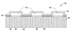
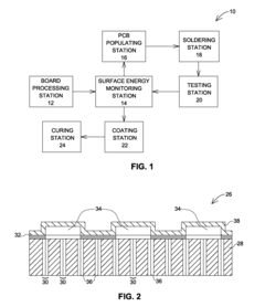
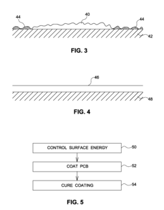
- A method and system that control and monitor the surface energy of printed circuit boards to ensure effective adhesion of a coating material without using saponifiers, using an ultraviolet cross-linkable polymer and maintaining surface energy above 50 dynes per square centimeter, thereby eliminating the need for saponifier cleaning and reducing cycle time.
Apparatus and method for conformal coating of integrated circuit packages
PatentActiveUS10356912B2
Innovation
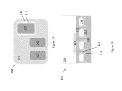
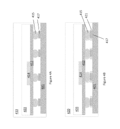
- A method that combines conformal coating and underfilling using parylene as a conformal coating layer that also functions as a second underfill layer, along with a thermally reworkable underfill layer, and includes a release agent layer to facilitate rework, reducing costs and time-to-market by streamlining the assembly process.
Environmental and Regulatory Compliance Factors
The regulatory landscape for conformal coating applications has become increasingly complex, with environmental considerations taking center stage in global manufacturing practices. RoHS (Restriction of Hazardous Substances) and REACH (Registration, Evaluation, Authorization and Restriction of Chemicals) regulations have significantly impacted material selection for conformal coatings, particularly limiting the use of certain solvents and chemicals traditionally employed in coating formulations. Manufacturers must now carefully evaluate coating materials to ensure compliance with these evolving standards while maintaining performance requirements for complex PCB geometries.
VOC (Volatile Organic Compound) emissions represent another critical regulatory concern, with stringent limitations imposed across different regions. Water-based and UV-curable coating systems have gained prominence as environmentally preferable alternatives to traditional solvent-based systems, offering reduced VOC emissions while providing adequate protection for intricate PCB designs. The transition to these greener alternatives has accelerated in regions with the most stringent environmental regulations, creating a tiered global market for conformal coating technologies.
Temperature and humidity requirements during application and curing processes must also align with workplace safety regulations. This is particularly challenging when coating complex PCB geometries that may require specialized application methods. Automated spray systems with advanced environmental controls have emerged as a solution to maintain regulatory compliance while ensuring coating quality and worker safety. These systems often incorporate filtration and recovery mechanisms to minimize environmental impact and meet local emission standards.
End-of-life considerations have become increasingly important in regulatory frameworks, with many jurisdictions implementing extended producer responsibility policies. Conformal coatings must now be evaluated not only for their protective properties but also for their impact on PCB recyclability and waste management. This has driven research into biodegradable coating options and materials that can be more easily separated during recycling processes, even when applied to complex geometries with multiple component types.
Industry-specific regulations add another layer of complexity, with medical, automotive, aerospace, and military applications each having unique requirements. For instance, medical device PCBs require biocompatible coatings that meet ISO 10993 standards, while automotive applications must satisfy IATF 16949 quality requirements. These specialized requirements often necessitate customized coating solutions that can conform to complex geometries while meeting sector-specific environmental and safety standards.
Global manufacturers must navigate this complex regulatory landscape while maintaining consistent quality across different markets. This has led to the development of universal coating solutions designed to meet the most stringent global standards, allowing companies to streamline their manufacturing processes while ensuring compliance across all operating regions. The ability to effectively apply these compliant coatings to complex PCB geometries remains a critical competitive advantage in the electronics manufacturing industry.
Quality Assurance and Testing Methodologies
Quality assurance and testing methodologies for conformal coating on complex PCB geometries require rigorous protocols to ensure complete protection and functionality. Inspection begins with visual examination under UV light, as most conformal coatings contain fluorescent additives that glow under ultraviolet illumination, revealing coating coverage, thickness variations, and potential defects such as bubbles, delamination, or uncoated areas. This non-destructive technique provides immediate feedback on coating uniformity across intricate board geometries.
Thickness measurement represents a critical quality parameter, typically assessed using micrometers, cross-sectioning techniques, or advanced optical measurement systems. For complex PCB geometries, confocal microscopy and 3D optical profiling have emerged as preferred methods, offering precise thickness mapping across irregular surfaces without contact damage. Industry standards generally specify coating thicknesses between 25-250 micrometers depending on the application environment and protection requirements.
Adhesion testing evaluates the coating's bond strength to the substrate, commonly performed through cross-hatch testing (per ASTM D3359) or pull-off adhesion testing. For complex geometries, specialized fixtures may be required to access difficult areas such as underneath components or within high-density interconnect regions. Environmental stress screening further validates coating performance through thermal cycling, humidity exposure, and salt spray testing.
Electrical insulation verification confirms the coating's primary protective function through insulation resistance testing and dielectric strength measurement. These tests are particularly important for high-frequency circuits and areas with fine-pitch components where coating thickness may vary. Specialized test fixtures with micro-probes enable targeted testing of critical areas on complex boards.
Automated optical inspection (AOI) systems equipped with machine learning algorithms have revolutionized quality control for conformal coatings. These systems can rapidly identify coating anomalies across complex geometries with greater consistency than manual inspection. Integration with production data allows for statistical process control and continuous improvement of coating parameters.
Accelerated aging tests simulate years of environmental exposure in compressed timeframes, subjecting coated boards to combined stresses including temperature cycling, humidity, UV exposure, and chemical exposure. These tests are essential for predicting long-term reliability in harsh operating environments such as automotive, aerospace, or industrial applications where complex PCB geometries are common.
Unlock deeper insights with PatSnap Eureka Quick Research — get a full tech report to explore trends and direct your research. Try now!
Generate Your Research Report Instantly with AI Agent
Supercharge your innovation with PatSnap Eureka AI Agent Platform!