

Cutting-edge encapsulation techniques for AMOLED displays.
JUL 17, 20259 MIN READ
Generate Your Research Report Instantly with AI Agent
PatSnap Eureka helps you evaluate technical feasibility & market potential.
AMOLED Encapsulation Evolution and Objectives
AMOLED (Active-Matrix Organic Light-Emitting Diode) displays have revolutionized the consumer electronics industry, offering superior image quality, energy efficiency, and design flexibility. The evolution of AMOLED technology has been closely tied to advancements in encapsulation techniques, which are crucial for protecting the sensitive organic materials from environmental factors such as moisture and oxygen.
The journey of AMOLED encapsulation began with rudimentary glass-to-glass sealing methods in the early 2000s. These initial approaches provided adequate protection but limited the potential for flexible displays. As the demand for thinner and more versatile devices grew, the industry shifted towards thin-film encapsulation (TFE) techniques, marking a significant milestone in AMOLED development.
The primary objective of cutting-edge encapsulation techniques for AMOLED displays is to achieve an optimal balance between protection and performance. This involves developing ultra-thin barrier layers that offer superior resistance to moisture and oxygen permeation while maintaining the display's flexibility and optical properties. Additionally, these techniques aim to extend the lifespan of AMOLED devices, enhance their durability, and enable new form factors such as foldable and rollable displays.
Current research focuses on multi-layer barrier films, often combining inorganic and organic materials to create a tortuous path for contaminants. Advanced atomic layer deposition (ALD) processes are being explored to deposit ultra-thin, highly uniform barrier layers with minimal defects. Hybrid encapsulation methods, which combine TFE with edge sealing techniques, are also under investigation to provide comprehensive protection against lateral ingress of contaminants.
The evolution of AMOLED encapsulation is driven by several key objectives. Firstly, there is a push towards reducing the overall thickness of the encapsulation layer to enable thinner and more flexible devices. Secondly, researchers are working on improving the barrier properties to achieve longer device lifetimes, particularly for applications in harsh environments. Thirdly, there is a focus on developing cost-effective encapsulation processes that can be scaled for mass production without compromising quality.
Looking ahead, the future of AMOLED encapsulation lies in the development of self-healing materials and smart barrier systems that can adapt to environmental changes. These innovations aim to create displays that are not only protected but also capable of repairing minor damage autonomously, further extending their lifespan and reliability.
Market Demand Analysis for Advanced AMOLED Displays
The market demand for advanced AMOLED displays has been experiencing significant growth, driven by the increasing adoption of smartphones, tablets, and wearable devices. As consumers seek higher quality visual experiences, AMOLED technology has become a preferred choice due to its superior color reproduction, contrast ratios, and energy efficiency compared to traditional LCD displays.
The smartphone segment remains the largest market for AMOLED displays, with high-end and mid-range devices increasingly incorporating this technology. Major smartphone manufacturers have been transitioning their flagship models to AMOLED screens, creating a ripple effect throughout the industry. This trend is expected to continue as production costs decrease and yield rates improve.
Wearable devices, particularly smartwatches, represent another rapidly growing market for AMOLED displays. The technology's ability to offer vibrant colors and deep blacks while consuming less power makes it ideal for small form factor devices with limited battery capacity. As the wearable market expands, the demand for AMOLED displays in this sector is projected to rise substantially.
The automotive industry is emerging as a promising new frontier for AMOLED technology. Advanced driver assistance systems (ADAS) and in-vehicle infotainment systems are increasingly adopting AMOLED displays for their superior visibility and aesthetic appeal. This trend is expected to accelerate as vehicle electrification and autonomous driving technologies progress.
Television manufacturers are also exploring AMOLED technology for high-end models, although the market penetration remains limited due to production challenges and costs associated with large-scale AMOLED panels. However, as manufacturing processes improve, the demand for AMOLED TVs is anticipated to grow, particularly in the premium segment.
The global AMOLED display market is projected to expand at a compound annual growth rate (CAGR) of over 20% in the coming years. This growth is fueled by technological advancements, increasing consumer preference for high-quality displays, and the expanding application areas for AMOLED technology.
Regionally, Asia-Pacific dominates the AMOLED display market, with South Korea and China leading in production and consumption. North America and Europe are also significant markets, driven by the high adoption rates of premium smartphones and growing interest in emerging technologies like foldable displays.
As the demand for AMOLED displays continues to rise, manufacturers are focusing on improving production efficiency and developing new form factors, such as flexible and foldable displays. These innovations are expected to open up new market opportunities and further drive the growth of the AMOLED display industry in the coming years.
Current Encapsulation Challenges and Limitations
Despite significant advancements in AMOLED display technology, encapsulation remains a critical challenge for manufacturers. The primary issue stems from the organic materials used in AMOLED displays being highly sensitive to moisture and oxygen. Even minute exposure can lead to rapid degradation of the organic layers, resulting in dark spots, reduced brightness, and shortened device lifespan.
Current encapsulation techniques, while effective to a degree, still struggle to provide the level of protection required for long-term stability. Thin-film encapsulation (TFE) is widely used but faces limitations in terms of achieving a perfect barrier against moisture and oxygen ingress. The multi-layer structure of TFE, typically alternating inorganic and organic layers, can develop defects during the deposition process, creating potential pathways for contaminants.
Another significant challenge is maintaining flexibility in encapsulation layers for foldable and flexible AMOLED displays. As devices become more bendable, the encapsulation must withstand repeated flexing without cracking or delaminating. This places additional stress on the barrier properties and adhesion of the encapsulation materials.
Temperature sensitivity presents another hurdle. The organic materials in AMOLEDs can degrade at high temperatures, limiting the processing options for encapsulation. This constraint makes it difficult to implement certain high-temperature deposition techniques that might otherwise provide superior barrier properties.
Scalability and cost-effectiveness of advanced encapsulation techniques pose significant challenges for mass production. While some cutting-edge methods show promise in laboratory settings, translating these into high-volume manufacturing processes without compromising quality or dramatically increasing costs remains problematic.
The industry also faces challenges in developing effective testing and quality control methods for encapsulation. Given the microscopic scale of potential defects and the long-term nature of degradation, it is difficult to accurately predict the lifespan of encapsulated displays or identify subtle flaws in the manufacturing process.
Lastly, the environmental impact of encapsulation materials and processes is becoming an increasing concern. As the electronics industry moves towards more sustainable practices, finding eco-friendly alternatives to current encapsulation materials and reducing the energy intensity of deposition processes are emerging as important challenges that need to be addressed.
State-of-the-Art Encapsulation Solutions
01 Thin film encapsulation for AMOLED displays
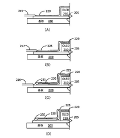
Thin film encapsulation is a crucial technology for AMOLED displays, providing protection against moisture and oxygen. This method involves depositing multiple layers of inorganic and organic materials to create a barrier that prevents degradation of the OLED elements. The process can be optimized for flexibility, transparency, and durability, enhancing the overall performance and lifespan of AMOLED displays.- Thin film encapsulation for AMOLED displays: Thin film encapsulation is a key technology for protecting AMOLED displays from moisture and oxygen. This method involves depositing multiple layers of inorganic and organic materials to create a barrier that prevents the degradation of the organic light-emitting materials. The process can include the use of atomic layer deposition (ALD) for inorganic layers and inkjet printing for organic layers, resulting in a thin, flexible, and effective encapsulation.
- Encapsulation with integrated touch sensors: Advanced AMOLED display encapsulation techniques incorporate touch sensors within the encapsulation layers. This integration reduces the overall thickness of the display module and improves touch sensitivity. The touch sensors can be made of transparent conductive materials and patterned to be nearly invisible, maintaining the display quality while adding touch functionality.
- Flexible AMOLED encapsulation: Encapsulation for flexible AMOLED displays requires materials and processes that can withstand bending and folding. This involves using flexible barrier films, stretchable adhesives, and specially designed layer structures that maintain their protective properties under mechanical stress. The encapsulation may also include stress-relieving layers to prevent damage to the OLED materials during flexing.
- Hybrid encapsulation techniques: Hybrid encapsulation combines different methods to achieve optimal protection for AMOLED displays. This can include a combination of thin film encapsulation with additional glass or metal lids, or the use of both inorganic and organic layers in specific arrangements. Hybrid approaches aim to leverage the strengths of various materials and deposition techniques to enhance the overall barrier properties and longevity of the display.
- Edge sealing for AMOLED encapsulation: Edge sealing is a critical aspect of AMOLED display encapsulation, preventing moisture and oxygen ingress from the sides of the display. Techniques include using specialized sealants, extending the encapsulation layers beyond the active area, or implementing additional barrier structures around the perimeter. Effective edge sealing contributes significantly to the overall lifetime and reliability of AMOLED displays.
02 Encapsulation with integrated touch sensors
Advanced encapsulation techniques for AMOLED displays incorporate integrated touch sensors within the encapsulation layers. This approach reduces the overall thickness of the display module while improving touch sensitivity and responsiveness. The integration of touch functionality into the encapsulation process can lead to more streamlined manufacturing and enhanced device performance.Expand Specific Solutions03 Flexible AMOLED encapsulation
Encapsulation methods for flexible AMOLED displays focus on maintaining barrier properties while allowing for bending and folding. These techniques often involve the use of specially formulated materials and deposition processes that can withstand mechanical stress. The goal is to create a flexible encapsulation layer that protects the OLED elements without compromising the display's ability to flex or fold.Expand Specific Solutions04 Encapsulation for improved display quality
Certain encapsulation techniques are designed to enhance the overall display quality of AMOLED screens. These methods focus on improving light extraction, color accuracy, and contrast ratios. By optimizing the encapsulation layers' optical properties, manufacturers can achieve better visual performance and energy efficiency in AMOLED displays.Expand Specific Solutions05 Advanced materials for AMOLED encapsulation
Research into new materials for AMOLED encapsulation aims to improve barrier properties, transparency, and durability. Novel inorganic compounds, hybrid organic-inorganic materials, and nanocomposites are being explored to create more effective encapsulation layers. These advanced materials can potentially lead to thinner, more robust, and longer-lasting AMOLED displays.Expand Specific Solutions
Key Players in AMOLED Encapsulation Industry
The AMOLED display encapsulation technology market is in a growth phase, driven by increasing demand for high-quality displays in smartphones, wearables, and other electronic devices. The market size is expanding rapidly, with major players like BOE Technology, TCL China Star Optoelectronics, and Everdisplay Optronics leading the charge. These companies are investing heavily in R&D to improve encapsulation techniques, aiming to enhance display performance and durability. The technology is maturing, with advancements in thin-film encapsulation and hybrid approaches. However, challenges remain in achieving perfect moisture and oxygen barriers, indicating room for further innovation and market growth.
BOE Technology Group Co., Ltd.
Technical Solution: BOE has developed advanced encapsulation techniques for AMOLED displays, including thin-film encapsulation (TFE) and hybrid encapsulation. Their TFE process utilizes alternating layers of inorganic and organic materials to create a barrier against moisture and oxygen. The inorganic layers, typically made of Al2O3 or SiNx, provide excellent barrier properties, while the organic layers offer flexibility and stress relief. BOE has also implemented atomic layer deposition (ALD) for ultra-thin, high-quality barrier films[1]. Additionally, they have explored the use of graphene as a barrier material, which offers exceptional impermeability to gases and moisture while maintaining flexibility[3]. BOE's hybrid encapsulation combines TFE with a glass cover, further enhancing the protection of sensitive OLED materials.
Strengths: Excellent barrier properties, flexibility, and stress relief. Potential for ultra-thin displays. Weaknesses: Complex manufacturing process, potential for defects in large-area displays.
Wuhan China Star Optoelectronics Semicon Display Tech Co.
Technical Solution: Wuhan China Star Optoelectronics has developed a multi-layer thin-film encapsulation (TFE) technology for AMOLED displays. Their approach utilizes a combination of inorganic and organic layers, with the inorganic layers typically composed of silicon nitride (SiNx) or aluminum oxide (Al2O3). The organic layers are made of specially formulated polymers that provide flexibility and act as a buffer between the rigid inorganic layers. They have implemented plasma-enhanced chemical vapor deposition (PECVD) for the inorganic layers and inkjet printing for the organic layers, allowing for precise control over layer thickness and uniformity[2]. The company has also explored the use of nanocomposite materials in their organic layers to further enhance barrier properties[4].
Strengths: Precise control over layer deposition, potential for high-throughput manufacturing. Weaknesses: Complexity in optimizing multi-layer structures, potential for increased production costs.
Breakthrough Encapsulation Patents and Research
Organic Light Emitting Diode Display Panel and Method for Encapsulating Same
PatentActiveUS20190363296A1
Innovation
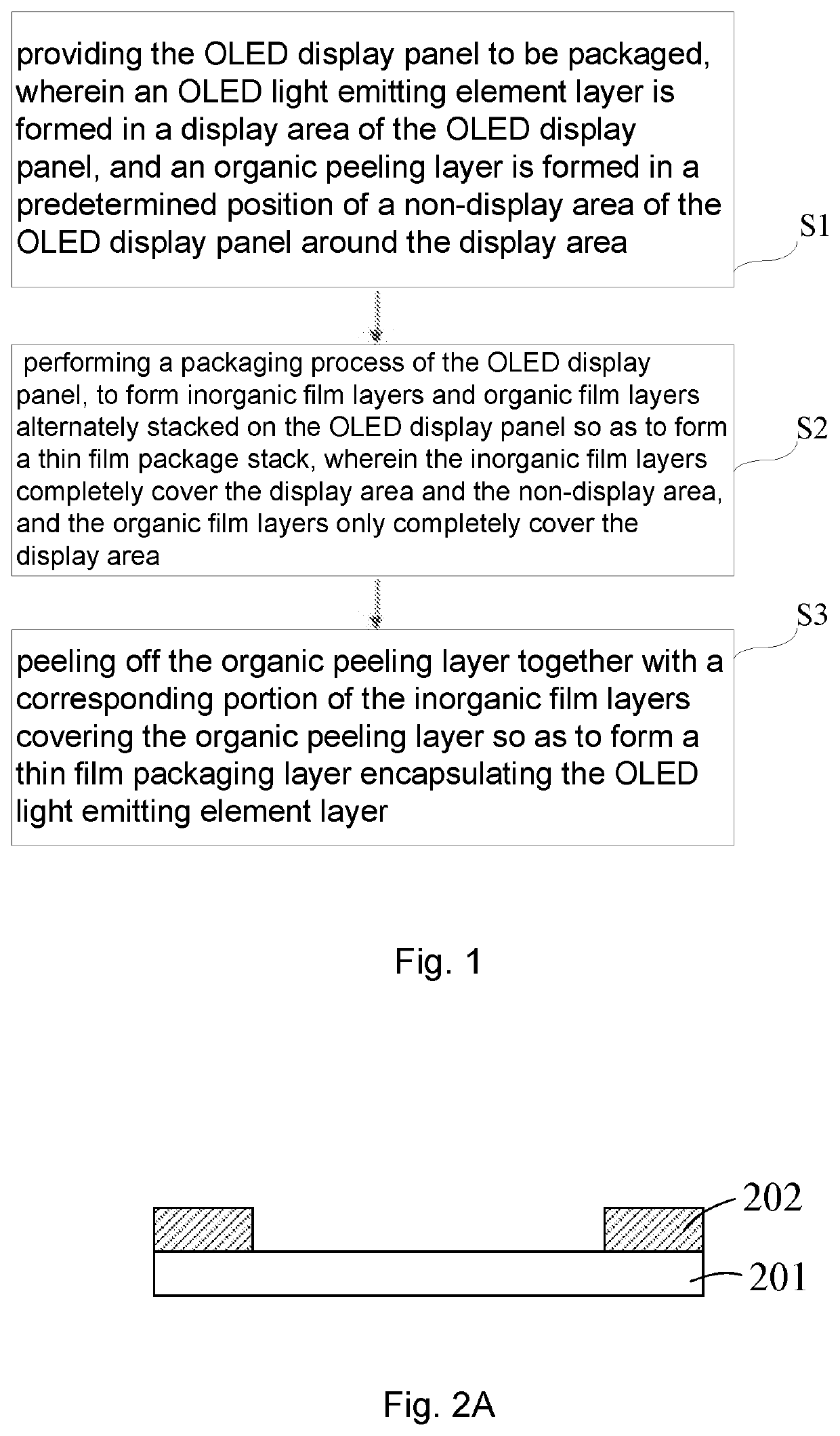
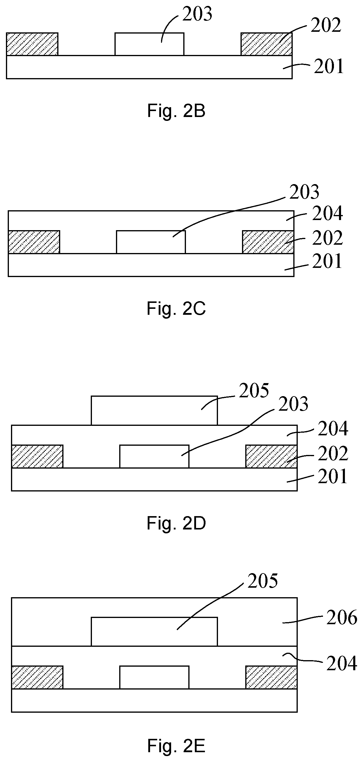
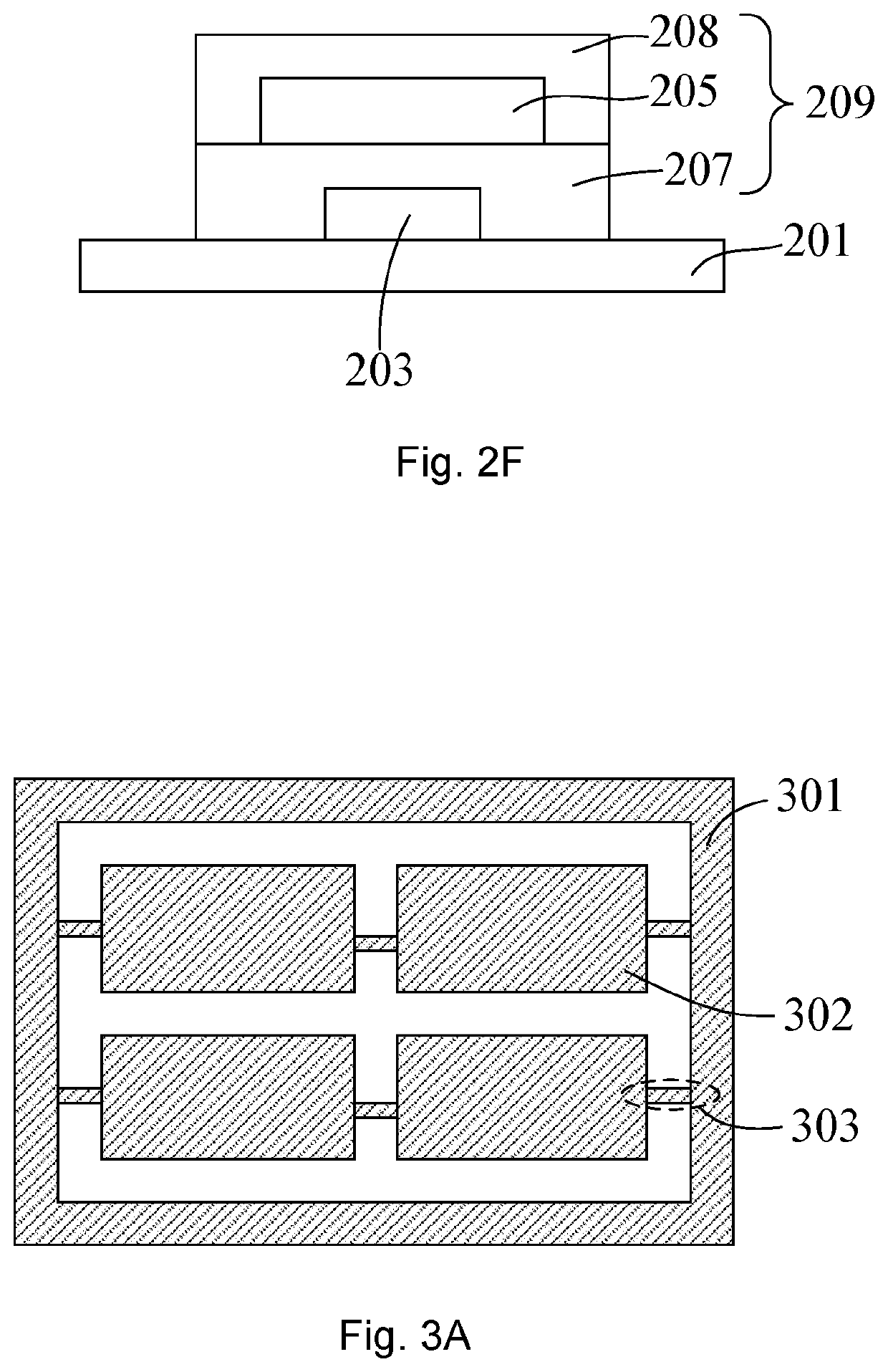
- A mask-free encapsulation method for OLED displays using a full-surface coating technique where inorganic and organic film layers are alternately stacked, with an organic peeling layer formed by thermal evaporation, allowing for the peeling off of encapsulation layers without the need for a mask, reducing production and maintenance costs.

Encapsulation method for organic light emitting diode
PatentInactiveJP2022145802A
Innovation
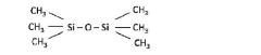
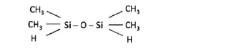
- A method involving the formation of inorganic and organic layers in a controlled process chamber, utilizing tunable buffer layers formed from vaporized organosilicon compounds like hexamethyldisiloxane or tetramethyldisiloxane, with precise mask alignment outside the chamber to ensure encapsulation integrity.
Environmental Impact of Encapsulation Materials
The environmental impact of encapsulation materials used in AMOLED displays is a critical consideration in the development of cutting-edge technologies. As the demand for AMOLED displays continues to grow, the industry must address the ecological footprint associated with their production and disposal.
Traditional encapsulation materials, such as glass and metal, have been widely used due to their excellent barrier properties. However, these materials often present challenges in terms of recycling and end-of-life management. Glass, while recyclable, requires significant energy input for processing, contributing to increased carbon emissions. Metal encapsulation, on the other hand, may introduce heavy metals into the environment if not properly handled during disposal.
Recent advancements in organic and hybrid encapsulation materials offer promising alternatives with potentially reduced environmental impact. Thin-film encapsulation (TFE) techniques, utilizing organic and inorganic layers, can significantly reduce the overall material usage while maintaining effective barrier properties. These materials are often lighter and more flexible, potentially reducing transportation-related emissions and energy consumption during manufacturing.
Biodegradable polymers are emerging as an eco-friendly option for encapsulation. These materials can break down naturally over time, reducing the long-term environmental burden. However, their barrier properties and longevity still need improvement to match the performance of traditional materials in AMOLED applications.
The production processes for advanced encapsulation materials also play a crucial role in their environmental impact. Atomic layer deposition (ALD) and plasma-enhanced chemical vapor deposition (PECVD) techniques used in TFE can be optimized for reduced energy consumption and minimal waste generation. However, these processes may involve the use of precursor chemicals that require careful handling and disposal to prevent environmental contamination.
Water-based and solvent-free encapsulation materials are gaining attention for their reduced volatile organic compound (VOC) emissions during manufacturing. These materials contribute to improved air quality in production facilities and surrounding areas, aligning with stricter environmental regulations worldwide.
The recyclability and reusability of encapsulation materials are becoming increasingly important. Research is ongoing to develop encapsulation systems that can be easily separated from other display components, facilitating more efficient recycling processes. This approach not only reduces waste but also conserves valuable resources used in AMOLED production.
As the industry moves towards more sustainable practices, life cycle assessments (LCAs) are being conducted to evaluate the environmental impact of different encapsulation materials and techniques. These assessments consider factors such as raw material extraction, manufacturing processes, energy consumption, and end-of-life scenarios to provide a comprehensive view of environmental performance.
Cost-Efficiency Analysis of Encapsulation Techniques
The cost-efficiency analysis of encapsulation techniques for AMOLED displays is a critical factor in determining the viability of new technologies in the market. Traditional encapsulation methods, such as glass-to-glass sealing, have been widely used but are often associated with high production costs and limitations in flexibility. As the demand for flexible and foldable displays increases, the industry is shifting towards more advanced thin-film encapsulation (TFE) techniques.
TFE methods, including atomic layer deposition (ALD) and plasma-enhanced chemical vapor deposition (PECVD), offer significant cost advantages in terms of material usage and process simplification. These techniques allow for the deposition of ultra-thin barrier layers, reducing material costs while maintaining excellent moisture and oxygen barrier properties. The initial investment in ALD and PECVD equipment can be substantial, but the long-term cost benefits often outweigh the upfront expenses.
One of the most promising cost-efficient encapsulation techniques is the hybrid approach, combining inorganic and organic layers. This method leverages the high barrier properties of inorganic materials with the flexibility and low-cost processing of organic materials. The alternating stack of these layers not only enhances the overall barrier performance but also allows for a reduction in the total thickness of the encapsulation structure, further driving down material costs.
The implementation of roll-to-roll (R2R) processing for encapsulation has shown potential for significant cost reductions in high-volume production. R2R techniques enable continuous, high-speed deposition of barrier layers, drastically reducing processing time and energy consumption. While the initial setup costs for R2R systems are high, the economies of scale achieved in mass production make it an attractive option for manufacturers looking to reduce per-unit costs.
Recent advancements in nanocomposite materials for encapsulation have also demonstrated promising cost-efficiency results. These materials offer enhanced barrier properties at lower thicknesses, reducing material usage and potentially simplifying the encapsulation process. The integration of nanoparticles or nanostructures into polymer matrices can provide a cost-effective alternative to multi-layer approaches while maintaining the required level of protection for AMOLED devices.
When considering the overall cost-efficiency of encapsulation techniques, it is crucial to factor in not only the direct material and processing costs but also the impact on device yield and long-term reliability. Advanced encapsulation methods that offer superior protection against moisture and oxygen ingress can significantly reduce failure rates and extend device lifetimes, thereby improving the overall cost-effectiveness of AMOLED production.
Unlock deeper insights with PatSnap Eureka Quick Research — get a full tech report to explore trends and direct your research. Try now!
Generate Your Research Report Instantly with AI Agent
Supercharge your innovation with PatSnap Eureka AI Agent Platform!