Discovering Advanced Properties of Polysilane Materials
JUL 11, 20259 MIN READ
Generate Your Research Report Instantly with AI Agent
Patsnap Eureka helps you evaluate technical feasibility & market potential.
Polysilane Evolution
Polysilane materials have undergone a remarkable evolution since their initial discovery in the mid-20th century. The journey of these silicon-based polymers began with the synthesis of poly(methylphenylsilane) by Burkhard in 1949, marking the inception of a new class of materials with unique optoelectronic properties.
In the 1960s and 1970s, researchers focused on developing various synthesis methods for polysilanes, including Wurtz-type coupling reactions and electrochemical reductive coupling. These advancements laid the foundation for exploring the structural diversity and potential applications of polysilanes.
The 1980s witnessed a surge in polysilane research, driven by the discovery of their semiconducting properties and photoconductivity. Scientists began to investigate the relationship between molecular structure and electronic properties, leading to the development of polysilanes with tailored characteristics for specific applications.
During the 1990s, the field expanded to include the exploration of hyperbranched and dendritic polysilanes, offering new possibilities for three-dimensional molecular architectures. This period also saw increased interest in the photophysical properties of polysilanes, particularly their potential use in photoresists and as precursors for silicon carbide ceramics.
The turn of the millennium brought about a shift towards nanoscale applications of polysilanes. Researchers began investigating their potential in nanoelectronics, photonics, and as building blocks for self-assembled nanostructures. This era also saw the development of novel polysilane-based hybrid materials, combining the unique properties of polysilanes with those of other organic or inorganic components.
In recent years, the focus has shifted towards discovering advanced properties of polysilanes, particularly in the realm of optoelectronics and energy applications. Scientists are exploring their potential in organic light-emitting diodes (OLEDs), photovoltaic devices, and as active materials in chemical sensors.
The evolution of polysilane materials has been marked by continuous improvements in synthesis techniques, characterization methods, and theoretical understanding of their electronic structure. From simple linear polymers to complex three-dimensional architectures, polysilanes have demonstrated remarkable versatility and potential for technological applications.
As research progresses, new frontiers are emerging in the field of polysilane materials. These include the development of stimuli-responsive polysilanes, exploration of their biological applications, and investigation of their role in next-generation quantum computing materials. The ongoing evolution of polysilanes continues to push the boundaries of materials science, promising exciting discoveries and innovations in the years to come.
Market Applications
Polysilane materials have emerged as promising candidates for various market applications due to their unique properties and versatile nature. The semiconductor industry has shown significant interest in these materials, particularly for their potential in optoelectronic devices. Polysilanes exhibit excellent photoconductivity and electroluminescence, making them suitable for applications in organic light-emitting diodes (OLEDs) and photovoltaic cells. Their ability to form stable thin films with high charge carrier mobility has attracted attention for use in transistors and other electronic components.
In the field of photoresists, polysilanes have demonstrated remarkable potential. Their high sensitivity to UV light and excellent resistance to plasma etching make them ideal for use in photolithography processes in the manufacturing of integrated circuits. This application has garnered interest from major semiconductor manufacturers looking to improve their production processes and achieve higher resolution in chip fabrication.
The aerospace and automotive industries have also recognized the value of polysilane materials. Their exceptional thermal stability and resistance to oxidation make them suitable for high-temperature applications, such as coatings for engine components and aerospace materials. Additionally, the lightweight nature of polysilanes contributes to fuel efficiency in transportation applications.
In the realm of energy storage, polysilanes show promise as electrode materials for next-generation batteries. Their unique electronic properties and ability to form stable structures with high surface area make them potential candidates for improving the performance and capacity of lithium-ion batteries and other energy storage devices.
The medical and biotechnology sectors are exploring polysilanes for drug delivery systems and biosensors. The biocompatibility of certain polysilane derivatives, combined with their ability to encapsulate and release drugs in a controlled manner, opens up possibilities for targeted drug delivery and improved therapeutic outcomes. Furthermore, the optical properties of polysilanes make them suitable for developing highly sensitive biosensors for medical diagnostics.
In the field of advanced materials, polysilanes are being investigated for their potential in creating self-healing polymers and smart materials. Their ability to undergo reversible bond breaking and reformation under specific conditions could lead to the development of materials with enhanced durability and longevity.
The growing interest in sustainable and environmentally friendly materials has also brought attention to polysilanes. Their potential for biodegradability and the ability to synthesize them from renewable resources align with the increasing demand for green technologies across various industries.
Technical Challenges
Polysilane materials have garnered significant attention in recent years due to their unique electronic and optical properties. However, the development and application of these materials face several technical challenges that need to be addressed for their full potential to be realized.
One of the primary challenges in polysilane research is the control of molecular weight and polydispersity. The properties of polysilanes are highly dependent on their chain length, and achieving precise control over these parameters remains difficult. Current synthetic methods often result in broad molecular weight distributions, which can lead to inconsistent material properties and performance.
Another significant hurdle is the stability of polysilanes under ambient conditions. Many polysilane materials are sensitive to oxygen and moisture, which can cause degradation and loss of their desirable properties. This instability limits their practical applications and poses challenges for long-term storage and use. Developing strategies to enhance the environmental stability of polysilanes without compromising their unique properties is crucial for their widespread adoption.
The processability of polysilanes presents another technical challenge. Many polysilanes have limited solubility in common solvents, making it difficult to process them into thin films or incorporate them into various devices. Improving the solubility and processability of polysilanes while maintaining their electronic and optical properties is essential for their integration into practical applications.
Furthermore, the optimization of charge transport properties in polysilane materials remains a significant challenge. While polysilanes exhibit interesting electronic properties, their charge carrier mobilities are often lower than those of traditional semiconducting materials. Enhancing the charge transport characteristics of polysilanes is crucial for their application in electronic devices and solar cells.
The development of efficient and scalable synthetic methods for polysilanes is another area that requires attention. Current synthetic routes often involve complex procedures or harsh reaction conditions, limiting the large-scale production of these materials. Developing more straightforward and environmentally friendly synthetic methods is essential for the commercial viability of polysilane-based technologies.
Additionally, the characterization of advanced properties in polysilane materials poses technical challenges. The unique electronic structure of polysilanes requires specialized analytical techniques to fully understand their behavior. Developing and refining characterization methods that can accurately probe the electronic and optical properties of polysilanes at various length scales is crucial for advancing the field.
Lastly, the integration of polysilanes into functional devices and systems presents its own set of challenges. Optimizing the interface between polysilanes and other materials, as well as developing appropriate device architectures that can fully exploit the properties of polysilanes, are areas that require further research and development.
Current Synthesis
01 Optical properties of polysilane materials
Polysilane materials exhibit unique optical properties, including high transparency and refractive index. These characteristics make them suitable for various optical applications, such as waveguides, optical fibers, and photonic devices. The optical properties can be tuned by modifying the molecular structure and composition of the polysilanes.- Optical properties of polysilane materials: Polysilane materials exhibit unique optical properties, including high transparency and refractive index. These properties make them suitable for various optical applications, such as waveguides, optical fibers, and photonic devices. The optical characteristics of polysilanes can be tuned by modifying their molecular structure and composition.
- Electrical and electronic properties of polysilanes: Polysilane materials possess interesting electrical and electronic properties, including semiconducting behavior and charge transport capabilities. These properties can be exploited in various electronic applications, such as organic field-effect transistors, photovoltaic devices, and sensors. The electronic properties of polysilanes can be tailored by controlling their molecular weight and side-chain substituents.
- Thermal and mechanical properties of polysilane materials: Polysilane materials exhibit good thermal stability and mechanical strength. These properties make them suitable for use in high-temperature applications and as structural materials. The thermal and mechanical properties of polysilanes can be enhanced by incorporating various functional groups or by forming composites with other materials.
- Chemical properties and reactivity of polysilanes: Polysilane materials possess unique chemical properties and reactivity, including their ability to undergo photochemical and thermal transformations. These properties make them useful in various applications, such as photoresists, precursors for ceramic materials, and chemical sensors. The chemical reactivity of polysilanes can be controlled by modifying their molecular structure and incorporating functional groups.
- Surface properties and functionalization of polysilane materials: Polysilane materials can be functionalized to modify their surface properties, such as wettability, adhesion, and biocompatibility. This allows for the development of polysilane-based materials with tailored surface characteristics for specific applications, including coatings, biomaterials, and nanocomposites. Various methods can be employed to functionalize polysilanes, such as chemical modification and plasma treatment.
02 Electrical and electronic properties of polysilanes
Polysilane materials possess interesting electrical and electronic properties, including semiconducting behavior and charge transport capabilities. These properties make them potential candidates for use in electronic devices, such as thin-film transistors, solar cells, and sensors. The electronic properties can be tailored by controlling the molecular weight and side-chain substituents of the polysilanes.Expand Specific Solutions03 Thermal and mechanical properties of polysilane materials
Polysilane materials exhibit good thermal stability and mechanical strength. These properties make them suitable for applications in high-temperature environments and as structural materials. The thermal and mechanical properties can be enhanced by incorporating various functional groups or by forming composite materials with other polymers or inorganic fillers.Expand Specific Solutions04 Chemical properties and reactivity of polysilanes
Polysilane materials possess unique chemical properties and reactivity, including the ability to undergo photochemical and thermal transformations. These properties make them useful in various applications, such as photoresists, precursors for ceramic materials, and chemical sensors. The chemical reactivity can be controlled by modifying the side-chain substituents and introducing functional groups along the polymer backbone.Expand Specific Solutions05 Surface properties and functionalization of polysilane materials
Polysilane materials can be functionalized to modify their surface properties, such as wettability, adhesion, and biocompatibility. This allows for the development of polysilane-based materials with tailored surface characteristics for specific applications, including coatings, biomaterials, and nanocomposites. Various techniques, such as plasma treatment and chemical modification, can be employed to achieve desired surface properties.Expand Specific Solutions
Industry Leaders
The field of advanced polysilane materials is in a nascent stage of development, characterized by ongoing research and emerging applications. The market size remains relatively small but is expected to grow as new properties and uses are discovered. Technological maturity is still evolving, with companies like JSR Corp., Henkel AG & Co. KGaA, and Covestro Deutschland AG leading in research and development. These firms are exploring potential applications in electronics, optics, and advanced coatings. Academic institutions such as South China Normal University and the Chinese Academy of Science Institute of Chemistry are also contributing significantly to the fundamental understanding of polysilane properties. As the technology progresses, collaboration between industry and academia will likely drive innovation and commercialization in this promising field.
Chinese Academy of Science Institute of Chemistry
Technical Solution: The Chinese Academy of Science Institute of Chemistry has made significant advancements in discovering advanced properties of polysilane materials. They have developed a novel synthesis method using catalytic dehydrogenative coupling of hydrosilanes, which allows for precise control over the molecular weight and structure of polysilanes[1]. This method enables the production of high-purity polysilanes with tailored properties. The institute has also explored the use of polysilanes as precursors for silicon carbide ceramics, demonstrating improved thermal stability and mechanical properties[2]. Additionally, they have investigated the photophysical properties of polysilanes, uncovering unique light-emitting characteristics that could be applied in optoelectronic devices[3].
Strengths: Strong expertise in polysilane synthesis and characterization, access to advanced research facilities. Weaknesses: Potential limitations in scaling up production for industrial applications, possible challenges in technology transfer to commercial partners.
Japan Science & Technology Agency
Technical Solution: The Japan Science & Technology Agency has been actively involved in advancing the field of polysilane materials. They have supported research into novel polysilane architectures, including the development of hyperbranched and dendritic polysilanes with unique optical and electronic properties[10]. The agency has also funded studies on the self-assembly behavior of polysilanes, leading to the discovery of new nanostructured materials with potential applications in photonics and sensing[11]. Furthermore, they have promoted research into the biocompatibility and biodegradability of polysilanes, opening up possibilities for their use in biomedical applications such as drug delivery systems and tissue engineering scaffolds[12].
Strengths: Broad research support network, ability to coordinate collaborative projects between academia and industry. Weaknesses: Limited direct control over research outcomes, potential challenges in translating research findings into commercial products.
Key Innovations
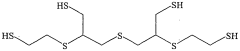
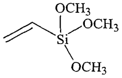
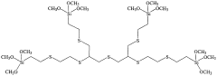
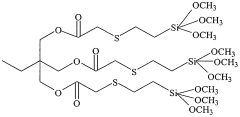
Sulfur modified silanes for the elaboration of high refractive index materials
PatentWO2009138853A1
Innovation
- A process involving the mixing of a polythiol and an alkenyl silane, followed by thiol-ene addition under UV radiation or heat, to produce polysulfide polysilanes with refractive indices ranging from 1.47 to 1.55, which can be further hydrolyzed to form high refractive index coatings and bulk materials with improved mechanical properties.
High-molecular polysilane and method for the production thereof for producing pre-ceramic molded bodies
PatentActiveUS20180200939A1
Innovation
- A method involving the reaction of silane monomers with aryl, alkyl, and alkenyl groups and alkali metals in an ether-containing solvent, such as dioxane, to produce high molecular weight polysilane with a stoichiometric silicon-to-carbon ratio, eliminating the need for sintering additives and annealing, thereby reducing porosity and enhancing mechanical stability.
Environmental Impact
The environmental impact of polysilane materials is a critical consideration in their development and application. These materials, known for their unique electronic and optical properties, have potential implications for both the natural environment and human health throughout their lifecycle.
Polysilanes are primarily composed of silicon and hydrogen, with the potential for various organic side groups. Their production process typically involves energy-intensive methods, such as the Wurtz coupling reaction or plasma-enhanced chemical vapor deposition. These processes can contribute to greenhouse gas emissions and energy consumption, highlighting the need for more sustainable manufacturing techniques.
During their use phase, polysilanes exhibit promising characteristics for environmental applications. Their photosensitivity and semiconducting properties make them suitable for solar cell technologies, potentially contributing to renewable energy solutions. Additionally, their use in photoresists for microelectronics manufacturing can lead to more efficient and miniaturized devices, indirectly reducing energy consumption in various electronic applications.
However, the disposal and degradation of polysilane materials present environmental challenges. While silicon-based materials are generally considered less toxic than many organic compounds, the long-term environmental fate of polysilanes and their degradation products is not fully understood. There are concerns about the potential release of nanoparticles or the formation of silica dust during weathering or incineration, which could have implications for air and water quality.
The recyclability of polysilane-based products is an area that requires further research and development. Current recycling technologies for silicon-based materials are primarily focused on crystalline silicon used in solar panels, and may not be directly applicable to polysilane materials. Developing efficient recycling methods for polysilanes could significantly reduce their environmental footprint and promote a circular economy approach.
Biodegradability is another aspect of environmental impact that needs consideration. While traditional plastics persist in the environment for extended periods, some research suggests that certain polysilane structures may be more susceptible to environmental degradation. This could potentially lead to the development of more environmentally friendly alternatives to conventional plastics in specific applications.
As research into advanced properties of polysilanes progresses, it is crucial to conduct comprehensive life cycle assessments to fully understand their environmental impact. This includes evaluating resource consumption, emissions, and potential toxicity at each stage of the material's life. Such assessments will guide the development of more sustainable polysilane materials and inform policy decisions regarding their use and disposal.
Characterization
Characterization of polysilane materials is crucial for understanding their advanced properties and potential applications. Various analytical techniques are employed to elucidate the structural, optical, and electronic characteristics of these materials.
Spectroscopic methods play a significant role in polysilane characterization. Nuclear Magnetic Resonance (NMR) spectroscopy provides valuable information about the chemical environment of silicon atoms and the degree of polymerization. Fourier Transform Infrared (FTIR) spectroscopy is used to identify functional groups and analyze the molecular structure of polysilanes. UV-Visible spectroscopy helps in studying the electronic transitions and optical properties of these materials.
X-ray diffraction (XRD) techniques are essential for investigating the crystalline structure of polysilanes. This method reveals information about the molecular packing, chain conformation, and degree of crystallinity. Additionally, small-angle X-ray scattering (SAXS) can provide insights into the nanoscale morphology and self-assembly behavior of polysilane materials.
Thermal analysis techniques, such as Differential Scanning Calorimetry (DSC) and Thermogravimetric Analysis (TGA), are employed to study the thermal properties and stability of polysilanes. These methods help in determining phase transitions, melting points, and decomposition temperatures, which are crucial for assessing the material's suitability for various applications.
Microscopy techniques, including Scanning Electron Microscopy (SEM) and Transmission Electron Microscopy (TEM), are used to examine the surface morphology and internal structure of polysilane materials at high resolution. Atomic Force Microscopy (AFM) provides detailed information about surface topography and mechanical properties at the nanoscale.
Electrochemical characterization methods, such as cyclic voltammetry and impedance spectroscopy, are employed to investigate the electronic properties and charge transport mechanisms in polysilanes. These techniques are particularly important for evaluating the potential of polysilanes in electronic and optoelectronic applications.
Advanced characterization techniques like X-ray Photoelectron Spectroscopy (XPS) and Secondary Ion Mass Spectrometry (SIMS) are used to analyze the surface composition and chemical state of polysilane materials. These methods provide valuable information about the elemental composition, bonding states, and depth profiles of the materials.
The combination of these characterization techniques allows researchers to gain comprehensive insights into the structure-property relationships of polysilane materials. This knowledge is essential for tailoring the properties of polysilanes and developing advanced materials with enhanced performance for various applications in electronics, photonics, and nanotechnology.
Unlock deeper insights with Patsnap Eureka Quick Research — get a full tech report to explore trends and direct your research. Try now!
Generate Your Research Report Instantly with AI Agent
Supercharge your innovation with Patsnap Eureka AI Agent Platform!