EMI Shielding Patent Landscape for Industrial Electronics Applications
SEP 25, 20259 MIN READ
Generate Your Research Report Instantly with AI Agent
Patsnap Eureka helps you evaluate technical feasibility & market potential.
EMI Shielding Evolution and Objectives
Electromagnetic Interference (EMI) shielding has evolved significantly since its inception in the early 20th century, initially emerging as a response to the growing complexity of electronic systems in military applications. The fundamental principle of EMI shielding—creating barriers that prevent electromagnetic radiation from interfering with sensitive electronic components—has remained consistent, though implementation methodologies have undergone substantial transformation.
The evolution of EMI shielding technology can be traced through several distinct phases. The 1950s-1970s marked the era of basic metallic enclosures, where aluminum and steel casings provided rudimentary protection. The 1980s-1990s witnessed the introduction of specialized conductive coatings and gaskets, enabling more targeted shielding solutions. The 2000s brought nanotechnology into the field, with carbon nanotubes and graphene emerging as revolutionary materials offering superior shielding effectiveness at reduced weights.
Current technological trends in EMI shielding for industrial electronics applications focus on addressing the challenges posed by miniaturization, increased operating frequencies, and the proliferation of wireless connectivity. The industry is witnessing a shift toward multi-functional shielding materials that not only block electromagnetic interference but also provide thermal management capabilities—a critical consideration as device densities increase.
The patent landscape reflects this evolution, with a noticeable surge in filings related to composite materials that combine traditional metallic shields with advanced polymers and nanomaterials. These innovations aim to deliver enhanced shielding effectiveness across broader frequency spectrums while maintaining mechanical flexibility and reducing overall weight.
The primary objectives of contemporary EMI shielding research and development center around several key areas: developing cost-effective solutions for mass production; creating environmentally sustainable shielding materials with reduced reliance on rare earth elements; improving shielding effectiveness at higher frequencies (particularly in the 5G spectrum and beyond); and designing solutions compatible with automated manufacturing processes.
For industrial electronics applications specifically, EMI shielding technologies must address the harsh operating environments often encountered in manufacturing settings, including exposure to chemicals, extreme temperatures, and mechanical stress. The goal is to develop robust shielding solutions that maintain their effectiveness throughout the extended lifecycle typical of industrial equipment, while simultaneously accommodating the increasing density of electronic components in modern industrial control systems.
Industrial Electronics EMI Protection Market Analysis
The industrial electronics EMI protection market is experiencing robust growth, driven by the increasing complexity of electronic systems and the growing demand for reliable operation in electromagnetically noisy environments. Current market valuations place the global EMI shielding market for industrial applications at approximately 6.5 billion USD in 2023, with projections indicating a compound annual growth rate of 5.8% through 2030. This growth trajectory is supported by the rapid expansion of industrial automation, Industry 4.0 initiatives, and the proliferation of sensitive electronic components in manufacturing environments.
Market segmentation reveals distinct categories within the industrial EMI protection sector. Conductive coatings represent the largest segment at 32% market share, followed by conductive polymers (24%), metal shielding (22%), EMI filters (15%), and other solutions (7%). Geographically, Asia-Pacific dominates the market with 42% share, particularly due to the high concentration of electronics manufacturing in China, Japan, and South Korea. North America and Europe follow with 28% and 23% respectively, with their markets primarily driven by advanced industrial automation and strict regulatory frameworks.
Key demand drivers include the increasing density of electronic components in industrial control systems, the growing adoption of wireless communication technologies in factory environments, and the rising concerns about electromagnetic compatibility in critical infrastructure. The automotive manufacturing sector represents the fastest-growing vertical, with a 7.2% annual growth rate in EMI protection implementation, followed closely by semiconductor fabrication facilities and energy production plants.
Customer requirements are evolving toward more integrated shielding solutions that offer multi-functional benefits beyond EMI protection, such as thermal management, environmental sealing, and mechanical protection. This trend is reflected in the 18% premium that customers are willing to pay for solutions that address multiple engineering challenges simultaneously.
Regulatory factors significantly influence market dynamics, with standards such as IEC 61000 series and regional certifications creating entry barriers but also ensuring market stability. The recent updates to electromagnetic compatibility regulations in the European Union and China have expanded the addressable market by approximately 12% as previously exempt devices now require EMI protection.
Emerging market opportunities include EMI protection for edge computing devices in industrial settings, shielding solutions for industrial IoT sensors, and specialized protection for high-power industrial equipment operating in harsh environments. These segments are projected to grow at 1.5-2 times the rate of the overall market in the next five years, representing significant opportunities for innovation and market expansion.
Current EMI Shielding Technologies and Barriers
The electromagnetic interference (EMI) shielding landscape for industrial electronics has evolved significantly over the past decade, with several established technologies dominating the market. Traditional metallic shields, particularly those made from aluminum, copper, and steel alloys, continue to be widely implemented due to their excellent conductivity and proven effectiveness. These solutions typically achieve shielding effectiveness of 60-120 dB across a broad frequency spectrum, making them suitable for many industrial applications.
Conductive coatings represent another major category, with silver, copper, and nickel-based formulations being particularly prevalent. These coatings can be applied through various methods including spraying, dipping, or vacuum metallization, offering flexibility in manufacturing processes. Recent advancements have improved adhesion properties and durability, addressing historical limitations of coating degradation over time.
Conductive polymers and composites have gained significant traction, combining the processability of plastics with moderate shielding capabilities. Carbon-filled composites, particularly those utilizing carbon nanotubes or graphene, have demonstrated promising results with shielding effectiveness reaching 30-70 dB while maintaining lighter weight profiles compared to metallic solutions.
Despite these technological advances, several barriers continue to challenge the EMI shielding field. Cost remains a primary concern, particularly for advanced materials like graphene-based composites or specialized metal alloys. The manufacturing complexity associated with these materials often requires substantial capital investment and specialized equipment, limiting widespread adoption across all industrial sectors.
Performance trade-offs present another significant challenge. Solutions that offer excellent shielding effectiveness often compromise on weight, flexibility, or thermal management capabilities. This creates particular difficulties in applications where multiple performance parameters must be optimized simultaneously, such as in compact industrial control systems or high-temperature environments.
Environmental considerations have emerged as an increasingly important barrier. Traditional shielding materials like beryllium copper alloys face growing regulatory scrutiny due to toxicity concerns. Additionally, the recyclability of composite materials remains problematic, creating end-of-life disposal challenges that conflict with sustainability initiatives being adopted across industrial sectors.
Integration complexity represents a persistent technical barrier, particularly as industrial electronics become more miniaturized and densely packed. Shield designs must accommodate complex geometries, multiple apertures for connectors, and heat dissipation requirements without compromising electromagnetic performance. This often necessitates customized solutions that increase development time and manufacturing costs.
Prevalent EMI Mitigation Approaches
01 Conductive materials for EMI shielding
Various conductive materials can be used for electromagnetic interference (EMI) shielding. These include metals, conductive polymers, and carbon-based materials that create a barrier to block electromagnetic radiation. The effectiveness of the shield depends on the material's conductivity, thickness, and configuration. These materials can be applied as coatings, films, or integrated into the structure of electronic devices to prevent electromagnetic interference.- Conductive materials for EMI shielding: Various conductive materials can be used to create effective EMI shields. These include metals like aluminum and copper, conductive polymers, and carbon-based materials such as graphene and carbon nanotubes. These materials work by reflecting or absorbing electromagnetic waves, preventing them from interfering with electronic components. The selection of material depends on factors such as shielding effectiveness requirements, weight constraints, and manufacturing considerations.
- Enclosure designs for electronic devices: Specialized enclosure designs can significantly improve EMI shielding in electronic devices. These designs include metal housings, conductive coatings, and compartmentalized structures that isolate sensitive components. Features such as gaskets at seams, conductive adhesives, and proper grounding techniques ensure continuous shielding across the entire enclosure. Advanced designs may incorporate multiple layers of different materials to address various frequencies of electromagnetic interference.
- Flexible and conformal shielding solutions: Flexible EMI shielding materials allow for protection of complex geometries and components with irregular shapes. These include conductive fabrics, elastomers, and thin films that can conform to various surfaces while maintaining shielding effectiveness. Such materials are particularly valuable in applications where rigid shields cannot be used, such as wearable electronics, flexible displays, and medical devices. These solutions often combine electrical conductivity with mechanical flexibility through specialized manufacturing techniques.
- Board-level shielding techniques: Board-level EMI shielding focuses on protecting individual components or sections of printed circuit boards. Techniques include shield cans, compartmentalization, and on-board Faraday cages. These solutions can be integrated during PCB design and manufacturing processes to isolate sensitive components from both external interference and cross-talk between board sections. Advanced board-level shielding may incorporate multiple layers and specialized vias to ensure comprehensive protection.
- Testing and verification methods: Specialized testing methods are essential to verify the effectiveness of EMI shielding solutions. These include near-field and far-field measurements, shielding effectiveness testing, and compliance verification for regulatory standards. Testing equipment such as spectrum analyzers, EMI receivers, and anechoic chambers help quantify shielding performance across different frequency ranges. These methods ensure that shielding solutions meet required specifications and regulatory requirements before product deployment.
02 EMI shielding in electronic enclosures and housings
Electronic enclosures and housings can be designed with integrated EMI shielding features to protect sensitive components from electromagnetic interference. These designs may include conductive gaskets, specialized coatings, or metal cages that surround electronic components. The housing structure itself can be manufactured using conductive materials or incorporate shielding layers to create a Faraday cage effect, effectively blocking electromagnetic radiation from entering or exiting the enclosure.Expand Specific Solutions03 Flexible and conformal EMI shielding solutions
Flexible and conformal EMI shielding solutions provide electromagnetic protection for irregularly shaped components or in applications where rigid shields are impractical. These include conductive fabrics, elastomers, adhesives, and sprays that can conform to complex geometries while maintaining shielding effectiveness. Such solutions are particularly valuable in portable electronics, wearable devices, and applications where weight and space constraints are significant considerations.Expand Specific Solutions04 EMI shielding connectors and interfaces
Specialized connectors and interfaces with EMI shielding capabilities are designed to maintain electromagnetic protection at points where cables and components connect to electronic devices. These connectors incorporate conductive elements, grounding mechanisms, and filtering components to prevent electromagnetic interference from entering or exiting through these potential weak points in the overall shielding system. Proper design of these interfaces is critical for maintaining the integrity of the EMI shield.Expand Specific Solutions05 EMI testing and measurement techniques
Various testing and measurement techniques are employed to evaluate the effectiveness of EMI shielding solutions. These include specialized equipment and methodologies to measure electromagnetic emissions, susceptibility, and shielding effectiveness across different frequency ranges. Testing procedures may involve anechoic chambers, network analyzers, and specialized probes to quantify how well a shield attenuates electromagnetic radiation. These measurements help ensure compliance with regulatory standards and verify that the shielding solution meets performance requirements.Expand Specific Solutions
Key EMI Shielding Solution Providers
The EMI shielding market for industrial electronics is in a growth phase, with increasing demand driven by the proliferation of electronic devices and stricter electromagnetic compatibility requirements. The market is characterized by a diverse competitive landscape featuring established electronics manufacturers and specialized shielding solution providers. Key players include Hon Hai Precision Industry (Foxconn) and Laird Technologies, which demonstrate advanced technical capabilities in shielding solutions. Major electronics corporations like Samsung, Apple, and Huawei are actively developing proprietary EMI shielding technologies to protect their industrial products. The technology is reaching maturity in traditional applications, while innovations in materials (particularly from companies like Nanotech Energy with graphene-based solutions) and miniaturization techniques are creating new growth opportunities in specialized industrial electronics segments.
Hon Hai Precision Industry Co., Ltd.
Technical Solution: Hon Hai (Foxconn) has developed extensive EMI shielding technologies for industrial electronics manufacturing. Their patented approach includes a dual-layer shielding system that combines vacuum-metallized plastic housings with secondary internal shields, providing cost-effective solutions for mass production[1]. Foxconn's proprietary conductive coating technology utilizes copper-filled epoxy resins that can be selectively applied to plastic enclosures, achieving 40-60 dB attenuation across 100 MHz to 6 GHz while maintaining design flexibility[3]. For industrial control systems, they've developed specialized EMI gaskets using metal-impregnated silicone that maintains conductivity even after multiple compression cycles in high-vibration environments[5]. Their recent innovations include automated robotic application systems for conductive adhesives that ensure consistent shield performance across high-volume manufacturing[7]. Foxconn has also patented modular shielding designs that allow for field-serviceable industrial electronics while maintaining EMI integrity, featuring interlocking shield segments with redundant contact points to ensure continuous electrical conductivity across seams[9].
Strengths: Exceptional manufacturing scalability; cost-effective solutions suitable for mass production; strong integration with existing manufacturing processes; extensive experience with diverse industrial applications. Weaknesses: Some solutions prioritize manufacturing efficiency over maximum shielding performance; certain proprietary techniques require specialized equipment; design flexibility may be limited compared to custom-engineered solutions; performance in extremely harsh environments may require additional protective measures.
Laird Technologies, Inc.
Technical Solution: Laird Technologies has developed advanced multi-layered EMI shielding solutions specifically designed for industrial electronics applications. Their technology incorporates specialized conductive elastomers and fabric-over-foam gaskets that provide both environmental sealing and EMI shielding in a single component[1]. The company's patented Board Level Shields (BLS) feature a two-piece design with a removable cover that allows for rework and repair while maintaining shielding integrity[3]. Laird's WaveThermal™ technology combines thermal management with EMI shielding through thermally conductive gap fillers that also provide electrical isolation[5]. Their Fingerstock gaskets utilize beryllium copper alloys with proprietary surface treatments to enhance conductivity and corrosion resistance, achieving up to 100 dB of shielding effectiveness across a broad frequency spectrum (10 MHz to 40 GHz)[7].
Strengths: Industry-leading shielding effectiveness across broad frequency ranges; integrated thermal management capabilities; customizable solutions for specific industrial applications; extensive material science expertise. Weaknesses: Higher cost compared to basic shielding solutions; some proprietary designs require specialized installation techniques; certain conductive materials may be subject to environmental degradation in harsh industrial environments.
Critical Patents in Industrial EMI Shielding
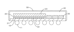
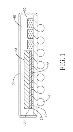
Electromagnetic interference shielding material, electromagnetic interference shielding device, method for making the electromagnetic interference shielding device, electromagnetic interference shielding package module and appliance
PatentInactiveUS20150085462A1
Innovation
- A mixture comprising 70 wt % to 98 wt % of dendritic copper filler, flaky copper filler, resin binder, and diluent is used to create an adjustable EMI shielding material that can be applied via screen printing or spraying, hardened at 120-160°C, providing effective shielding with adjustable thickness and low cost.
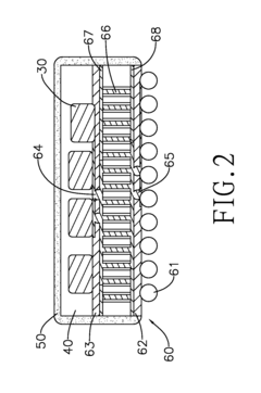
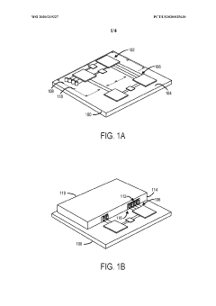
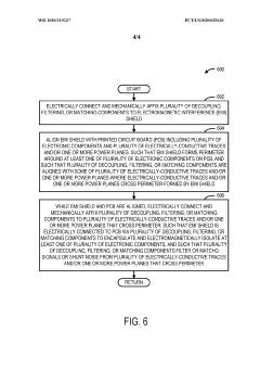
Electromagnetic interference shield with integrated decoupling
PatentWO2020219227A1
Innovation
- An EMI shield with integrated decoupling, filtering, or matching components that electrically connect between the shield and electrically-conductive traces or power planes on a PCB, allowing for effective shielding without a continuous ground plane, reducing PCB size and production costs, and providing flexible compatibility with various PCB layouts.
Regulatory Standards for EMI Compliance
The regulatory landscape for EMI compliance in industrial electronics applications is governed by a complex framework of international, regional, and national standards. The International Electrotechnical Commission (IEC) establishes the foundational standards through its CISPR (Comité International Spécial des Perturbations Radioélectriques) publications, particularly CISPR 11, which specifically addresses industrial, scientific, and medical equipment.
In the United States, the Federal Communications Commission (FCC) enforces Part 15 and Part 18 regulations, which set specific emission limits for electronic devices. These regulations categorize devices into Class A (industrial environments) and Class B (residential environments), with the latter having more stringent requirements due to proximity to sensitive consumer electronics.
The European Union implements the EMC Directive (2014/30/EU), which requires all electronic equipment sold within the EU to meet harmonized standards for both emissions and immunity. This directive is enforced through the CE marking system, requiring manufacturers to demonstrate compliance before market access is granted.
Military and aerospace applications follow more rigorous standards, such as MIL-STD-461G in the United States, which specifies detailed testing procedures and stricter emission limits due to the critical nature of these applications.
Recent regulatory trends show increasing harmonization efforts between different standards bodies, particularly between IEC and regional standards. However, significant differences remain in testing methodologies and compliance thresholds across jurisdictions, creating challenges for global manufacturers.
Emerging technologies like 5G and IoT industrial applications are driving regulatory evolution, with standards bodies working to address higher frequency ranges (up to 40 GHz) and more complex electromagnetic environments. The IEC 61000 series has been expanded to address these challenges, particularly focusing on immunity requirements for industrial control systems.
Compliance testing methodologies have also evolved, with greater emphasis on in-situ testing rather than laboratory-only evaluations. This shift recognizes the complexity of modern industrial environments and the limitations of traditional testing approaches in predicting real-world EMI issues.
Patent landscape analysis reveals significant innovation in compliance testing equipment and methodologies, with major test equipment manufacturers securing intellectual property around novel measurement techniques that align with evolving regulatory requirements.
Cost-Effectiveness Analysis of Shielding Solutions
The cost-effectiveness analysis of EMI shielding solutions for industrial electronics applications reveals significant variations across different technologies and implementation approaches. Traditional metallic shielding solutions, while offering excellent attenuation properties, often come with higher material costs and increased weight penalties that impact overall product economics. Sheet metal solutions typically range from $3-7 per square foot depending on material grade and thickness, with additional costs for secondary operations like forming and plating.
Conductive coatings present a more economical alternative at $1-4 per square foot, though their effectiveness diminishes in high-frequency applications above 1 GHz. The application process for these coatings requires specialized equipment, adding to initial capital investment but potentially reducing per-unit costs in high-volume production scenarios.
Emerging composite materials incorporating carbon nanotubes and graphene demonstrate promising cost-to-performance ratios, with current market prices trending downward from $15-20 per square foot in 2018 to $8-12 in 2023. This price reduction trajectory suggests these advanced materials may achieve cost parity with traditional solutions within 3-5 years while offering superior performance characteristics.
Implementation costs vary significantly based on design complexity and integration requirements. Retrofit shielding solutions typically incur 30-40% higher costs compared to designs where EMI considerations are incorporated from the outset. This highlights the economic advantage of early-stage EMI mitigation planning rather than addressing issues after design completion.
Patent analysis indicates a correlation between cost-effectiveness and application-specific optimization. Solutions designed for particular frequency ranges and environmental conditions demonstrate 15-25% better cost-performance ratios compared to general-purpose shielding approaches. This trend is particularly evident in patents filed since 2019, which increasingly focus on tailored solutions for specific industrial electronics applications.
Lifecycle cost analysis reveals that while initial implementation costs for advanced shielding solutions may be higher, reduced maintenance requirements and extended operational lifespans often result in favorable total cost of ownership. Particularly in harsh industrial environments, premium shielding solutions demonstrate 20-30% lower five-year ownership costs despite higher acquisition expenses.
Unlock deeper insights with Patsnap Eureka Quick Research — get a full tech report to explore trends and direct your research. Try now!
Generate Your Research Report Instantly with AI Agent
Supercharge your innovation with Patsnap Eureka AI Agent Platform!