Why EMI Shielding Improves Signal Integrity in High-Speed Electronics
SEP 25, 20259 MIN READ
Generate Your Research Report Instantly with AI Agent
Patsnap Eureka helps you evaluate technical feasibility & market potential.
EMI Shielding Evolution and Objectives
Electromagnetic Interference (EMI) shielding has evolved significantly since the early days of electronics, transitioning from simple metal enclosures to sophisticated multi-layered solutions designed to address increasingly complex interference challenges. The evolution of EMI shielding technology closely parallels the advancement of electronic devices, particularly as operating frequencies have increased and component sizes have decreased. In the 1950s and 1960s, EMI shielding primarily consisted of basic metal casings that provided rudimentary protection for low-frequency applications. By the 1970s and 1980s, as digital electronics became more prevalent, the need for more effective shielding solutions led to the development of specialized conductive coatings and gaskets.
The 1990s marked a significant turning point with the proliferation of wireless communication devices and higher frequency applications, necessitating more advanced shielding techniques. This period saw the introduction of selective shielding strategies and the integration of EMI considerations into early design phases rather than as afterthoughts. The 2000s brought nanotechnology into EMI shielding, with carbon nanotubes and graphene emerging as promising materials offering superior performance characteristics compared to traditional metal-based solutions.
Today's EMI shielding landscape is characterized by hybrid approaches that combine multiple materials and techniques to address the complex electromagnetic environments of modern high-speed electronics. The miniaturization trend in electronics has pushed shielding technology toward thinner, lighter solutions that maintain effectiveness while accommodating space constraints in densely packed devices. Additionally, environmental considerations have driven research into more sustainable shielding materials that reduce reliance on rare or toxic elements.
The primary objective of modern EMI shielding in high-speed electronics is to maintain signal integrity by preventing electromagnetic interference from disrupting critical operations. This involves not only blocking external interference sources but also containing emissions generated by the device itself. As data rates continue to increase, maintaining signal integrity becomes increasingly challenging, making effective EMI shielding a critical component of high-performance electronic systems.
Another key objective is compliance with increasingly stringent regulatory standards governing electromagnetic emissions and susceptibility. These regulations vary by region and application, creating a complex compliance landscape that manufacturers must navigate. The military and aerospace sectors typically have the most demanding requirements, while consumer electronics must balance performance with cost considerations.
Looking forward, the technical goals for EMI shielding include developing solutions that can effectively address the challenges posed by emerging technologies such as 5G, IoT devices, and autonomous vehicles. These applications operate at higher frequencies and in more crowded electromagnetic environments than previous generations of electronics, requiring innovative approaches to EMI management that can adapt to dynamic interference conditions while maintaining the performance and reliability expected of modern electronic systems.
Market Demand for Signal Integrity Solutions
The signal integrity solutions market is experiencing robust growth driven by the increasing complexity and speed of electronic systems across multiple industries. As data rates continue to climb beyond 10 Gbps in mainstream applications and reach 100+ Gbps in cutting-edge systems, maintaining signal quality has become a critical challenge for hardware designers and manufacturers.
Market research indicates that the global signal integrity solutions market, which encompasses EMI shielding products, is projected to grow at a compound annual growth rate of 12.5% through 2028. This growth is primarily fueled by the telecommunications sector's transition to 5G and eventually 6G networks, which require unprecedented levels of signal purity to function reliably at higher frequencies.
Consumer electronics represents another significant market driver, with smartphones, tablets, and wearable devices packing increasingly powerful processors into ever-smaller form factors. This miniaturization trend creates severe electromagnetic interference challenges that must be addressed to maintain product performance and meet regulatory requirements. The automotive industry's shift toward electric vehicles and advanced driver assistance systems has similarly intensified demand for effective EMI shielding solutions.
Data center infrastructure expansion continues unabated globally, with high-speed interconnects between servers requiring sophisticated signal integrity management. Cloud computing providers are particularly sensitive to signal degradation issues as they directly impact service quality and operational efficiency. This segment shows the highest willingness to invest in premium shielding solutions that can demonstrably improve system reliability.
Healthcare and aerospace/defense sectors represent smaller but premium market segments with stringent requirements for signal integrity. Medical devices must maintain perfect signal quality to ensure diagnostic accuracy and patient safety, while defense applications require solutions that can withstand extreme environmental conditions while maintaining secure communications.
Regional analysis reveals that Asia-Pacific dominates manufacturing capacity for EMI shielding components, while North America leads in research and development of advanced materials and techniques. European markets show particular sensitivity to environmental considerations, driving demand for halogen-free and recyclable shielding solutions.
Customer requirements are evolving beyond simple electromagnetic compatibility compliance toward comprehensive signal integrity management. End users increasingly demand solutions that address multiple aspects of signal quality simultaneously, including EMI suppression, impedance matching, and thermal management. This trend is pushing suppliers to develop integrated approaches rather than standalone shielding products.
Current EMI Shielding Technologies and Limitations
The electromagnetic interference (EMI) shielding landscape has evolved significantly over the past decade, with current technologies broadly categorized into metallic, conductive polymer-based, and composite solutions. Traditional metallic shields, including aluminum, copper, and steel enclosures, remain the industry standard due to their excellent conductivity and established manufacturing processes. These solutions typically achieve shielding effectiveness of 60-120 dB across a wide frequency range, making them suitable for many high-speed electronic applications.
Conductive polymer-based shields have gained traction as lightweight alternatives, incorporating materials such as polypyrrole, polyaniline, and PEDOT:PSS. These materials offer the advantage of flexibility and reduced weight compared to metallic solutions, though they generally provide lower shielding effectiveness (40-80 dB) and may degrade over time due to environmental factors.
Carbon-based composite shields, particularly those utilizing graphene, carbon nanotubes (CNTs), and carbon fiber, represent the cutting edge of current EMI shielding technology. These materials combine lightweight properties with shielding effectiveness approaching that of metals, particularly in the high-frequency ranges critical for modern high-speed electronics.
Despite these advancements, significant limitations persist across all current EMI shielding technologies. Cost remains a primary constraint, with high-performance solutions often requiring expensive materials or complex manufacturing processes. This creates a barrier to widespread implementation, particularly in consumer electronics where price sensitivity is high.
Manufacturing complexity presents another challenge, especially for intricate shield designs required in densely packed electronic systems. The miniaturization trend in electronics has outpaced advancements in shielding fabrication techniques, creating a technological gap that impacts signal integrity in high-speed applications.
Frequency-specific performance limitations also plague current solutions. Many shielding materials exhibit reduced effectiveness at certain frequency bands, creating vulnerabilities in broadband applications. This is particularly problematic as electronic devices increasingly operate across multiple frequency ranges simultaneously.
Heat management represents another critical limitation, as many effective shielding materials also trap heat within electronic components. This thermal constraint often forces design compromises that reduce shielding effectiveness to maintain acceptable operating temperatures, directly impacting signal integrity.
Weight and space considerations further restrict shielding options in portable and compact devices, where every gram and millimeter matters. The trade-off between shielding effectiveness and physical constraints often results in suboptimal protection against EMI, leading to degraded signal integrity in high-speed circuits.
Modern EMI Mitigation Techniques
01 Conductive enclosures and housings for EMI shielding
Conductive enclosures and housings can be used to shield electronic components from electromagnetic interference while maintaining signal integrity. These structures typically use metal or metallized materials to create a Faraday cage effect, blocking external EMI from affecting sensitive components inside. The design of these enclosures often includes features like gaskets, conductive coatings, and specialized apertures to maintain shielding effectiveness while allowing necessary connections and thermal management.- Conductive enclosures and housings for EMI shielding: Conductive enclosures and housings can be used to shield electronic components from electromagnetic interference while maintaining signal integrity. These structures typically use metal or metallized materials to create a Faraday cage effect that blocks external electromagnetic radiation from affecting sensitive components inside. The design of these enclosures often includes features like gaskets, conductive coatings, and specialized apertures to maintain shielding effectiveness while allowing for necessary connections and thermal management.
- Shielded cables and connectors for signal integrity: Specialized cables and connectors with EMI shielding properties are essential for maintaining signal integrity in high-speed data transmission. These components typically incorporate conductive shields, braided meshes, or foils that surround signal conductors to prevent electromagnetic interference. Advanced connector designs may include features like grounding fingers, conductive gaskets, and filtered contacts to minimize signal degradation while providing effective EMI protection at connection points.
- PCB-level EMI shielding techniques: Various printed circuit board design techniques can be employed to enhance EMI shielding and signal integrity. These include the use of ground planes, guard traces, via stitching, and controlled impedance routing. Advanced PCB-level shielding may also incorporate embedded shielding layers, compartmentalization of sensitive circuits, and specialized board materials with superior EMI absorption properties. These techniques help to isolate sensitive signal paths from interference sources while maintaining proper signal characteristics.
- Advanced materials for EMI shielding: Novel materials and composites are being developed specifically for EMI shielding applications that require minimal impact on signal integrity. These include conductive polymers, metal-filled composites, nanomaterials like graphene and carbon nanotubes, and specialized absorptive materials. These advanced materials can be applied as coatings, films, or structural components to provide effective EMI shielding while maintaining electrical performance and addressing challenges related to weight, thickness, and manufacturing complexity.
- Integrated circuit and component-level EMI shielding: EMI shielding can be implemented directly at the integrated circuit or component level to protect sensitive devices while preserving signal integrity. Techniques include on-chip shielding structures, conformal shielding coatings, embedded ground planes, and specialized packaging technologies. These approaches provide localized protection at the source of potential EMI issues, allowing for more efficient system design and improved overall performance by addressing interference problems at their origin.
02 Conductive materials and coatings for EMI suppression
Various conductive materials and coatings can be applied to electronic components and circuit boards to suppress EMI while preserving signal integrity. These include conductive polymers, metal-filled composites, carbon-based materials, and specialized coatings that can be selectively applied to create EMI barriers. These materials provide effective shielding while being lightweight, cost-effective, and compatible with modern manufacturing processes, allowing for protection of high-speed signals from interference.Expand Specific Solutions03 PCB design techniques for EMI shielding and signal integrity
Specific printed circuit board design techniques can significantly improve EMI shielding while maintaining signal integrity. These include proper layer stackup with dedicated ground planes, controlled impedance routing, signal trace shielding, and strategic component placement. Advanced PCB designs incorporate features like guard traces, via stitching, and specialized ground structures to contain electromagnetic emissions and protect sensitive signal paths from external interference.Expand Specific Solutions04 Connector and interface shielding solutions
Specialized connector and interface designs provide EMI shielding at critical junction points while maintaining signal integrity. These include shielded connectors with metal shells, filtered connectors with integrated EMI suppression components, and gasket-sealed interfaces. Advanced connector designs incorporate features like 360-degree shielding, impedance matching, and integrated filtering to prevent EMI leakage at cable entry points while preserving high-speed signal quality.Expand Specific Solutions05 Integrated circuit packaging and shielding techniques
Advanced integrated circuit packaging incorporates EMI shielding features to protect sensitive components while maintaining signal integrity. These include on-chip shielding structures, conformal shields, embedded ground planes, and specialized IC packages with integrated EMI protection. These techniques address EMI at the component level, providing protection for high-speed signals directly at their source and preventing interference between closely packed components in modern electronic devices.Expand Specific Solutions
Leading EMI Shielding Material Manufacturers
EMI shielding in high-speed electronics has evolved into a critical technology as the industry progresses from early adoption to mainstream implementation. The market is experiencing robust growth, projected to reach $9.2 billion by 2026, driven by increasing demand for signal integrity in compact, high-performance devices. Leading companies like Intel, Samsung Electronics, and IBM are advancing sophisticated shielding solutions, while specialized firms such as Laird Technologies and Nanotech Energy focus on innovative materials including graphene-based shields. The technology maturity varies across applications, with consumer electronics seeing widespread implementation while automotive and medical sectors are rapidly adopting advanced solutions. As data rates continue to increase, EMI shielding becomes increasingly essential for maintaining signal integrity in densely packed electronic environments.
Intel Corp.
Technical Solution: Intel has developed comprehensive EMI shielding solutions for high-speed processors and computing systems that focus on maintaining signal integrity across increasingly faster data rates. Their approach combines on-die, package-level, and system-level shielding strategies. At the package level, Intel employs embedded faraday cage designs with strategically placed ground planes and vias that create effective EMI barriers while minimizing signal path disruption. Their advanced substrate technologies incorporate specialized EMI-absorbing materials between critical signal layers, reducing crosstalk by up to 85% in high-density interconnects[5]. For server and data center applications, Intel has pioneered adaptive EMI shielding techniques that dynamically adjust shielding characteristics based on operating frequencies, optimizing both electromagnetic compatibility and thermal performance. Their latest solutions integrate specialized conductive polymers with traditional metallic shields, creating hybrid structures that effectively attenuate emissions across the 2-40GHz spectrum critical for modern computing and communications systems[6].
Strengths: Deeply integrated solutions that address EMI at multiple levels of the computing architecture; extensive research capabilities and intellectual property portfolio; solutions optimized for the highest performance computing environments. Weaknesses: Technologies often tied to Intel's specific processor architectures; premium solutions may carry significant cost implications; implementation complexity requires specialized design expertise.
Samsung Electronics Co., Ltd.
Technical Solution: Samsung Electronics has pioneered integrated EMI shielding solutions specifically designed for high-density semiconductor packages and mobile devices. Their technology employs conformal shielding methods where specialized conductive materials are directly applied to semiconductor packages through physical vapor deposition (PVD) or sputtering processes. This approach creates ultra-thin (2-8μm) metallic layers that provide effective EMI protection without significantly increasing device dimensions[2]. Samsung has also developed advanced package-level shielding techniques that incorporate EMI protection directly into their semiconductor manufacturing process, enabling system-in-package (SiP) designs with built-in EMI mitigation. Their solutions achieve shielding effectiveness of 30-40dB across frequencies from 800MHz to 6GHz, critical for 5G applications. Additionally, Samsung has implemented specialized grounding techniques and shield patterns that minimize signal degradation while maintaining high-frequency performance in their flagship mobile devices[4].
Strengths: Highly integrated solutions that minimize space requirements; manufacturing expertise that enables mass production of shielded components; comprehensive approach that addresses both device-level and system-level EMI issues. Weaknesses: Proprietary technologies may limit compatibility with third-party components; specialized manufacturing processes increase initial production costs; solutions optimized primarily for consumer electronics may require adaptation for industrial applications.
Key Patents in EMI Shielding Technology
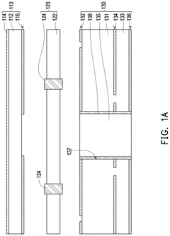
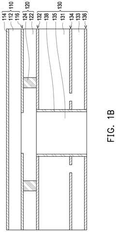
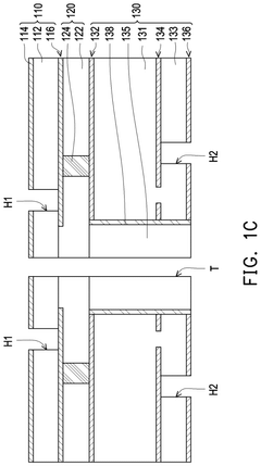
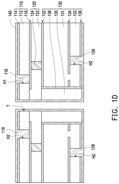
Manufacturing method of circuit board
PatentPendingUS20250056712A1
Innovation
- The circuit board design incorporates a conductive via structure that penetrates multiple substrates and dielectric layers, with conductive structures forming a ground path that surrounds the signal path, ensuring impedance matching and complete EMI shielding.
High-speed high-frequency signal transmission connector
PatentWO2024075995A1
Innovation
- A double shielding structure with surface contact between shield wall members effectively blocks EMI and reduces the connector's width direction size, utilizing a hermaphroditic connector design with specific shield wall configurations and pin arrangements for stable and reliable signal transmission.
Compliance Standards for EMI/EMC
Compliance with EMI/EMC standards is critical for electronic products to ensure they function reliably and do not interfere with other devices. The International Electrotechnical Commission (IEC) and the Federal Communications Commission (FCC) have established comprehensive frameworks that manufacturers must adhere to. These standards define acceptable limits for electromagnetic emissions and susceptibility across different frequency ranges and operating environments.
For high-speed electronics, the most relevant standards include CISPR 22/EN 55022 for information technology equipment, which categorizes devices into Class A (industrial) and Class B (residential) with corresponding emission limits. The IEC 61000 series addresses various aspects of electromagnetic compatibility, with IEC 61000-4 specifically focusing on testing and measurement techniques for immunity assessment.
Military and aerospace applications follow more stringent requirements outlined in MIL-STD-461, which provides detailed procedures for measuring both radiated and conducted emissions. This standard is particularly important for high-speed electronics operating in sensitive environments where signal integrity is paramount.
The automotive industry has developed specialized standards such as CISPR 25 and ISO 11452, addressing the unique challenges of vehicle electronics. These standards recognize that modern vehicles contain numerous high-speed electronic systems that must maintain signal integrity despite the electrically noisy environment.
Testing methodologies prescribed by these standards typically include measurements in anechoic chambers or on open area test sites. For signal integrity concerns, standards like IEC 62132 provide specific test methods for integrated circuits, while IEC 61967 addresses measurement of electromagnetic emissions.
Compliance certification processes generally involve pre-compliance testing during development, followed by formal testing at accredited laboratories. Documentation requirements include detailed test reports, technical construction files, and declarations of conformity. Many regions have adopted mutual recognition agreements to streamline the certification process across different markets.
Recent trends in compliance standards reflect the increasing speeds of electronic systems, with updates addressing higher frequency ranges and more complex signal integrity challenges. The emergence of 5G, IoT, and autonomous systems has prompted regulatory bodies to revise existing standards to accommodate these technologies while maintaining electromagnetic compatibility in increasingly crowded electromagnetic environments.
Cost-Benefit Analysis of EMI Solutions
When evaluating EMI shielding solutions for high-speed electronics, a comprehensive cost-benefit analysis is essential for making informed implementation decisions. The initial investment in EMI shielding materials and technologies varies significantly based on complexity and scale. Basic solutions such as metallic enclosures may cost between $5-20 per unit, while advanced composite materials or specialized coatings can escalate to $50-200 per component. For enterprise-level systems, comprehensive shielding implementations may represent 3-8% of total hardware costs.
Beyond material expenses, implementation costs include design modifications, testing procedures, and potential manufacturing process changes. These indirect costs often exceed the direct material expenses by 1.5 to 3 times, particularly when retrofitting existing designs rather than incorporating shielding during initial development phases.
The benefits side of the equation presents compelling economic advantages that frequently justify these investments. Signal integrity improvements directly translate to reduced error rates, with studies indicating a 30-60% decrease in bit error rates following proper EMI shielding implementation. This improvement significantly reduces costly system failures and data corruption incidents, which can average $5,000-25,000 per occurrence in enterprise environments.
Product reliability enhancements represent another substantial benefit. EMI-related failures account for approximately 15-30% of electronic system malfunctions in high-speed applications. Effective shielding can reduce these incidents by 40-70%, extending product lifespan by 20-40% and decreasing warranty claim expenses by 15-25% annually.
Regulatory compliance represents both a cost avoidance and market access benefit. FCC non-compliance penalties can reach $100,000 per violation, while EU regulations impose similar sanctions. Beyond direct penalties, non-compliant products face market restrictions and potential recall costs that can exceed millions of dollars for widespread deployments.
Time-to-market advantages also factor into the benefit calculation. Pre-emptive EMI shielding design reduces certification testing cycles by 30-50%, potentially accelerating market entry by 2-4 months. In competitive technology sectors, this acceleration can represent 10-15% of a product's total lifetime revenue through early market positioning.
The return on investment timeline typically shows EMI shielding solutions reaching break-even within 12-24 months for consumer electronics and 6-18 months for industrial or medical applications where reliability premiums are higher. Long-term ROI calculations frequently demonstrate 200-400% returns over a five-year product lifecycle when accounting for all direct and indirect benefits.
Unlock deeper insights with Patsnap Eureka Quick Research — get a full tech report to explore trends and direct your research. Try now!
Generate Your Research Report Instantly with AI Agent
Supercharge your innovation with Patsnap Eureka AI Agent Platform!