How EMI Shielding Layers Affect Device Miniaturization and Weight
SEP 25, 20259 MIN READ
Generate Your Research Report Instantly with AI Agent
PatSnap Eureka helps you evaluate technical feasibility & market potential.
EMI Shielding Evolution and Miniaturization Goals
Electromagnetic Interference (EMI) shielding has evolved significantly since its inception in the early 20th century. Initially, EMI shielding consisted of bulky metal enclosures that added substantial weight and volume to electronic devices. The primary focus was on functionality rather than form factor, with little consideration for device miniaturization. As electronics became more prevalent in consumer and industrial applications during the 1960s and 1970s, the need for more efficient shielding solutions emerged.
The 1980s marked a turning point with the introduction of conductive coatings and paints, offering weight reduction compared to traditional metal enclosures. The 1990s saw the development of metallized fabrics and conductive polymers, further advancing the field toward lighter solutions. By the early 2000s, thin-film deposition techniques enabled the creation of nanometer-scale shielding layers, dramatically reducing the weight and thickness of EMI protection.
Today's EMI shielding technologies represent a sophisticated balance between protection effectiveness and physical properties. Modern solutions include advanced composite materials, metalized plastics, conductive inks, and graphene-based shields that offer superior performance while minimizing dimensional impact. The integration of shielding directly into device components rather than as separate layers has become increasingly common, supporting the trend toward miniaturization.
The miniaturization goals for EMI shielding are driven by several factors in contemporary electronics design. Consumer demand for smaller, lighter devices with extended battery life creates pressure to reduce the footprint of all components, including shielding. The proliferation of wearable technology and IoT devices has intensified this need, as these applications are particularly sensitive to size and weight constraints.
Industry benchmarks now target EMI shielding solutions that add less than 5% to device weight and thickness while maintaining protection levels of 60-80 dB across relevant frequency ranges. For cutting-edge applications like medical implants and aerospace electronics, even more stringent goals exist, with shielding that adds less than 2% to device dimensions while withstanding harsh environmental conditions.
The technical trajectory points toward atomically thin shielding materials that can be conformally applied to complex geometries. Research into 2D materials like MXenes and functionalized graphene demonstrates potential for shielding effectiveness exceeding 70 dB with layers less than 1 micron thick. These developments align with the broader trend toward heterogeneous integration in electronics, where multiple functions are combined in minimal space.
Market Demand for Lightweight Shielded Devices
The global market for lightweight shielded electronic devices has experienced exponential growth over the past decade, driven primarily by consumer demand for smaller, lighter, and more portable technology. Market research indicates that consumers consistently rank device weight and size among their top three purchasing considerations, alongside performance and price. This trend is particularly evident in the smartphone sector, where manufacturers compete intensely to reduce device thickness while maintaining or improving EMI shielding capabilities.
In the medical device industry, demand for miniaturized shielded equipment has surged as healthcare providers seek portable diagnostic and monitoring tools that can be easily transported between patient rooms or used in home care settings. The wearable medical device market, which requires robust EMI shielding to ensure accurate readings and patient safety, is projected to grow at a compound annual rate exceeding 20% through 2028.
Aerospace and defense sectors represent another significant market driver, with requirements for lightweight shielded components that can withstand extreme conditions while minimizing payload weight. Each kilogram reduced in satellite components can translate to substantial launch cost savings, creating strong economic incentives for lightweight shielding solutions.
The automotive industry's transition toward electric and autonomous vehicles has dramatically increased the need for effective yet lightweight EMI shielding. Modern vehicles contain dozens of electronic control units and sensors that must operate reliably in close proximity, necessitating comprehensive shielding solutions that don't compromise fuel efficiency or battery range through added weight.
Consumer electronics manufacturers face particularly intense pressure to reduce device dimensions while maintaining electromagnetic compatibility. Market studies show that consumers perceive thinner devices as more premium and innovative, creating commercial incentives that directly influence product development priorities. This perception has established a clear market premium for devices that successfully integrate effective shielding without dimensional penalties.
Industrial IoT applications represent an emerging market segment with substantial growth potential for lightweight shielded devices. As factories and infrastructure become increasingly connected, the deployment of numerous sensors and communication modules creates both opportunities and challenges for EMI shielding technologies that must balance protection with weight and size constraints.
The telecommunications infrastructure market, particularly with the ongoing global 5G rollout, demands compact base station equipment that can be deployed in urban environments with minimal visual impact while maintaining signal integrity through effective shielding. This has created significant demand for innovative shielding approaches that minimize dimensional footprint without compromising performance.
Current EMI Shielding Technologies and Limitations
Electromagnetic Interference (EMI) shielding technologies have evolved significantly over the past decades, driven by the increasing demand for electronic device miniaturization and the growing complexity of electronic systems. Current EMI shielding solutions can be broadly categorized into metallic shields, conductive coatings, conductive polymers, and emerging nanomaterial-based solutions.
Traditional metallic shields, typically made from aluminum, copper, or steel alloys, remain the most widely used EMI shielding solution due to their excellent conductivity and shielding effectiveness. These shields operate by reflecting electromagnetic waves through their high electrical conductivity. However, they add considerable weight and volume to electronic devices, with shield thicknesses typically ranging from 0.1 to 0.5 mm, creating significant constraints for miniaturization efforts.
Conductive coatings represent a more space-efficient alternative, offering thinner shielding layers (10-50 μm) while maintaining acceptable shielding effectiveness. These coatings include metal-filled paints, vacuum metallization, and electroless plating. While they address some size constraints, they often suffer from durability issues, including susceptibility to scratching, oxidation, and delamination under thermal stress.
Conductive polymers have gained traction as lightweight alternatives, incorporating conductive fillers such as carbon black, metal particles, or conductive fibers within polymer matrices. These materials offer weight reductions of 40-60% compared to traditional metal shields but typically provide 10-20 dB less shielding effectiveness, requiring thicker layers to achieve comparable performance.
Emerging nanomaterial-based solutions, particularly those utilizing graphene, carbon nanotubes, and MXenes, represent the cutting edge of EMI shielding technology. These materials can achieve exceptional shielding effectiveness (>70 dB) at ultra-thin thicknesses (<100 μm). However, they face significant manufacturing challenges, including high production costs, scalability issues, and difficulties in uniform integration with existing manufacturing processes.
A critical limitation across all current technologies is the trade-off between shielding effectiveness and material thickness/weight. As devices continue to shrink, the proportional space and weight allocated to EMI shielding becomes increasingly significant, sometimes accounting for 5-15% of the total device volume in highly miniaturized electronics.
Another significant challenge is multi-functional integration. Modern device designs increasingly demand that shielding materials serve additional functions beyond EMI protection, such as heat dissipation, structural support, or environmental protection. Current technologies often require separate components for each function, further constraining miniaturization efforts.
The industry also faces regulatory challenges as emission standards become more stringent while device sizes decrease, creating an inherent technical contradiction that pushes existing shielding technologies to their physical limits.
Current Approaches to Balancing Shielding and Form Factor
01 Nanomaterial-based EMI shielding solutions
Advanced nanomaterials such as carbon nanotubes, graphene, and metal nanoparticles are being utilized to create ultra-thin EMI shielding layers. These materials offer excellent conductivity while maintaining minimal thickness and weight. The nanoscale dimensions of these materials allow for effective EMI shielding at significantly reduced thicknesses compared to traditional metal shields, making them ideal for miniaturized electronic devices where space and weight constraints are critical.- Nanomaterial-based EMI shielding solutions: Advanced nanomaterials such as carbon nanotubes, graphene, and metal nanoparticles are being incorporated into EMI shielding layers to achieve significant weight reduction while maintaining or improving shielding effectiveness. These materials offer exceptional electrical conductivity at extremely low thicknesses, allowing for the development of ultra-thin shielding layers that can be applied as coatings or integrated into composite structures. The high aspect ratio of these nanomaterials creates effective conductive networks that block electromagnetic radiation while adding minimal weight to the overall structure.
- Multilayer thin-film shielding structures: Multilayer thin-film structures combine different materials in precisely engineered layers to achieve optimal EMI shielding with minimal thickness and weight. These structures often alternate conductive and dielectric layers to create multiple reflection and absorption mechanisms for electromagnetic waves. Advanced deposition techniques such as sputtering, vapor deposition, and electroplating enable the creation of extremely thin yet effective shielding layers. This approach allows for customization of the shielding properties by adjusting the thickness, composition, and sequence of the layers.
- Conductive polymer composites for lightweight shielding: Conductive polymer composites incorporate conductive fillers such as metal particles, carbon fibers, or conductive polymers into a polymer matrix to create lightweight, flexible EMI shielding materials. These composites can be molded, extruded, or applied as coatings, offering significant design flexibility while reducing weight compared to traditional metal shields. The polymer matrix provides mechanical support and environmental protection, while the conductive fillers create pathways for electrical current that block electromagnetic radiation. These materials are particularly valuable for portable electronic devices where weight reduction is critical.
- Miniaturized EMI shielding for electronic packages: Specialized EMI shielding solutions for integrated circuits and electronic packages focus on miniaturization through techniques such as conformal shielding, embedded shielding layers, and compartmentalized shielding. These approaches integrate the shielding function directly into the electronic package or circuit board, eliminating the need for bulky external shields. Advanced manufacturing techniques such as laser direct structuring, selective plating, and 3D printing enable the creation of complex shielding geometries at the component level. This integration reduces the overall size and weight of electronic assemblies while providing effective EMI protection.
- Metamaterial and engineered structures for EMI shielding: Metamaterials and engineered structures with precisely designed geometrical patterns can manipulate electromagnetic waves to achieve superior shielding performance with minimal material usage. These structures use periodic arrangements of conductive elements to create frequency-selective surfaces or electromagnetic bandgaps that block specific frequency ranges. Advanced design techniques such as topology optimization and genetic algorithms help identify optimal geometries that maximize shielding effectiveness while minimizing weight and thickness. These engineered structures can achieve shielding performance that exceeds what would be possible with homogeneous materials of the same weight.
02 Multilayer composite shielding structures
Multilayer composite structures combine different materials with complementary properties to achieve optimal EMI shielding while minimizing thickness and weight. These structures typically consist of alternating conductive and dielectric layers, where each layer serves a specific function in the EMI shielding mechanism. By carefully engineering the thickness and composition of each layer, these composite structures can provide effective shielding across a broad frequency spectrum while maintaining minimal overall thickness and weight.Expand Specific Solutions03 Conductive polymer composites for lightweight shielding
Conductive polymer composites incorporate conductive fillers such as metal particles, carbon fibers, or graphene into polymer matrices to create lightweight EMI shielding materials. These composites offer significant weight advantages over traditional metal shields while maintaining adequate shielding effectiveness. The polymer matrix provides mechanical flexibility and reduced weight, while the conductive fillers create the necessary electrical pathways for EMI shielding. These materials can be formulated to achieve specific shielding requirements while optimizing for weight and thickness constraints.Expand Specific Solutions04 Miniaturized EMI shielding for semiconductor packages
Specialized EMI shielding solutions for semiconductor packages and integrated circuits focus on extreme miniaturization while maintaining effective shielding performance. These solutions include conformal shielding coatings, embedded shield layers within package substrates, and compartmentalized shielding structures. Advanced deposition techniques allow for the creation of ultra-thin metallic or composite shielding layers directly on semiconductor components, providing effective EMI protection without significantly increasing package dimensions or weight.Expand Specific Solutions05 Metamaterial and engineered structures for EMI shielding
Novel metamaterial structures and engineered electromagnetic surfaces are being developed to achieve superior EMI shielding with minimal thickness and weight. These structures utilize precisely designed patterns and geometries to manipulate electromagnetic waves rather than relying solely on material conductivity. By engineering specific resonant structures at the micro or nano scale, these solutions can selectively block electromagnetic radiation across targeted frequency bands while maintaining extremely thin profiles and lightweight construction, making them ideal for next-generation miniaturized electronic devices.Expand Specific Solutions
Key Industry Players in EMI Shielding Solutions
The EMI shielding market is currently in a growth phase, driven by increasing device miniaturization demands across consumer electronics and telecommunications. The global market is expanding at a CAGR of approximately 5.6%, with significant technological advancements focused on lightweight, thin shielding solutions. Leading players like Samsung Electronics, Intel, and Apple are investing in advanced composite materials that minimize weight while maintaining shielding effectiveness. Mid-tier manufacturers such as ROHM, ASE, and USI are developing specialized solutions for specific applications, while companies like TE Connectivity and 3M are focusing on innovative adhesives and flexible shielding materials. The industry is moving toward nano-materials and conductive polymers that offer superior EMI protection without compromising device form factors, with Taiwan Semiconductor and GLOBALFOUNDRIES integrating shielding directly into semiconductor packaging.
Samsung Electronics Co., Ltd.
Technical Solution: Samsung has developed advanced EMI shielding solutions specifically targeting device miniaturization challenges. Their proprietary conformal shielding technology applies ultra-thin metallic layers directly to semiconductor packages through physical vapor deposition (PVD) processes, achieving thicknesses as low as 5-10μm while maintaining effective shielding performance. This approach eliminates the need for traditional metal cans that typically add 0.2-0.5mm to device thickness. Samsung has also pioneered compartmentalized shielding techniques that create isolated chambers within devices to prevent cross-component interference, crucial for densely packed multi-function devices. Their latest innovation involves copper-filled through-mold vias that create a complete shielding cage around sensitive components, reducing overall footprint by up to 30% compared to conventional solutions while maintaining >60dB shielding effectiveness across key frequency bands.
Strengths: Achieves significant space savings with minimal impact on device weight; enables higher component density; maintains excellent shielding performance despite reduced material usage. Weaknesses: Requires specialized manufacturing equipment; higher initial production costs; potential thermal management challenges in ultra-compact designs due to heat concentration.
Intel Corp.
Technical Solution: Intel has developed sophisticated EMI shielding solutions specifically addressing the challenges of device miniaturization in high-performance computing applications. Their approach centers on embedded shielding technology that integrates EMI protection directly into the substrate and package design rather than adding it as a separate component. Intel's advanced package-level shielding employs copper-filled through-silicon vias (TSVs) and redistribution layers to create electromagnetic barriers around sensitive circuits, achieving shielding effectiveness of 40-70dB while adding minimal thickness (typically <50μm). For their latest mobile processors, Intel has implemented selective conformal shielding that targets only noise-critical areas, reducing shield weight by up to 60% compared to full-coverage approaches. Their research has demonstrated that optimized shield geometries with precisely engineered apertures can maintain effective shielding while using significantly less material. Intel has also pioneered the use of carbon nanotube-infused polymers as lightweight alternatives to traditional metal shields, achieving comparable performance at 30-40% lower weight in certain applications.
Strengths: Highly integrated approach minimizes impact on device dimensions; selective shielding optimizes weight distribution; compatible with advanced packaging technologies like chiplets. Weaknesses: Complex implementation requiring sophisticated design tools; potentially higher manufacturing costs; performance trade-offs in extremely space-constrained designs.
Critical Patents in Thin-Film EMI Shielding Technologies
Conforming, electro-magnetic interference reducing cover for circuit components
PatentInactiveUS7633015B2
Innovation
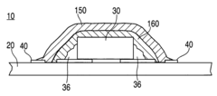
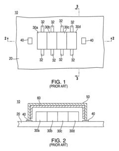
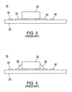
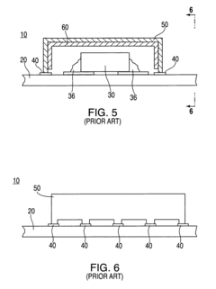
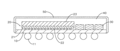
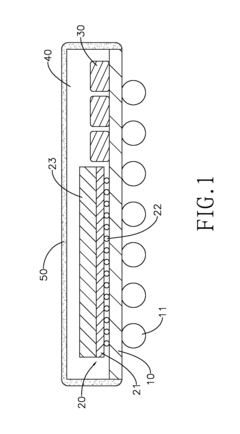
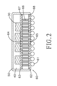
- Applying a conforming layer of electrical insulation that follows the shape of the electronic component, followed by a conforming layer of EMI shielding, which adheres and contacts the component surfaces, allowing for a more compact design by matching the shielding dimensions to the underlying circuitry.
Electromagnetic interference shielding material, electromagnetic interference shielding device, method for making the electromagnetic interference shielding device, electromagnetic interference shielding package module and appliance
PatentInactiveUS20150085462A1
Innovation
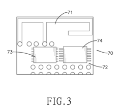
- A mixture comprising 70 wt % to 98 wt % of dendritic copper filler, flaky copper filler, resin binder, and diluent is used to create an adjustable EMI shielding material that can be applied via screen printing or spraying, hardened at 120-160°C, providing effective shielding with adjustable thickness and low cost.
Thermal Management Considerations in Compact Shielded Designs
The integration of EMI shielding layers in compact electronic devices creates significant thermal management challenges that must be addressed to maintain optimal performance. EMI shields, particularly those made of metals like aluminum or copper, can act as heat traps by restricting airflow and creating thermal barriers within the device. This phenomenon becomes increasingly problematic as device dimensions shrink, leading to potential hotspots and thermal runaway conditions.
Effective thermal management in shielded compact designs requires a multi-faceted approach. Heat dissipation pathways must be carefully engineered to work around or through shielding layers. Thermal vias, specialized heat-conducting channels that penetrate shield layers, have emerged as a critical solution for vertical heat transfer in multilayer PCB designs. These pathways allow heat to escape from sensitive components while maintaining electromagnetic containment.
Material selection plays a pivotal role in balancing thermal and EMI requirements. Thermally conductive EMI materials, such as graphene-enhanced composites and metal-filled polymers, offer dual functionality by simultaneously providing shielding and heat dissipation. These advanced materials typically exhibit thermal conductivity values between 1-20 W/mK while maintaining shielding effectiveness above 60dB across key frequency ranges.
The physical arrangement of components relative to shielding layers demands careful consideration in thermal design. Creating thermal zones within the device architecture allows for more efficient heat management, with high-heat-generating components strategically positioned to minimize thermal interference from shielding elements. This zoning approach must account for both steady-state and transient thermal conditions that occur during various operational modes.
Computational fluid dynamics (CFD) and thermal simulation tools have become essential for predicting how EMI shields affect thermal profiles in miniaturized devices. These simulations enable engineers to identify potential thermal bottlenecks before physical prototyping, significantly reducing development cycles. Recent advances in simulation technology now allow for concurrent electromagnetic and thermal modeling, providing a more comprehensive understanding of the shield-thermal interaction.
Innovative cooling solutions specifically designed for shielded compact devices continue to evolve. These include phase-change materials integrated within shield structures, micro-channel cooling systems that work in conjunction with shield layers, and advanced thermal interface materials that maximize heat transfer across shield boundaries while maintaining EMI protection integrity.
Environmental Impact of Advanced Shielding Materials
The environmental impact of advanced EMI shielding materials represents a critical consideration in the ongoing pursuit of device miniaturization and weight reduction. Traditional shielding materials such as copper, aluminum, and nickel-based alloys have significant environmental footprints throughout their lifecycle, from resource extraction to disposal. Mining operations for these metals contribute to habitat destruction, water pollution, and energy-intensive processing that generates substantial carbon emissions.
Advanced composite shielding materials, while offering superior performance-to-weight ratios, present their own environmental challenges. Carbon-based materials like graphene and carbon nanotubes require energy-intensive manufacturing processes that can offset their in-use environmental benefits. The production of conductive polymers often involves hazardous chemicals and solvents that pose risks to ecosystems if improperly managed.
Nanomaterial-based shields raise particular concerns regarding end-of-life management. Their novel properties that make them effective for EMI shielding also create uncertainties about their environmental fate and potential toxicity when released into ecosystems. The small particle size of nanomaterials increases their bioavailability and potential for bioaccumulation in organisms, with largely unknown long-term consequences.
The miniaturization trend enabled by advanced shielding materials creates a paradoxical environmental situation. While smaller devices generally require fewer raw materials and consume less energy during operation, they often become more difficult to repair and recycle. The complex integration of shielding layers with other components can make material separation challenging, potentially reducing recycling rates and increasing electronic waste.
Life cycle assessments of next-generation shielding materials reveal important trade-offs. Materials that enable significant weight reduction may deliver substantial environmental benefits during the use phase through improved energy efficiency and extended battery life. However, these benefits must be weighed against potentially higher environmental impacts during production and end-of-life phases.
Regulatory frameworks worldwide are increasingly addressing these concerns through extended producer responsibility programs and restrictions on hazardous substances. The electronics industry is responding with green design initiatives that consider environmental impacts throughout the product lifecycle, including the development of bio-based and biodegradable shielding materials that maintain performance while reducing environmental footprint.
Unlock deeper insights with PatSnap Eureka Quick Research — get a full tech report to explore trends and direct your research. Try now!
Generate Your Research Report Instantly with AI Agent
Supercharge your innovation with PatSnap Eureka AI Agent Platform!
