

Why EMI Shielding Integration Improves Electromagnetic Compatibility
SEP 25, 20259 MIN READ
Generate Your Research Report Instantly with AI Agent
PatSnap Eureka helps you evaluate technical feasibility & market potential.
EMI Shielding Background and Objectives
Electromagnetic Interference (EMI) has emerged as a critical concern in modern electronic systems due to the proliferation of wireless technologies and the increasing density of electronic components in devices. The evolution of EMI shielding technologies can be traced back to the mid-20th century when basic metal enclosures were used to contain electromagnetic radiation. As electronic devices became more complex and miniaturized, traditional shielding methods proved inadequate, necessitating more sophisticated approaches to ensure electromagnetic compatibility (EMC).
The technological trajectory of EMI shielding has seen significant advancements from simple Faraday cages to complex multi-layered solutions incorporating advanced materials. Early shielding relied primarily on conductive metals like aluminum and copper, while contemporary solutions leverage innovative materials including conductive polymers, metalized fabrics, and nanocomposites. This evolution reflects the industry's response to increasingly stringent regulatory standards and the growing complexity of electronic systems.
Current trends in EMI shielding technology emphasize integration at the design phase rather than as an afterthought. This shift represents a fundamental change in approach, recognizing that effective EMI management requires holistic consideration throughout the product development lifecycle. The integration of shielding solutions during initial design stages enables more efficient space utilization, cost reduction, and superior performance compared to retrofitted solutions.
The primary objective of integrated EMI shielding is to achieve optimal electromagnetic compatibility while minimizing impact on device functionality, size, weight, and cost. This involves developing shielding solutions that not only attenuate unwanted electromagnetic radiation but also address thermal management concerns and maintain mechanical integrity. Additionally, there is growing emphasis on environmentally sustainable shielding materials that comply with global regulations regarding hazardous substances.
Looking forward, the field aims to develop predictive modeling capabilities that can accurately simulate EMI behavior in complex systems, reducing reliance on costly and time-consuming physical prototyping. Another key goal is the creation of adaptive shielding technologies that can dynamically respond to changing electromagnetic environments. The industry also seeks to establish standardized testing methodologies and performance metrics to facilitate comparison between different shielding solutions.
As electronic devices continue to operate at higher frequencies and incorporate more wireless functionalities, the importance of effective EMI shielding will only increase. The technical objectives therefore extend beyond mere compliance with current standards to anticipating future requirements in an increasingly connected world where electromagnetic compatibility is paramount for reliable operation.
Market Demand Analysis for EMI Solutions
The global market for EMI shielding solutions has experienced robust growth in recent years, driven primarily by the proliferation of electronic devices across various industries. The market size was valued at approximately 6.8 billion USD in 2022 and is projected to reach 9.2 billion USD by 2027, representing a compound annual growth rate of 6.3%. This growth trajectory underscores the increasing importance of electromagnetic compatibility in modern electronic systems.
Consumer electronics remains the largest application segment for EMI shielding solutions, accounting for nearly 35% of the total market share. The rapid adoption of smartphones, tablets, and wearable devices has significantly contributed to this demand. Additionally, these devices are becoming more compact while incorporating more functionalities, leading to higher component densities and increased risk of electromagnetic interference.
The automotive sector represents the fastest-growing market segment for EMI solutions, with an estimated growth rate of 8.7% annually. This surge is primarily attributed to the increasing integration of electronic systems in vehicles, particularly in electric and autonomous vehicles. Advanced driver-assistance systems (ADAS), infotainment systems, and battery management systems all require robust EMI protection to ensure reliable operation in the electromagnetically complex automotive environment.
Healthcare and medical devices constitute another significant market segment, valued at approximately 1.2 billion USD. The critical nature of medical equipment demands exceptional electromagnetic compatibility to prevent malfunctions that could potentially harm patients. Imaging equipment, patient monitoring systems, and implantable medical devices all require sophisticated EMI shielding solutions.
Geographically, Asia-Pacific dominates the market with a 42% share, followed by North America and Europe at 28% and 24% respectively. China, Japan, and South Korea are the key contributors in the Asia-Pacific region, primarily due to their strong electronics manufacturing base.
Industry surveys indicate that 78% of electronics manufacturers consider EMI issues as a significant design challenge, with 65% reporting increased investment in EMI mitigation technologies over the past three years. This trend reflects the growing awareness of electromagnetic compatibility as a critical factor in product development rather than an afterthought.
The market is also witnessing a shift toward integrated EMI shielding solutions that can be implemented during the early stages of product design. This approach not only improves electromagnetic compatibility but also reduces overall production costs and time-to-market. Approximately 53% of manufacturers now prefer integrated solutions over traditional retrofit approaches.
Current EMI Shielding Technologies and Challenges
The current landscape of EMI shielding technologies presents a diverse array of solutions, each with specific advantages and limitations. Traditional metallic shields, including aluminum, copper, and steel enclosures, remain widely utilized due to their excellent conductivity and relatively low cost. These solutions typically achieve shielding effectiveness of 60-120 dB across a broad frequency spectrum. However, they add significant weight to electronic systems and often require complex manufacturing processes for proper integration.
Conductive coatings represent another prominent category, encompassing conductive paints, vacuum metallization, and electroless plating. These technologies offer flexibility in application and can be applied to complex geometries where traditional metal shields prove impractical. While they provide moderate shielding effectiveness (typically 40-80 dB), their performance degrades over time due to environmental factors such as humidity and temperature fluctuations.
Conductive polymers and composites have emerged as innovative solutions that combine the processability of plastics with the conductivity needed for EMI shielding. Carbon-filled composites, metal-filled polymers, and intrinsically conductive polymers offer weight reduction compared to metal shields while maintaining reasonable shielding effectiveness. However, these materials often struggle to provide consistent performance across broad frequency ranges, particularly at higher frequencies above 1 GHz.
Emerging technologies include metamaterial-based shields that manipulate electromagnetic waves through engineered structures rather than bulk material properties. These solutions show promise for targeted frequency attenuation but remain costly and difficult to manufacture at scale. Similarly, nanomaterial-based shields incorporating carbon nanotubes, graphene, or metallic nanoparticles demonstrate exceptional theoretical performance but face significant commercialization challenges.
The integration of EMI shielding directly into device packaging represents a significant trend, with board-level shields and conformal coatings gaining popularity. These approaches minimize space requirements but demand sophisticated design considerations to avoid thermal management issues and signal integrity problems.
Despite technological advances, several challenges persist in the EMI shielding domain. Miniaturization of electronic devices creates severe space constraints for shielding solutions, while increasing operating frequencies (particularly with 5G and beyond) demand shields effective across broader spectral ranges. Cost pressures in consumer electronics limit the adoption of advanced solutions, and environmental regulations increasingly restrict the use of certain conductive materials containing heavy metals or halogens.
Additionally, modern electronic systems require multifunctional shields that simultaneously address thermal management, mechanical protection, and electromagnetic compatibility, creating complex design trade-offs that no single current technology adequately resolves.
Current EMI Shielding Integration Approaches
01 Conductive materials for EMI shielding
Various conductive materials can be incorporated into structures to provide effective electromagnetic interference (EMI) shielding. These materials include metals, conductive polymers, and carbon-based materials that can absorb or reflect electromagnetic radiation. The conductivity of these materials allows them to create a Faraday cage effect, preventing electromagnetic waves from penetrating protected components and ensuring electromagnetic compatibility.- Conductive materials for EMI shielding: Various conductive materials can be incorporated into structures to provide effective EMI shielding. These materials include metals, conductive polymers, and carbon-based materials that can block or absorb electromagnetic radiation. The conductivity of these materials allows them to reflect or absorb electromagnetic waves, preventing them from interfering with electronic components. These materials can be applied as coatings, films, or integrated into composite structures to enhance electromagnetic compatibility.
- Enclosure and housing designs for EMI protection: Specialized enclosure and housing designs can significantly improve electromagnetic compatibility by containing electromagnetic radiation within the device or blocking external interference. These designs often incorporate features such as gaskets, seams, and structural elements that create a continuous conductive path around electronic components. The enclosures may be constructed from conductive materials or coated with EMI-shielding substances to form a Faraday cage effect, effectively isolating sensitive electronics from electromagnetic interference.
- Multilayer shielding structures: Multilayer structures provide enhanced EMI shielding by combining different materials with complementary properties. These structures typically consist of alternating layers of conductive and absorptive materials that can address a broader spectrum of electromagnetic frequencies. The layered approach allows for reflection of radiation by conductive layers and absorption by lossy materials, resulting in more comprehensive protection. These multilayer solutions can be customized for specific frequency ranges and can be applied in various forms including films, sheets, or molded components.
- Connector and cable shielding techniques: Specialized shielding techniques for connectors and cables are essential for maintaining electromagnetic compatibility throughout a system. These techniques include braided shields, foil wraps, ferrite cores, and filtered connectors that prevent electromagnetic radiation from entering or exiting through cables. Proper grounding and termination of cable shields are crucial for effective EMI protection. Advanced connector designs may incorporate multiple shielding layers, conductive gaskets, or spring contacts to ensure continuous shielding at connection points.
- Absorptive materials and frequency-selective solutions: Specialized absorptive materials and frequency-selective solutions can target specific electromagnetic interference problems. These materials work by converting electromagnetic energy into heat through various loss mechanisms. Frequency-selective surfaces and metamaterials can be designed to block or absorb specific frequency bands while allowing others to pass through. This approach is particularly useful in applications where complete shielding is not desirable, such as in antenna systems or when certain wireless communications must be maintained while blocking other interference sources.
02 Multilayer shielding structures
Multilayer structures can be designed to enhance EMI shielding effectiveness across different frequency ranges. These structures typically combine layers with varying electromagnetic properties, such as conductive layers for reflection and absorptive layers for energy dissipation. By strategically arranging multiple layers with different electromagnetic characteristics, these structures can provide comprehensive protection against a wide spectrum of electromagnetic interference while maintaining compatibility with surrounding electronic systems.Expand Specific Solutions03 Housing and enclosure designs for EMI protection
Specialized housing and enclosure designs can significantly improve electromagnetic compatibility by containing electromagnetic emissions and preventing external interference. These designs incorporate features such as conductive gaskets, seams with minimal gaps, and strategic grounding points. The enclosures may be constructed from die-cast metals, conductive plastics, or composite materials that provide both structural integrity and effective shielding against electromagnetic interference.Expand Specific Solutions04 Flexible and conformal shielding solutions
Flexible and conformal shielding materials allow for EMI protection in applications with space constraints or complex geometries. These solutions include conductive fabrics, elastomers, coatings, and adhesives that can be applied directly to components or circuit boards. The flexibility of these materials enables them to maintain shielding effectiveness while accommodating movement, vibration, and thermal expansion, making them ideal for portable electronics and automotive applications where electromagnetic compatibility is critical.Expand Specific Solutions05 Testing and compliance methods for EMI shielding
Specialized testing methods and compliance procedures are essential for validating the effectiveness of EMI shielding solutions. These include shielding effectiveness measurements, emissions testing, and susceptibility testing across various frequency ranges. Advanced techniques such as near-field scanning, transfer impedance measurements, and anechoic chamber testing help ensure that shielding solutions meet regulatory standards for electromagnetic compatibility. These methods allow for optimization of shielding designs before product certification and market release.Expand Specific Solutions
Key Industry Players in EMI Shielding Market
The EMI shielding integration market is in a growth phase, driven by increasing electromagnetic compatibility requirements across industries. The market is expanding rapidly due to the proliferation of electronic devices and stricter regulatory standards. Technologically, the field shows varying maturity levels, with established players like Intel, Samsung Electronics, and Apple leading innovation through advanced integration techniques. IBM and 3M contribute significant intellectual property, while specialized companies like Nanotech Energy are developing next-generation graphene-based solutions. Traditional electronics manufacturers including Hon Hai Precision and Hosiden Corporation provide manufacturing scale. The competitive landscape features both diversified technology conglomerates and specialized EMI solution providers, creating a dynamic ecosystem where material science innovations and integration methodologies continue to evolve.
Intel Corp.
Technical Solution: Intel has developed comprehensive EMI shielding integration technologies focused on microprocessor and semiconductor applications. Their approach combines package-level and board-level shielding techniques with sophisticated power delivery network design to address electromagnetic compatibility holistically. Intel's technology utilizes embedded electromagnetic shields directly within semiconductor packages, including their patented "Embedded Shield Technology" that incorporates multiple layers of conductive materials between substrate layers. This approach creates effective EMI containment at the source while minimizing the need for additional external shielding[1]. Intel has pioneered advanced conformal shielding techniques that apply metallic coatings directly to semiconductor packages through physical vapor deposition, achieving uniform coverage as thin as 2-5μm while maintaining shielding effectiveness of 50-70dB across frequencies from 2GHz to 20GHz. Their latest generation of shielding incorporates specialized ground plane designs with controlled impedance paths that channel electromagnetic energy away from sensitive components. Intel's approach also includes comprehensive signal integrity analysis that identifies potential EMI sources during the design phase, allowing for targeted shielding implementation that optimizes both performance and manufacturing costs[2].
Strengths: Exceptional integration at the semiconductor package level, addressing EMI at the source; sophisticated modeling and simulation capabilities that optimize designs before manufacturing; solutions specifically designed for high-speed digital applications. Weaknesses: Some solutions are highly specialized for Intel's own processor architectures; implementation may require significant design changes for existing products; optimization primarily focused on computing applications rather than broader electronic systems.
International Business Machines Corp.
Technical Solution: IBM has developed sophisticated EMI shielding integration technologies focused on high-performance computing environments and data center applications. Their approach combines traditional Faraday cage principles with advanced materials science to create multi-layered shielding solutions that address both radiated and conducted emissions. IBM's technology utilizes specialized conductive polymers and metal-infused composites that can be precisely applied to specific components or entire systems. Their patented "Selective Shielding" methodology analyzes electromagnetic field patterns within complex systems to identify critical interference pathways and applies targeted shielding only where needed, reducing weight and material costs while maintaining effectiveness[1]. IBM has also pioneered advanced computational modeling techniques that predict EMI interactions before physical prototyping, allowing for optimization of shield designs based on specific frequency ranges and interference patterns. Their latest generation of shielding materials incorporates nano-scale metal particles (typically copper, silver, and nickel) embedded in polymer matrices that can be applied through standard manufacturing processes like injection molding or 3D printing, achieving shielding effectiveness of 60-85dB across frequencies from 1GHz to 40GHz while maintaining thermal management capabilities[2].
Strengths: Exceptional performance in high-frequency applications typical of modern computing; sophisticated modeling capabilities that optimize shielding before physical implementation; solutions designed for enterprise-scale deployment. Weaknesses: Some solutions may be overengineered for simpler applications; higher implementation costs compared to basic shielding; optimization primarily focused on computing rather than other electronic applications.
Critical Patents and Innovations in EMI Shielding
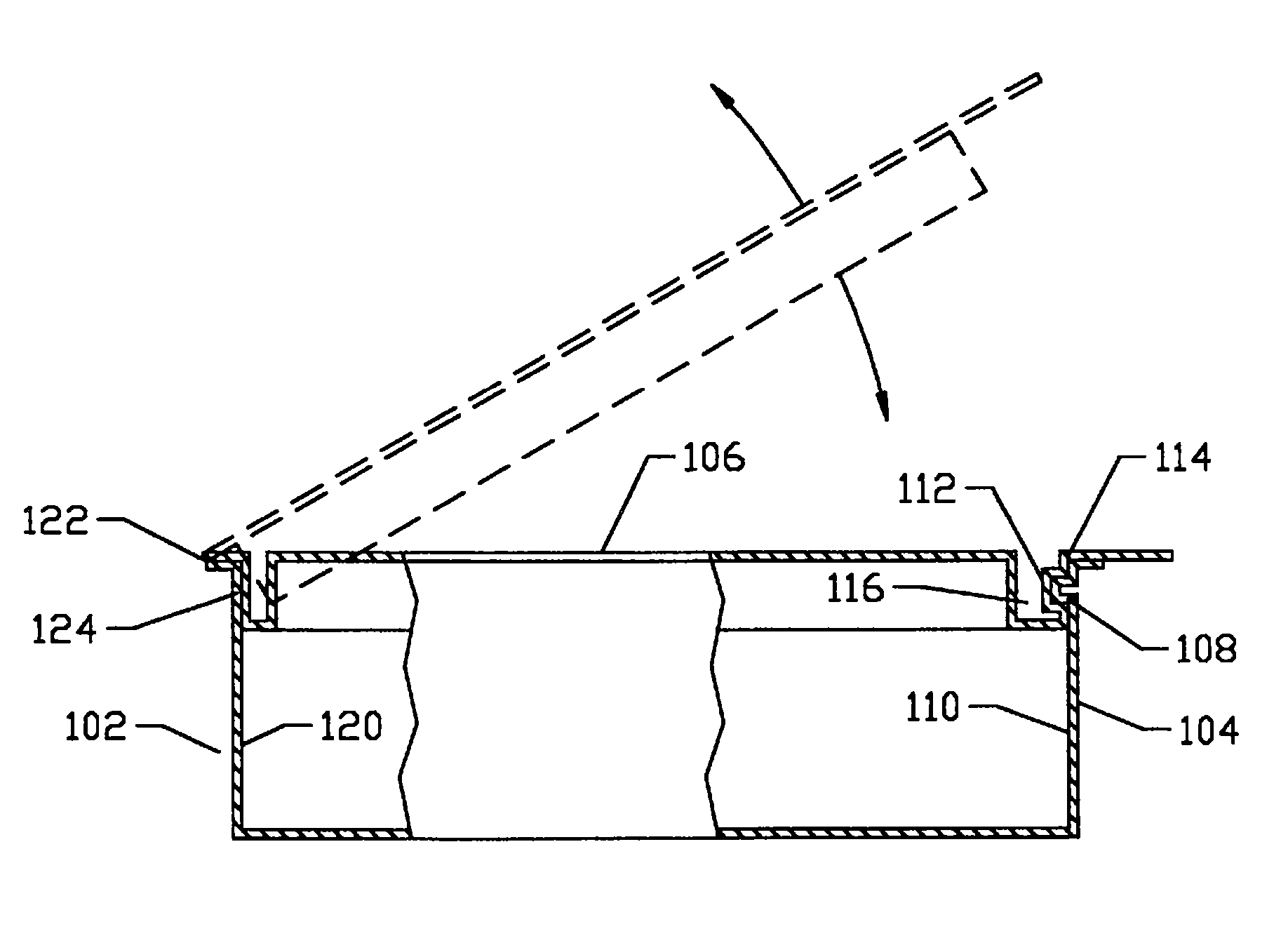
Electromagnetic Interference Shields for Electronic Devices
PatentInactiveUS20070199738A1
Innovation
- A thermoformable polymeric sheet is metallized using vacuum deposition techniques to create a lightweight, conductive enclosure that can be shaped to fit specific components, providing effective EMI shielding with reduced weight and increased design flexibility, and can be easily manufactured and recycled.
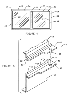
Electromagnetic interference shielding assembly and electronic device having same
PatentInactiveUS20130319751A1
Innovation
- An electromagnetic interference shielding assembly featuring a metallic shielding plate with perpendicular slots is integrated into the electronic device, redirecting induced currents to prevent magnetic field addition and utilizing slot geometry to block electromagnetic waves below their wavelength.
Standards and Compliance Requirements
Electromagnetic Compatibility (EMC) is governed by a comprehensive framework of international, regional, and national standards that manufacturers must adhere to before bringing products to market. The International Electrotechnical Commission (IEC) establishes the foundational EMC standards through its CISPR (International Special Committee on Radio Interference) publications and IEC 61000 series, which define emission limits, immunity requirements, and testing methodologies across various product categories.
In the United States, the Federal Communications Commission (FCC) enforces Part 15 regulations for digital devices, establishing strict limits on radiated and conducted emissions. Similarly, the European Union implements the EMC Directive (2014/30/EU), requiring all electronic equipment sold within member states to demonstrate compliance through CE marking. This directive is supported by harmonized standards like EN 55032 for emissions and EN 55035 for immunity requirements.
Military and aerospace applications face even more stringent requirements under standards such as MIL-STD-461 in the United States and DEF STAN 59-411 in the United Kingdom. These standards specify detailed EMI/EMC requirements for equipment used in defense systems, addressing unique operational environments and mission-critical reliability needs.
The automotive industry follows standards like CISPR 25 and ISO 11452 series, which address the specific challenges of vehicle electronics operating in close proximity. Medical device manufacturers must comply with IEC 60601-1-2, which ensures electromagnetic compatibility in healthcare environments where interference could have life-threatening consequences.
Compliance verification typically involves laboratory testing at accredited facilities, where products undergo a battery of tests including radiated emissions, conducted emissions, electrostatic discharge immunity, and radiated immunity. Documentation requirements include detailed test reports, technical construction files, and declarations of conformity.
The integration of EMI shielding solutions directly addresses these compliance requirements by providing a proactive approach to meeting emission and immunity standards. Properly implemented shielding can significantly reduce the cost and time associated with compliance testing by minimizing the need for design iterations after failed tests. This integration becomes increasingly critical as standards evolve to address higher operating frequencies in modern electronics and more complex electromagnetic environments.
Recent updates to EMC standards have introduced more stringent limits and expanded frequency ranges, reflecting the proliferation of wireless technologies and higher-speed digital circuits. Manufacturers who incorporate comprehensive EMI shielding strategies early in the design process gain a competitive advantage through faster regulatory approval and reduced compliance costs.
Cost-Benefit Analysis of EMI Shielding Solutions
The implementation of EMI shielding solutions requires careful financial consideration to balance effectiveness with economic viability. When evaluating the cost-benefit ratio of various EMI shielding approaches, organizations must consider both direct expenses and long-term value creation.
Initial implementation costs for EMI shielding vary significantly based on the chosen methodology. Basic solutions like conductive paints or tapes typically range from $0.50 to $5 per square foot, while advanced metallic enclosures or specialized composite materials can cost between $10 and $100 per square foot. Custom-designed solutions for complex electronic systems may require substantial engineering investment, potentially adding $10,000 to $50,000 in development costs.
However, these upfront expenditures must be weighed against the substantial benefits and cost avoidance opportunities. Product failure due to electromagnetic interference can result in warranty claims averaging $5,000 to $25,000 per incident for consumer electronics and significantly higher for industrial or medical equipment. Regulatory non-compliance penalties can exceed $100,000 per violation, not including potential legal liabilities.
The return on investment timeline for EMI shielding typically ranges from immediate (in cases where interference issues are preventing product launch) to 12-24 months through reduced field failures and support costs. Companies implementing comprehensive EMI shielding strategies report 15-30% reductions in product returns and 20-40% decreases in technical support requirements related to interference issues.
Integration of EMI shielding during initial design phases, rather than as a retrofit solution, demonstrates particularly favorable economics. Early integration typically adds only 3-8% to component costs while reducing overall development time by eliminating redesign cycles. Conversely, addressing EMI issues after product completion can increase total project costs by 25-75% and delay market entry by 3-6 months.
Emerging technologies like nanomaterial-based shielding solutions offer promising cost-benefit profiles, with initial price premiums of 30-50% compared to traditional methods but delivering 15-25% better attenuation performance and 30-40% weight reduction. These advantages translate to downstream savings in transportation, installation, and operational efficiency that often justify the higher acquisition cost within 18-36 months.
Unlock deeper insights with PatSnap Eureka Quick Research — get a full tech report to explore trends and direct your research. Try now!
Generate Your Research Report Instantly with AI Agent
Supercharge your innovation with PatSnap Eureka AI Agent Platform!