

How EMI Shielding Reduces Electromagnetic Interference in Circuits
SEP 25, 20259 MIN READ
Generate Your Research Report Instantly with AI Agent
PatSnap Eureka helps you evaluate technical feasibility & market potential.
EMI Shielding Background and Objectives
Electromagnetic Interference (EMI) has been a persistent challenge in electronic circuit design since the early days of electronic devices. As electronic systems have evolved from simple circuits to complex integrated systems, the issue of EMI has grown increasingly significant. EMI refers to the unwanted electromagnetic emissions that can disrupt the normal operation of electronic devices, causing performance degradation, data corruption, or even complete system failure.
The historical development of EMI shielding technologies can be traced back to the mid-20th century when military applications first demanded solutions for protecting sensitive electronic equipment from external electromagnetic radiation. The subsequent proliferation of consumer electronics, telecommunications, and computing devices in the latter half of the century further accelerated the need for effective EMI mitigation strategies.
In recent years, the miniaturization of electronic components, increasing clock speeds, and the integration of wireless technologies have dramatically intensified EMI challenges. Modern electronic devices operate at higher frequencies and with lower signal voltages, making them more susceptible to electromagnetic interference. Additionally, the growing density of electronic components within confined spaces has created environments where EMI issues are more likely to occur and more difficult to isolate.
The regulatory landscape has also evolved significantly, with organizations such as the Federal Communications Commission (FCC), International Electrotechnical Commission (IEC), and various national standards bodies establishing increasingly stringent EMI compliance requirements. These regulations aim to ensure that electronic devices neither emit excessive electromagnetic radiation nor are unduly affected by external EMI sources.
The primary objective of EMI shielding technology is to create barriers that prevent electromagnetic waves from either entering or escaping a designated area. This involves the development of materials and designs that can effectively absorb, reflect, or redirect electromagnetic energy without compromising the functionality, cost-effectiveness, or physical characteristics of the electronic system.
Current technological trends in EMI shielding are moving toward more integrated solutions that address EMI concerns at multiple levels: component, board, system, and enclosure. There is also growing interest in developing flexible, lightweight, and environmentally friendly shielding materials that can be easily incorporated into modern electronic designs without adding significant weight, volume, or manufacturing complexity.
Looking forward, the field of EMI shielding aims to develop next-generation solutions capable of addressing the challenges posed by emerging technologies such as 5G communications, Internet of Things (IoT) devices, autonomous vehicles, and advanced medical equipment. These applications demand shielding technologies that can operate effectively across broader frequency ranges while maintaining compatibility with increasingly complex and miniaturized electronic architectures.
Market Demand Analysis for EMI Protection Solutions
The global market for EMI protection solutions has witnessed substantial growth in recent years, driven primarily by the proliferation of electronic devices across various sectors. The increasing density of electronic components in modern circuits has created a pressing need for effective EMI shielding solutions. Market research indicates that the global EMI shielding market was valued at approximately $6.8 billion in 2022 and is projected to reach $9.2 billion by 2027, representing a compound annual growth rate (CAGR) of 6.3%.
Consumer electronics remains the largest application segment, accounting for nearly 35% of the market share. This dominance is attributed to the rising adoption of smartphones, tablets, wearable devices, and other portable electronics that require robust EMI protection to ensure optimal performance. The automotive sector follows closely, with an estimated market share of 28%, as modern vehicles incorporate increasingly sophisticated electronic systems including advanced driver-assistance systems (ADAS), infotainment systems, and electric powertrains.
Healthcare and aerospace & defense sectors are emerging as significant growth areas for EMI shielding solutions. Medical devices, particularly those used in diagnostic imaging and patient monitoring, require high-performance EMI protection to prevent interference with critical functions. The market in these sectors is expected to grow at a CAGR of 7.8% through 2027, outpacing the overall market growth rate.
Regionally, Asia-Pacific dominates the EMI shielding market with approximately 42% share, primarily due to the strong presence of electronics manufacturing hubs in countries like China, Japan, South Korea, and Taiwan. North America and Europe follow with market shares of 27% and 23% respectively, driven by advanced automotive, aerospace, and healthcare industries.
The demand for miniaturized and lightweight EMI shielding solutions is growing significantly as devices become smaller and more portable. This trend has spurred innovation in conductive coatings, flexible shields, and advanced composite materials that offer effective EMI protection without adding substantial weight or volume to the final product.
Environmental regulations are also shaping market demand, with increasing preference for RoHS-compliant and halogen-free EMI shielding materials. This shift is particularly evident in Europe and North America, where stringent environmental standards are enforced. Consequently, manufacturers are investing in developing eco-friendly alternatives to traditional EMI shielding materials containing lead, cadmium, and other hazardous substances.
The increasing adoption of 5G technology presents both challenges and opportunities for the EMI shielding market. The higher frequencies used in 5G communications require more sophisticated shielding solutions to prevent interference, driving demand for advanced EMI protection technologies that can effectively shield against a broader spectrum of electromagnetic frequencies.
Current EMI Shielding Technologies and Challenges
EMI shielding technologies have evolved significantly over the past decades, with various approaches now available to address electromagnetic interference challenges in electronic circuits. Currently, metallic shields remain the most widely implemented solution, with aluminum and copper being predominant materials due to their excellent conductivity and relatively low cost. These shields typically operate through reflection mechanisms, where conductive surfaces redirect electromagnetic waves away from sensitive components.
Conductive coatings represent another major category in contemporary EMI shielding solutions. These include conductive paints, vacuum metallization, and electroless plating techniques that can be applied to plastic enclosures and non-conductive surfaces. While offering flexibility in application, these coatings often face durability challenges and may degrade over time, particularly in harsh environmental conditions.
Advanced composite materials have gained significant traction in recent years, combining polymers with conductive fillers such as carbon nanotubes, graphene, or metal particles. These materials offer the advantage of weight reduction compared to traditional metal shields while maintaining acceptable shielding effectiveness. However, manufacturing consistency and cost remain significant barriers to widespread adoption in consumer electronics.
Gaskets and seals constitute critical components in modern EMI shielding systems, addressing the vulnerability of seams and joints in electronic enclosures. Current technologies include conductive elastomers, metal spring fingers, and wire mesh designs, each offering different trade-offs between compression set resistance, environmental sealing, and shielding effectiveness.
Despite these advancements, several challenges persist in the EMI shielding domain. The continuous miniaturization of electronic devices creates significant spatial constraints for implementing effective shielding solutions. As devices become smaller and more densely packed, traditional shielding approaches become increasingly difficult to implement without compromising device functionality or form factor.
Higher operating frequencies in modern electronics present another substantial challenge. As wireless communications move toward 5G and beyond, operating frequencies extend into millimeter-wave ranges where conventional shielding materials may exhibit reduced effectiveness. This necessitates new material developments and design approaches specifically tailored for high-frequency applications.
Cost-effectiveness remains a persistent challenge, particularly for consumer electronics where price sensitivity is high. Balancing shielding performance with manufacturing costs requires continuous innovation in materials and production processes. Additionally, environmental concerns have prompted research into sustainable shielding materials that can replace traditional options containing heavy metals or environmentally persistent compounds.
Mainstream EMI Shielding Implementation Methods
01 Conductive materials for EMI shielding
Various conductive materials can be used to create effective EMI shields. These include metals like aluminum and copper, conductive polymers, and carbon-based materials such as graphene and carbon nanotubes. These materials create a barrier that blocks or absorbs electromagnetic radiation, preventing it from interfering with electronic components. The conductivity of these materials allows them to reflect or absorb electromagnetic waves, thereby reducing electromagnetic interference.- Conductive materials for EMI shielding: Various conductive materials can be used for electromagnetic interference shielding. These materials include metals, conductive polymers, and carbon-based materials that can effectively block or absorb electromagnetic radiation. The conductivity of these materials allows them to reflect or absorb electromagnetic waves, preventing them from passing through electronic devices and causing interference. These materials can be incorporated into different forms such as coatings, films, or structural components.
- Multilayer shielding structures: Multilayer structures can enhance EMI shielding effectiveness by combining different materials with complementary properties. These structures typically consist of alternating layers of conductive and non-conductive materials, which can provide both reflection and absorption of electromagnetic waves. The layered approach allows for customization of the shielding properties to target specific frequency ranges and provides mechanical stability and environmental protection. Such structures can be designed to meet specific requirements for different electronic applications.
- EMI shielding in electronic enclosures and housings: Electronic enclosures and housings can be designed with integrated EMI shielding features to protect internal components from electromagnetic interference. These designs may include conductive gaskets, coatings, or structural elements that create a Faraday cage effect around sensitive electronics. Proper grounding and sealing of seams and apertures are critical aspects of effective enclosure shielding. Advanced manufacturing techniques allow for the creation of complex shielded enclosures that maintain both electromagnetic protection and thermal management capabilities.
- Flexible and conformal EMI shielding solutions: Flexible and conformal shielding materials provide EMI protection for non-planar surfaces and components with complex geometries. These solutions include conductive fabrics, elastomers, and sprayable coatings that can conform to irregular shapes while maintaining shielding effectiveness. The flexibility of these materials allows for their application in wearable electronics, flexible displays, and other applications where rigid shielding would be impractical. These materials can be designed to maintain their shielding properties even when subjected to bending, stretching, or other mechanical stresses.
- Nanomaterial-based EMI shielding: Nanomaterials such as carbon nanotubes, graphene, and metallic nanoparticles offer advanced EMI shielding properties due to their unique electrical and physical characteristics. These materials can provide effective shielding at lower weight and thickness compared to traditional materials. Nanomaterial-based shields can be incorporated into polymers, coatings, or composites to create lightweight yet effective EMI protection. The high surface area and conductivity of nanomaterials contribute to their superior shielding performance across a wide frequency range.
02 Multilayer shielding structures
Multilayer structures can enhance EMI shielding effectiveness by combining different materials with complementary properties. These structures typically consist of alternating layers of conductive and non-conductive materials, which can provide both reflection and absorption of electromagnetic waves. The layered approach allows for customization of the shielding properties to target specific frequency ranges and can also provide additional benefits such as mechanical strength and environmental protection.Expand Specific Solutions03 EMI shielding for electronic enclosures and housings
Electronic device enclosures and housings can be designed with integrated EMI shielding to protect internal components from external electromagnetic interference and prevent emissions from affecting nearby devices. Techniques include conductive coatings on plastic housings, metal casings with proper grounding, and specialized gaskets at seams and openings. These solutions ensure that the entire device is protected while maintaining functionality, aesthetics, and manufacturing feasibility.Expand Specific Solutions04 Flexible and conformal EMI shielding solutions
Flexible and conformal EMI shielding materials allow for protection of complex geometries and components with irregular shapes. These include conductive fabrics, elastomers, and films that can be applied directly to circuit boards or components. These materials can maintain their shielding effectiveness while being bent, stretched, or compressed, making them ideal for applications where rigid shields would be impractical. They are particularly useful in portable electronics, wearable devices, and applications where space is limited.Expand Specific Solutions05 EMI shielding in high-frequency and high-speed applications
Specialized EMI shielding solutions are required for high-frequency and high-speed electronic applications, such as 5G communications, high-speed data centers, and advanced computing systems. These applications face unique challenges due to the increased potential for interference at higher frequencies. Solutions include advanced composite materials, precisely engineered shield geometries, and specialized grounding techniques. These approaches ensure signal integrity and prevent cross-talk between components while maintaining the performance advantages of high-frequency operation.Expand Specific Solutions
Key Industry Players in EMI Shielding Market
The EMI shielding market is currently in a growth phase, driven by increasing electronic device complexity and miniaturization. The global market size is estimated to reach $9.2 billion by 2026, with a CAGR of approximately 5.8%. Technologically, the field shows varying maturity levels across different applications. Leading players like Intel, Samsung Electronics, and Apple are advancing sophisticated shielding solutions for consumer electronics, while specialized companies such as Laird Technologies and 3M Innovative Properties focus on proprietary materials development. Hon Hai Precision Industry (Foxconn) and Universal Scientific Industrial dominate manufacturing implementation, with Texas Instruments and GLOBALFOUNDRIES integrating shielding directly into semiconductor designs. Research institutions like Virginia Tech Intellectual Properties continue pushing boundaries with next-generation conductive materials and application methods.
Intel Corp.
Technical Solution: Intel has developed sophisticated on-chip EMI shielding technologies for their advanced microprocessors and SoCs. Their approach integrates multiple shielding techniques directly into semiconductor design and packaging. Intel's Embedded Multi-die Interconnect Bridge (EMIB) technology incorporates specialized ground planes and guard rings that isolate sensitive digital circuits from high-frequency analog components. For their latest processors, Intel implements strategic power delivery network (PDN) designs with distributed capacitance to minimize simultaneous switching noise. Their advanced packages utilize copper-filled through-silicon vias (TSVs) arranged in specific patterns to create effective Faraday cage structures around sensitive circuit blocks. Intel's on-die shielding includes metal layers specifically dedicated to EMI containment, with proprietary routing algorithms that optimize signal paths while minimizing electromagnetic coupling. Their testing has shown these integrated approaches can reduce EMI emissions by up to 20dB compared to conventional designs.
Strengths: Deeply integrated solutions that address EMI at the chip design level; comprehensive simulation capabilities that predict EMI issues before manufacturing; solutions optimized for high-performance computing environments. Weaknesses: Technologies primarily developed for Intel's own products; significant expertise required to implement similar approaches in third-party designs; solutions often tied to specific Intel manufacturing processes.
Samsung Electronics Co., Ltd.
Technical Solution: Samsung has pioneered advanced EMI shielding solutions for mobile devices and consumer electronics through their comprehensive "multi-dimensional shielding" approach. Their technology combines wafer-level shielding (WLS), package-level shielding (PLS), and board-level shielding (BLS) to create a hierarchical defense against electromagnetic interference. Samsung's proprietary conformal shielding process applies ultra-thin (under 10μm) metallic layers directly to semiconductor packages using specialized plasma deposition techniques, achieving shielding effectiveness of over 60dB while adding minimal thickness to the overall package. For their flagship mobile devices, Samsung implements resonant cavity shields that create destructive interference patterns for specific problematic frequencies. Their advanced FPCB designs incorporate embedded shielding layers with precisely calculated aperture patterns that block EMI while allowing necessary signal transmission. Samsung has also developed specialized nano-composite materials that combine ferrite particles with polymer matrices, creating flexible shields that can be integrated into curved device housings.
Strengths: Vertical integration allowing for coordinated shielding strategies across components, packages, and systems; extensive manufacturing capabilities supporting high-volume production; solutions optimized for ultra-thin mobile devices. Weaknesses: Some proprietary technologies not available to external customers; highest performance solutions require adoption of Samsung's complete component ecosystem; certain techniques optimized for consumer electronics may not meet industrial or military specifications.
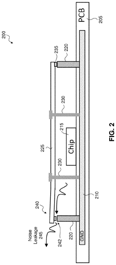
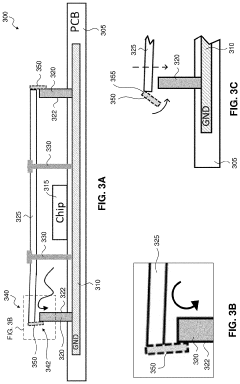
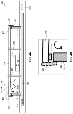
Critical EMI Shielding Materials and Mechanisms
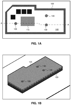
Electromagnetic Interference Shielding for Compact Electronic Devices
PatentInactiveUS20100246143A1
Innovation
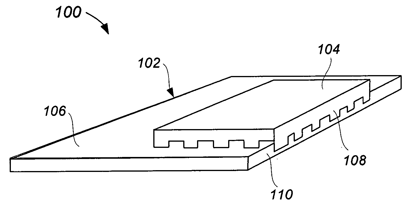
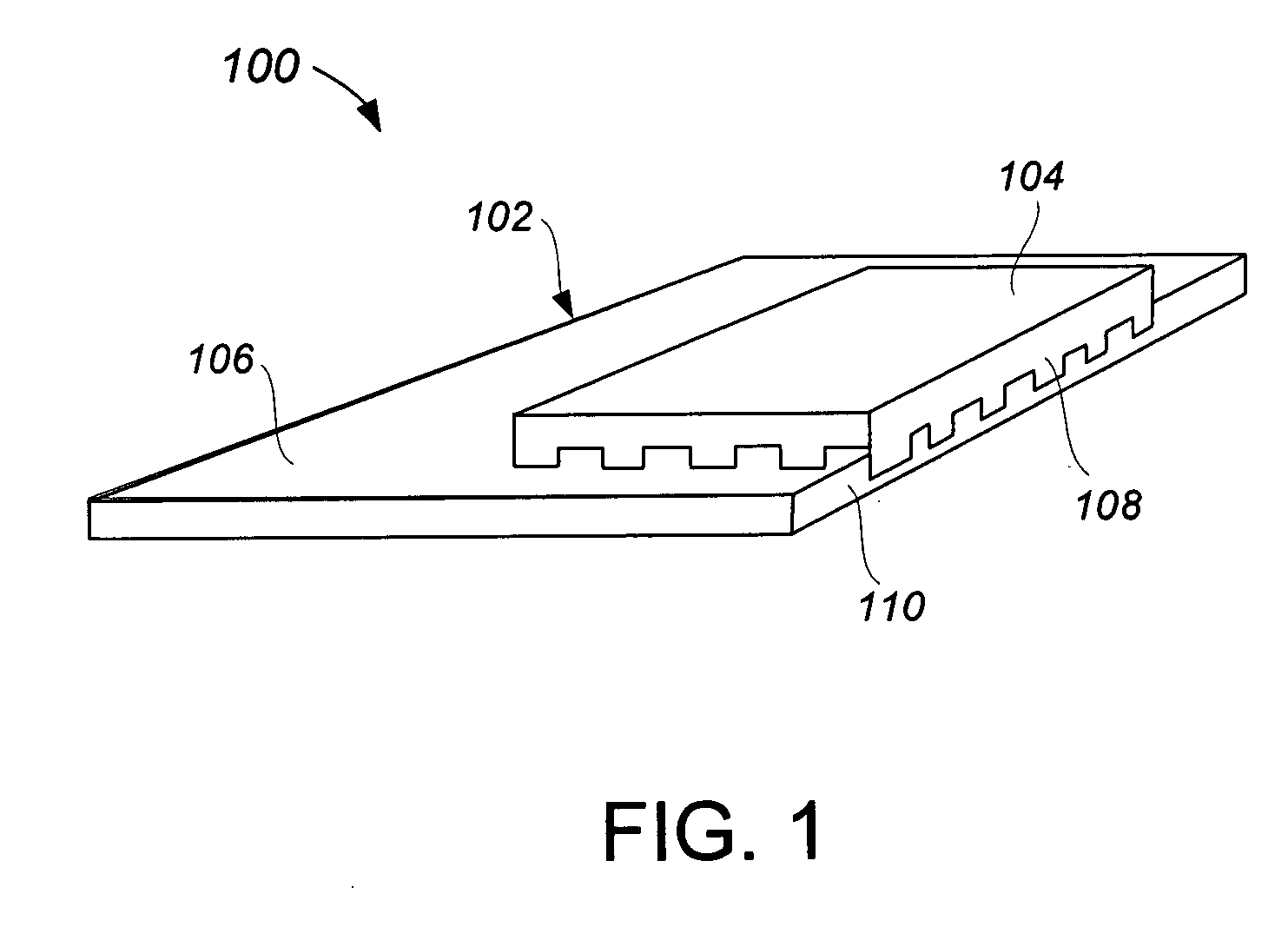
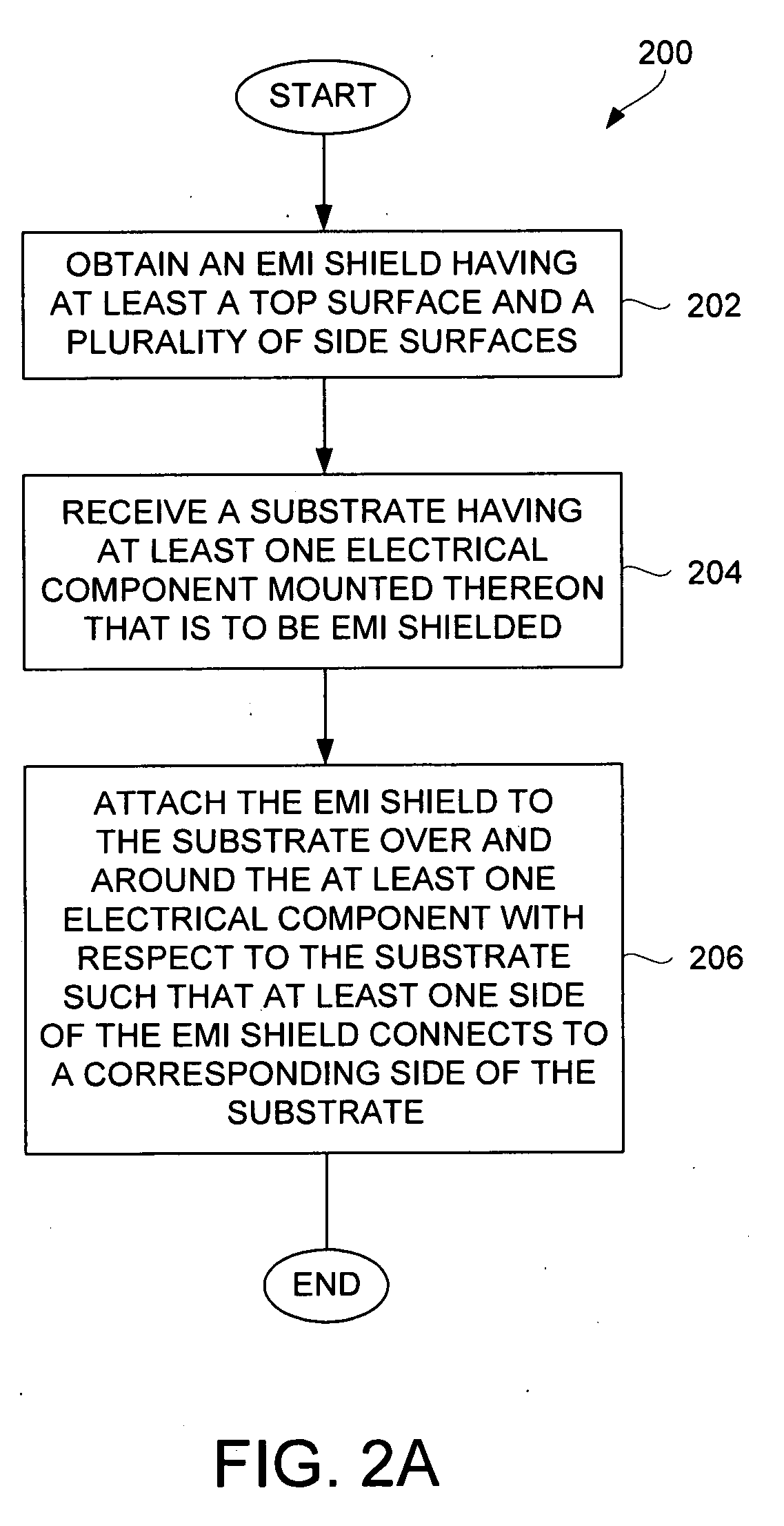
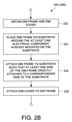
- Attaching an electromagnetic shield to the edges of a substrate, such as a printed circuit board, allows for efficient use of space, enabling wider electrical components without expanding the substrate width, and the shield can be made from conductive materials like sheet metal or mesh, attaching to both surfaces and sides of the substrate.
Electromagnetic interference shielding for a circuit board
PatentActiveUS20200107476A1
Innovation
- The use of magnetized shielding bodies that provide continuous attractive force between shield components without mechanical parts, improving shielding performance, relaxing design specifications, and reducing tooling costs by maintaining magnetism over time.
Regulatory Standards for EMI Compliance
Regulatory standards for EMI compliance form a critical framework that governs electromagnetic compatibility across industries worldwide. The International Electrotechnical Commission (IEC) establishes the foundational standards through IEC 61000 series, which addresses various aspects of electromagnetic compatibility including testing methodologies and immunity requirements. These standards are widely adopted globally and serve as the basis for many regional regulatory frameworks.
In the United States, the Federal Communications Commission (FCC) enforces EMI regulations through Title 47 CFR Part 15, which categorizes devices into Class A (industrial/commercial) and Class B (residential) with corresponding emission limits. The FCC certification process requires comprehensive testing and documentation before products can be marketed, with non-compliance potentially resulting in substantial penalties and market withdrawal.
The European Union implements EMI regulations through the Electromagnetic Compatibility Directive (2014/30/EU), which mandates CE marking for products sold within the European Economic Area. This directive requires manufacturers to demonstrate compliance through technical documentation and appropriate conformity assessment procedures, emphasizing both emissions control and immunity to external interference.
Military and aerospace applications follow more stringent standards such as MIL-STD-461, which specifies detailed requirements for subsystems and equipment used in military platforms. These standards address unique operational environments including high-power radar systems and sensitive communication equipment operating in close proximity.
Automotive industry compliance is governed by standards like CISPR 25 and ISO 11452, which address the specific challenges of vehicle electronics including conducted and radiated emissions. These standards have evolved significantly with the increasing electrification of vehicles and integration of advanced driver assistance systems.
Medical device regulations incorporate EMI considerations through standards like IEC 60601-1-2, recognizing the critical importance of electromagnetic compatibility in healthcare settings where interference could compromise patient safety. These standards mandate rigorous testing to ensure medical devices maintain essential performance under various electromagnetic conditions.
Testing methodologies for compliance verification include open area test sites (OATS), semi-anechoic chambers, and GTEM cells, each offering different advantages for specific measurement scenarios. Accredited testing laboratories issue compliance reports that manufacturers must maintain as part of their technical documentation.
Emerging technologies like 5G, IoT devices, and wireless power transfer systems are driving the evolution of EMI standards, with regulatory bodies continuously updating requirements to address new interference scenarios and higher frequency operations. This dynamic regulatory landscape requires manufacturers to maintain vigilance and adapt their EMI shielding strategies accordingly.
Cost-Benefit Analysis of EMI Shielding Solutions
When evaluating EMI shielding solutions, a comprehensive cost-benefit analysis is essential for making informed implementation decisions. The initial investment in EMI shielding materials and installation represents a significant portion of the total cost. High-performance materials like mu-metal and specialized conductive coatings typically command premium prices, while more common solutions such as aluminum or copper foils offer more economical alternatives with somewhat reduced effectiveness.
Installation complexity substantially impacts overall costs, with custom-designed shields requiring specialized manufacturing processes and skilled labor. Pre-fabricated solutions may reduce these expenses but might not provide optimal performance for specific applications. Additionally, recurring maintenance costs must be factored into long-term financial planning, as certain shielding materials may degrade over time due to environmental factors or mechanical stress.
The benefits side of the equation begins with regulatory compliance. Many industries face strict electromagnetic compatibility (EMC) standards, and implementing appropriate shielding solutions helps avoid costly penalties, product recalls, or market access restrictions. The telecommunications, medical device, and automotive sectors particularly benefit from this compliance assurance.
Product reliability improvements represent another significant benefit. By reducing electromagnetic interference, properly shielded circuits experience fewer operational anomalies, resulting in extended product lifespans and decreased warranty claim expenses. This reliability enhancement directly impacts customer satisfaction and brand reputation, which, while difficult to quantify precisely, carries substantial long-term value.
Performance optimization constitutes a third major benefit category. EMI shielding enables electronic systems to operate at peak efficiency by eliminating signal degradation caused by interference. This optimization can lead to improved data transmission rates, reduced error rates, and enhanced overall system performance—benefits that may justify premium shielding solutions in high-performance applications.
The return on investment timeline varies significantly across applications. Consumer electronics typically require cost-effective solutions with immediate returns, while aerospace or medical equipment can justify more expensive shielding with longer ROI periods due to their critical nature and extended operational lifespans. Quantifying these benefits against implementation costs provides decision-makers with a framework for selecting the most appropriate EMI shielding strategy for their specific technical and business requirements.
Unlock deeper insights with PatSnap Eureka Quick Research — get a full tech report to explore trends and direct your research. Try now!
Generate Your Research Report Instantly with AI Agent
Supercharge your innovation with PatSnap Eureka AI Agent Platform!