

Gallium Nitride Transistor Applications in Modern Electronics
OCT 14, 202510 MIN READ
Generate Your Research Report Instantly with AI Agent
PatSnap Eureka helps you evaluate technical feasibility & market potential.
GaN Transistor Evolution and Development Goals
Gallium Nitride (GaN) transistor technology has undergone remarkable evolution since its inception in the early 1990s. Initially developed as a solution for high-power RF applications in military and aerospace sectors, GaN transistors have progressively expanded into commercial electronics due to their superior performance characteristics compared to silicon-based alternatives. The evolutionary trajectory of GaN transistors has been characterized by continuous improvements in material quality, device architecture, and manufacturing processes.
The first significant milestone in GaN transistor development occurred in 1993 with the demonstration of the first GaN-based high electron mobility transistor (HEMT). This breakthrough was followed by substantial research investments from both government agencies and private corporations seeking to harness GaN's wide bandgap properties. By the early 2000s, researchers had successfully addressed initial challenges related to substrate quality and defect density, enabling the first commercial GaN RF power amplifiers.
Between 2005 and 2015, the focus shifted toward enhancing reliability and reducing production costs. This period saw the introduction of GaN-on-Silicon technology, which significantly lowered manufacturing expenses while maintaining performance advantages. The development of enhanced passivation techniques and advanced thermal management solutions further improved device reliability and operational lifetime.
Recent evolutionary trends have centered on expanding GaN transistor applications beyond RF power amplifiers into power conversion systems. The introduction of enhancement-mode GaN transistors (e-GaN) around 2010 represented a pivotal advancement, enabling simpler gate drive requirements and facilitating broader adoption in consumer electronics and automotive applications.
Current development goals for GaN transistor technology focus on several key areas. First, increasing power density capabilities to enable more compact and efficient power systems remains a primary objective. Engineers are targeting power densities exceeding 10 W/mm² while maintaining reliability standards. Second, reducing the cost of GaN devices to achieve price parity with silicon alternatives represents a critical commercialization goal, with projections suggesting competitive pricing by 2025.
Another significant development target involves improving thermal management solutions to address the high heat flux generated in GaN devices. Research efforts are exploring novel packaging technologies and integration approaches to optimize thermal performance. Additionally, increasing the operating voltage capabilities beyond current 650V limits toward 1200V and higher would enable GaN transistors to penetrate medium-voltage applications currently dominated by silicon carbide devices.
The industry is also pursuing enhanced integration capabilities, with goals to develop GaN-based monolithic integrated circuits that combine power devices with control and protection functions. This integration would significantly reduce system complexity and improve overall performance in applications ranging from data center power supplies to electric vehicle powertrains.
Market Analysis for GaN-Based Electronic Solutions
The global market for Gallium Nitride (GaN) transistor-based electronic solutions has experienced remarkable growth in recent years, driven by increasing demand for high-performance power electronics across multiple sectors. Current market valuations place the GaN power device market at approximately 1.4 billion USD in 2023, with projections indicating a compound annual growth rate (CAGR) of 25% through 2028, potentially reaching 4.3 billion USD by the end of the forecast period.
Consumer electronics represents the largest application segment, accounting for roughly 32% of the total market share. This dominance stems from the integration of GaN transistors in fast chargers, wireless power systems, and high-efficiency power adapters. The automotive sector follows closely at 28% market share, with electric vehicle (EV) manufacturers increasingly adopting GaN-based power conversion systems to enhance charging efficiency and reduce overall vehicle weight.
Telecommunications infrastructure constitutes approximately 18% of the market, primarily through the deployment of GaN-based power amplifiers in 5G base stations. The industrial sector claims about 15% of the market, utilizing GaN solutions for motor drives, industrial power supplies, and renewable energy systems. The remaining 7% is distributed across aerospace, defense, and other specialized applications.
Regional analysis reveals that Asia-Pacific dominates the GaN solutions market with approximately 45% share, attributed to the strong presence of semiconductor manufacturing facilities and consumer electronics production hubs in countries like China, Taiwan, Japan, and South Korea. North America follows with 30% market share, driven by defense applications and technological innovation centers. Europe accounts for 20%, with particular strength in automotive and industrial applications.
Key market drivers include the superior performance characteristics of GaN transistors compared to silicon alternatives, offering higher switching speeds, better thermal performance, and significantly improved power density. The ongoing miniaturization trend in electronics further accelerates adoption, as GaN enables smaller form factors without compromising performance.
Market challenges primarily revolve around cost considerations, with GaN solutions typically commanding a 30-40% premium over silicon alternatives. However, this price differential has been narrowing at approximately 8-10% annually as manufacturing processes mature and economies of scale improve. Technical challenges related to reliability, packaging, and integration with existing systems also present barriers to wider adoption.
The competitive landscape features both established semiconductor giants and specialized GaN-focused startups. Strategic partnerships between device manufacturers and end-product companies have become increasingly common, accelerating the commercialization timeline for new GaN-based solutions.
GaN Technology Status and Implementation Challenges
Gallium Nitride (GaN) technology has emerged as a revolutionary material in the semiconductor industry, offering significant advantages over traditional silicon-based technologies. Currently, GaN transistors have reached commercial maturity in several key application areas, particularly in power electronics and RF communications. The global market has witnessed accelerated adoption of GaN devices, with major semiconductor manufacturers establishing dedicated GaN production lines.
Despite its promising potential, GaN technology faces several implementation challenges that limit its broader adoption. The most significant technical barrier remains the high production cost compared to silicon alternatives, primarily due to complex epitaxial growth processes and substrate compatibility issues. While silicon carbide (SiC) substrates offer better lattice matching for GaN growth, they are substantially more expensive than silicon substrates, creating a cost-performance tradeoff that manufacturers must navigate.
Material quality and defect density represent another critical challenge. The heteroepitaxial growth of GaN on foreign substrates inevitably introduces crystallographic defects that can compromise device performance and reliability. Current defect densities in commercial GaN-on-Si wafers typically range from 10^8 to 10^9 cm^-2, which remains orders of magnitude higher than mature silicon technology.
Thermal management presents a persistent challenge for GaN implementation. Although GaN inherently offers better thermal conductivity than silicon, the high power density capabilities of GaN devices can generate significant localized heating. This necessitates advanced packaging solutions and thermal interface materials to effectively dissipate heat and maintain reliable operation.
Reliability concerns continue to impact widespread GaN adoption, particularly in mission-critical applications. Current-collapse phenomena, gate leakage, and dynamic on-resistance degradation under high-voltage switching conditions remain active areas of research. Industry standards for reliability testing specific to GaN devices are still evolving, creating uncertainty for system designers considering GaN implementation.
From a geographical perspective, GaN technology development shows distinct regional characteristics. Japan and the United States lead in fundamental GaN research and intellectual property, while Taiwan and China have rapidly expanded manufacturing capacity. Europe has established strength in GaN-on-Si technology for power applications, with several research institutes and companies focusing on this approach.
The supply chain for GaN technology remains less mature than silicon, with fewer suppliers for specialized materials, equipment, and processing steps. This creates potential bottlenecks in scaling production and increases dependency on key suppliers. Additionally, design tools and simulation models specifically optimized for GaN device characteristics are still developing, creating challenges for circuit designers transitioning from silicon-based design methodologies.
Current GaN Implementation Architectures and Designs
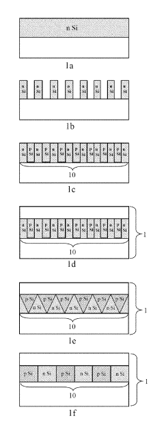
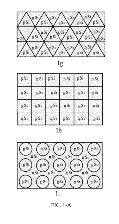
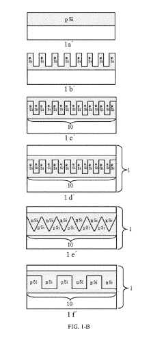
01 Fabrication methods for GaN transistors
Various methods for fabricating gallium nitride transistors have been developed to improve performance and reliability. These methods include specialized deposition techniques, substrate preparation, and layer structuring to enhance electron mobility and reduce defects. Advanced fabrication processes enable the creation of high-quality GaN transistors with improved electrical characteristics and thermal stability for high-power applications.- Fabrication methods for GaN transistors: Various fabrication techniques are employed to create high-quality gallium nitride transistors. These methods include epitaxial growth processes, substrate preparation, and specialized deposition techniques that enhance the crystalline quality of the GaN layers. Advanced manufacturing approaches help reduce defects and improve the overall performance characteristics of the transistors, enabling better electrical properties and reliability.
- GaN HEMT device structures: High Electron Mobility Transistor (HEMT) structures based on gallium nitride offer superior performance for high-power and high-frequency applications. These devices typically feature a two-dimensional electron gas (2DEG) channel formed at the interface between GaN and AlGaN layers. Various structural innovations include field plates, specialized gate configurations, and buffer layer designs that enhance breakdown voltage, reduce leakage current, and improve thermal management.
- GaN substrate and crystal growth technology: The quality of gallium nitride substrates significantly impacts transistor performance. Advanced crystal growth techniques such as hydride vapor phase epitaxy (HVPE), metal-organic chemical vapor deposition (MOCVD), and molecular beam epitaxy (MBE) are used to produce high-quality GaN crystals with minimal defects. These methods address challenges like lattice mismatch and thermal expansion differences when growing GaN on foreign substrates like silicon, sapphire, or silicon carbide.
- GaN power transistor applications: Gallium nitride power transistors offer significant advantages in high-power electronic applications due to their wide bandgap properties. These devices enable more efficient power conversion, higher operating frequencies, and better thermal performance compared to silicon-based alternatives. Applications include power supplies, electric vehicle inverters, RF amplifiers, and renewable energy systems where their high breakdown voltage and low on-resistance provide substantial efficiency improvements.
- GaN transistor reliability and performance enhancement: Improving the reliability and performance of gallium nitride transistors involves addressing specific challenges such as current collapse, dynamic on-resistance, and thermal management. Various techniques include surface passivation, field plate optimization, gate dielectric engineering, and novel device architectures. These enhancements aim to extend device lifetime, improve stability under high-voltage switching conditions, and maximize the inherent advantages of GaN technology.
02 GaN transistor structure and design
Innovative structural designs for gallium nitride transistors focus on optimizing device architecture to maximize performance. These designs include various gate configurations, channel structures, and buffer layer arrangements that enhance electron transport and breakdown voltage. Specific attention is given to heterojunction formations, particularly in high electron mobility transistors (HEMTs), where the interface between different materials significantly impacts device performance.Expand Specific Solutions03 GaN crystal growth and substrate technology
The quality of gallium nitride crystals and substrate materials is crucial for transistor performance. Advanced growth techniques have been developed to produce high-quality GaN crystals with minimal defects and impurities. These methods include modified vapor phase epitaxy, hydride vapor phase epitaxy, and specialized substrate preparation techniques that enable the growth of uniform GaN layers with controlled properties for transistor applications.Expand Specific Solutions04 Power and high-frequency GaN transistor applications
Gallium nitride transistors excel in power electronics and high-frequency applications due to their wide bandgap properties. Specialized designs for power switching applications feature optimized gate structures and field plates to handle high voltages and currents while maintaining efficiency. For RF applications, GaN transistors are engineered with specific channel and contact configurations to operate at high frequencies with minimal signal loss and maximum power output.Expand Specific Solutions05 Enhancement of GaN transistor reliability and performance
Improving the reliability and performance of gallium nitride transistors involves addressing challenges such as current collapse, thermal management, and surface passivation. Various techniques have been developed, including specialized dielectric layers, novel passivation methods, and advanced packaging solutions. These enhancements extend device lifetime, improve stability under high-stress conditions, and optimize electrical characteristics for demanding applications.Expand Specific Solutions
Leading GaN Semiconductor Manufacturers and Competitors
Gallium Nitride (GaN) transistor technology is rapidly transforming modern electronics, currently in a growth phase characterized by expanding applications and increasing market adoption. The global GaN power device market is projected to reach significant scale, driven by advantages in power efficiency and switching speed over traditional silicon. Technology maturity varies across players, with companies like GaN Systems, Transphorm, and Navitas Semiconductor leading in commercialization of GaN-based power solutions. Established semiconductor giants including NXP, Infineon, and Taiwan Semiconductor Manufacturing Co. are investing heavily in GaN technology integration. Research institutions such as Xidian University and the University of California are advancing fundamental innovations, while companies like MACOM and Analog Devices focus on specialized RF applications, collectively accelerating industry-wide adoption.
GaN Systems, Inc.
Technical Solution: GaN Systems has developed a comprehensive portfolio of gallium nitride power transistors specifically designed for high-efficiency power conversion applications. Their Island Technology® die design, combined with GaNPX® packaging, enables high current, high voltage breakdown, and optimal thermal performance. The company's transistors feature low inductance, low thermal resistance, and a small footprint that significantly reduces switching losses. Their GaN E-HEMTs (Enhancement-mode High Electron Mobility Transistors) operate at switching frequencies up to 100 MHz, enabling power density improvements of up to 4x compared to silicon solutions. GaN Systems has also developed proprietary GaNPX packaging technology that eliminates wire bonds and provides superior thermal performance, allowing their transistors to operate reliably at junction temperatures up to 175°C while maintaining excellent switching characteristics.
Strengths: Superior power density (4x over silicon), extremely high switching speeds (up to 100 MHz), and excellent thermal management through innovative packaging. Weaknesses: Higher cost compared to silicon alternatives, requires specialized gate drivers, and has more complex design considerations for optimal performance.
Transphorm Technology, Inc.
Technical Solution: Transphorm specializes in high-voltage GaN power conversion devices based on their patented two-dimensional electron gas (2DEG) technology. Their GaN FETs utilize a cascode configuration that combines a low-voltage silicon MOSFET with a high-voltage GaN HEMT, allowing the devices to be driven with standard silicon gate drivers. This approach enables easier adoption in existing silicon-based designs. Transphorm's devices feature breakdown voltages of 650V and 900V, making them suitable for higher voltage applications like power supplies, motor drives, and renewable energy systems. Their SuperGaN® technology delivers lower on-resistance and reduced switching losses, achieving efficiencies exceeding 99% in power conversion applications. Transphorm has also developed robust qualification procedures that exceed JEDEC standards, addressing reliability concerns that have historically limited GaN adoption in mission-critical applications.
Strengths: High voltage capability (up to 900V) suitable for industrial applications; compatibility with standard silicon gate drivers enabling easier adoption; extensive reliability testing and qualification. Weaknesses: Cascode configuration introduces some additional parasitic elements compared to pure enhancement-mode designs; slightly lower switching speed than some competing GaN technologies.
Key GaN Transistor Patents and Technical Innovations
Nitride power transistor and manufacturing method thereof
PatentActiveUS20190140088A1
Innovation
- A nitride power transistor is developed with a silicon substrate featuring a differently doped semiconductor composite structure forming a space charge depletion region, combined with a nitride epitaxial layer, which increases the breakdown voltage and includes a GaN capping layer and AlN insertion layer to enhance electron mobility and reduce surface defects.
Gallium nitride material transistors and methods for wideband applications
PatentInactiveUS20070202360A1
Innovation
- The development of gallium nitride material transistors with active regions formed in gallium nitride layers, integrated with matching circuits to achieve low relative constellation error (RCE) values and high efficiency, enabling efficient signal amplification and transmission with excellent linearity and compliance with spectrum mask requirements.
Thermal Management Solutions for GaN-Based Systems
Thermal management represents one of the most critical challenges in the widespread adoption of Gallium Nitride (GaN) transistor technology. Despite GaN's superior performance characteristics, these devices generate significant heat during operation due to their high power density capabilities. The thermal conductivity of GaN (approximately 130 W/m·K) is notably lower than silicon carbide (SiC), creating inherent thermal dissipation challenges that must be addressed through innovative cooling solutions.
Current thermal management approaches for GaN-based systems can be categorized into passive and active cooling methodologies. Passive cooling techniques include advanced thermal interface materials (TIMs) with enhanced thermal conductivity exceeding 5 W/m·K, specialized heat spreaders utilizing diamond-copper composites, and optimized PCB designs featuring thermal vias and embedded heat pipes. These passive solutions offer reliability advantages through their lack of moving parts and reduced maintenance requirements.
Active cooling technologies have evolved significantly to address GaN's thermal demands. Microfluidic cooling channels integrated directly into GaN device packaging have demonstrated the ability to handle heat fluxes exceeding 1000 W/cm². Two-phase cooling systems utilizing dielectric fluids show particular promise, achieving junction temperature reductions of up to 40°C compared to conventional air cooling in high-power RF applications.
Advanced thermal simulation tools have become essential in GaN thermal management, with multi-physics modeling platforms enabling accurate prediction of hotspot formation and thermal gradients. These computational approaches allow designers to optimize thermal solutions before physical prototyping, significantly reducing development cycles and improving reliability predictions.
Material innovations continue to drive improvements in GaN thermal management. Graphene-enhanced TIMs have demonstrated thermal conductivity improvements of 45% over traditional materials. Meanwhile, ceramic-based substrates with embedded cooling channels offer both electrical isolation and enhanced thermal performance for GaN power devices operating at high voltages.
Industry standardization efforts are underway to establish consistent thermal characterization methodologies for GaN devices. The JEDEC JC-15 committee has developed specific guidelines for thermal testing of wide bandgap semiconductors, addressing the unique challenges of accurately measuring junction temperatures in these high-power density applications.
Looking forward, emerging technologies such as additive manufacturing of complex 3D cooling structures and integration of phase-change materials directly into GaN packaging represent promising directions for next-generation thermal management solutions. These approaches aim to address the increasing thermal demands as GaN devices continue to push power density boundaries in applications ranging from 5G infrastructure to electric vehicle power conversion systems.
Sustainability Impact of GaN Technology Adoption
The adoption of Gallium Nitride (GaN) technology represents a significant shift toward more sustainable electronics manufacturing and operation. GaN transistors require substantially less energy during operation compared to traditional silicon-based alternatives, with efficiency improvements ranging from 40% to 95% depending on the application. This dramatic reduction in energy consumption translates directly to lower carbon emissions across the product lifecycle, particularly in power-intensive applications such as data centers and electric vehicle charging infrastructure.
Manufacturing processes for GaN components have evolved to require fewer toxic chemicals and generate less hazardous waste than conventional semiconductor fabrication. Recent industry reports indicate that GaN production can reduce harmful chemical usage by up to 30% while decreasing water consumption by approximately 25% compared to silicon semiconductor manufacturing. These improvements address critical environmental concerns in the notoriously resource-intensive semiconductor industry.
The extended operational lifespan of GaN devices further enhances their sustainability profile. With superior thermal performance and resistance to electrical stress, GaN transistors typically last 3-5 times longer than silicon equivalents in high-stress applications. This longevity reduces electronic waste generation and decreases the environmental impact associated with manufacturing replacement components.
Material efficiency represents another sustainability advantage of GaN technology. The higher power density of GaN allows for smaller device footprints, reducing raw material requirements by up to 60% in some applications. This miniaturization cascades through the supply chain, decreasing packaging materials, shipping weight, and ultimately transportation-related emissions.
In renewable energy systems, GaN transistors enable more efficient power conversion, improving solar inverter efficiency by 2-3 percentage points and wind power conversion systems by similar margins. These seemingly modest improvements translate to significant energy capture gains when deployed at scale, accelerating the transition to renewable energy sources.
The circular economy potential of GaN technology is beginning to emerge as manufacturers develop recycling processes specific to these materials. While still in early stages, research indicates that up to 85% of the gallium in end-of-life GaN devices could potentially be recovered and reused, creating a more sustainable material cycle than currently possible with conventional semiconductor technologies.
As regulatory frameworks increasingly emphasize environmental performance, GaN technology positions adopters favorably for compliance with emerging standards such as the EU's Eco-design Directive and various global carbon reduction initiatives. This regulatory alignment provides both environmental benefits and strategic advantages for companies investing in GaN-based solutions.
Unlock deeper insights with PatSnap Eureka Quick Research — get a full tech report to explore trends and direct your research. Try now!
Generate Your Research Report Instantly with AI Agent
Supercharge your innovation with PatSnap Eureka AI Agent Platform!