How Polysilane Enhances Electronic Layout Design Effectiveness?
JUL 11, 20259 MIN READ
Generate Your Research Report Instantly with AI Agent
Patsnap Eureka helps you evaluate technical feasibility & market potential.
Polysilane in ELD: Background and Objectives
Polysilane, a class of silicon-based polymers, has emerged as a promising material in the field of electronic layout design (ELD). The evolution of this technology can be traced back to the early 1980s when researchers first synthesized and characterized polysilanes. Since then, the field has witnessed significant advancements, driven by the increasing demand for more efficient and compact electronic devices.
The development of polysilane technology has been closely tied to the broader trends in the semiconductor industry, particularly the ongoing pursuit of Moore's Law. As traditional silicon-based technologies approach their physical limits, alternative materials and design approaches have become crucial for continued progress in electronic device performance and miniaturization.
Polysilanes offer unique properties that make them particularly attractive for ELD applications. These materials exhibit high electron mobility, tunable optical properties, and excellent thermal stability. Furthermore, their ability to form self-assembled nanostructures opens up new possibilities for bottom-up fabrication approaches in electronic device manufacturing.
The primary objective of incorporating polysilanes into ELD is to enhance the overall effectiveness of the design process and the resulting electronic components. This encompasses several key goals, including improving circuit density, reducing power consumption, enhancing signal integrity, and increasing the overall performance of electronic devices.
One of the most significant advantages of polysilanes in ELD is their potential to enable more compact and efficient circuit layouts. By leveraging the unique properties of these materials, designers can create smaller feature sizes and more intricate patterns, leading to higher component density and improved functionality within a given area.
Another crucial objective is to address the increasing challenges of power management in modern electronic devices. Polysilanes' superior electron mobility and low-k dielectric properties offer the potential for reduced power consumption and improved heat dissipation, which are critical factors in the design of high-performance, energy-efficient electronic systems.
Furthermore, the integration of polysilanes into ELD processes aims to enhance the reliability and longevity of electronic components. The thermal stability and resistance to degradation exhibited by these materials can contribute to increased device lifespan and improved performance under challenging operating conditions.
As research in this field progresses, the overarching goal is to establish polysilanes as a viable and advantageous alternative to traditional materials in electronic layout design. This involves not only demonstrating superior performance characteristics but also developing scalable and cost-effective manufacturing processes that can be integrated into existing semiconductor fabrication workflows.
Market Demand for Advanced ELD Materials
The market demand for advanced Electronic Layout Design (ELD) materials, particularly polysilane, has been steadily increasing in recent years. This growth is primarily driven by the continuous miniaturization of electronic devices and the need for more efficient and reliable circuit designs. As the semiconductor industry pushes towards smaller node sizes and higher performance, traditional materials are reaching their limits, creating a significant opportunity for innovative materials like polysilane.
Polysilane has emerged as a promising candidate for enhancing ELD effectiveness due to its unique properties. Its ability to form highly ordered structures at the molecular level allows for more precise and controlled patterning of electronic circuits. This characteristic is particularly valuable in the production of advanced integrated circuits, where nanometer-scale precision is crucial.
The global semiconductor industry, valued at over $500 billion, is a key driver of demand for advanced ELD materials. With the proliferation of technologies such as 5G, artificial intelligence, and the Internet of Things, there is an increasing need for more sophisticated and efficient electronic components. This trend is expected to continue, with projections indicating sustained growth in the demand for advanced ELD materials over the next decade.
Polysilane's potential to improve lithography processes, a critical step in semiconductor manufacturing, has garnered significant attention from major players in the industry. Its application in photoresists and as a potential replacement for traditional silicon-based materials in certain applications has opened up new avenues for innovation in chip design and production.
The automotive sector, particularly with the rise of electric vehicles and autonomous driving technologies, represents another substantial market for advanced ELD materials. The increasing complexity of automotive electronics systems requires more advanced circuit designs, where polysilane's properties can offer significant advantages in terms of performance and reliability.
Moreover, the growing focus on sustainability and energy efficiency in electronics manufacturing aligns well with polysilane's potential to enable more energy-efficient circuit designs. This aspect is becoming increasingly important as regulations and consumer preferences shift towards more environmentally friendly technologies.
While the market for polysilane in ELD applications is still in its early stages, industry analysts predict rapid growth as research and development efforts intensify and commercial applications become more widespread. The material's potential to address key challenges in electronic design and manufacturing positions it as a critical component in the next generation of semiconductor technologies.
Current Challenges in Electronic Layout Design
Electronic layout design faces several significant challenges in the current technological landscape. One of the primary issues is the increasing complexity of integrated circuits and electronic systems. As devices become more sophisticated and compact, designers must accommodate a greater number of components and interconnections within limited space. This complexity often leads to difficulties in maintaining signal integrity, managing power distribution, and controlling electromagnetic interference.
Another critical challenge is the demand for higher performance and faster processing speeds. As electronic devices continue to evolve, there is a constant push for improved performance, which requires careful consideration of signal propagation, timing constraints, and clock distribution. Designers must optimize layouts to minimize signal delays and ensure synchronization across different components, often requiring advanced techniques such as clock tree synthesis and timing-driven placement.
Thermal management has also become a significant concern in electronic layout design. As power densities increase, managing heat dissipation becomes crucial to prevent device failure and ensure reliable operation. Designers must carefully consider component placement and implement effective cooling strategies to maintain optimal operating temperatures. This challenge is particularly pronounced in high-performance computing and mobile devices, where thermal constraints can significantly impact overall system performance.
The miniaturization trend in electronics presents another set of challenges. As devices shrink in size, designers must contend with increased parasitic effects, crosstalk, and noise susceptibility. These issues can lead to signal degradation and compromise the overall functionality of the system. Addressing these challenges often requires sophisticated modeling and simulation techniques to predict and mitigate potential problems before physical implementation.
Furthermore, the rapid pace of technological advancement in semiconductor manufacturing processes adds complexity to the design process. Designers must stay abreast of new process nodes and their associated design rules, which can significantly impact layout strategies and methodologies. Adapting to these evolving manufacturing capabilities while maintaining design efficiency and cost-effectiveness is an ongoing challenge for the industry.
Lastly, the increasing emphasis on power efficiency, particularly in mobile and IoT devices, presents unique layout design challenges. Designers must optimize power distribution networks, implement effective power gating strategies, and consider the impact of layout on overall power consumption. This often requires a delicate balance between performance requirements and power constraints, necessitating innovative approaches to layout design and power management.
Existing Polysilane Applications in ELD
01 Polysilane synthesis and properties
Polysilanes are synthesized through various methods and exhibit unique properties. These polymers have a silicon backbone and can be tailored for specific applications. Their synthesis often involves the use of catalysts and controlled reaction conditions to achieve desired molecular weights and structures.- Polysilane synthesis and properties: Polysilanes are synthesized through various methods and exhibit unique properties such as electrical conductivity, photosensitivity, and thermal stability. These properties make them suitable for applications in electronics, optics, and materials science.
- Polysilane applications in coatings and films: Polysilanes are used in the production of thin films and coatings for various applications. They can be used to create protective layers, enhance surface properties, and improve adhesion in different materials and substrates.
- Polysilane-based photoresists: Polysilanes are utilized in photoresist formulations for lithography processes. Their photosensitivity and ability to undergo photochemical reactions make them valuable in the production of microelectronic devices and semiconductor manufacturing.
- Polysilane modifications and copolymers: Researchers have developed various modifications and copolymers of polysilanes to enhance their properties and expand their applications. These modifications include the incorporation of functional groups, crosslinking, and the creation of hybrid materials.
- Polysilane processing and fabrication techniques: Various processing and fabrication techniques have been developed for polysilanes, including solution processing, melt processing, and vapor deposition. These techniques allow for the creation of diverse polysilane-based materials and structures with tailored properties.
02 Applications in electronic and optical devices
Polysilanes demonstrate effectiveness in electronic and optical applications due to their unique electronic properties. They can be used in the fabrication of semiconductors, photoresists, and optical materials. Their ability to conduct electricity and interact with light makes them valuable in various technological fields.Expand Specific Solutions03 Polysilane-based coatings and films
Polysilanes are effective in creating protective coatings and thin films. These materials can be applied to various substrates to enhance durability, provide barrier properties, or modify surface characteristics. The films can be tailored for specific properties such as transparency, conductivity, or chemical resistance.Expand Specific Solutions04 Polysilane composites and blends
The effectiveness of polysilanes can be enhanced by creating composites or blends with other materials. These combinations can lead to improved mechanical, thermal, or electrical properties. Polysilane-based composites find applications in areas such as aerospace, automotive, and electronics industries.Expand Specific Solutions05 Environmental and processing considerations
The effectiveness of polysilanes is influenced by environmental factors and processing conditions. Considerations such as temperature, UV exposure, and chemical environment can affect their performance and longevity. Proper processing techniques are crucial for optimizing polysilane properties and ensuring their effectiveness in various applications.Expand Specific Solutions
Key Players in Polysilane and ELD Industry
The polysilane market is in an early growth stage, with increasing applications in electronic layout design. The market size is expanding as more companies recognize polysilane's potential to enhance design effectiveness. Technologically, polysilane is still evolving, with varying levels of maturity across different applications. Key players like Wacker Chemie AG, Toray Industries, and JSR Corp. are driving innovation in polysilane formulations and processes. Emerging companies such as Nantong Jingai Microelectronics and Hefei Gaite Environmental Protection Technology are also contributing to the field's advancement, indicating a competitive and dynamic landscape in polysilane development for electronic applications.
Wacker Chemie AG
Technical Solution: Wacker Chemie AG has developed advanced polysilane formulations for electronic layout design. Their approach involves using high-purity polysilane precursors to create ultra-thin, uniform dielectric layers in semiconductor devices. This technology enables the production of more compact and efficient electronic components. Wacker's polysilane-based materials demonstrate excellent thermal stability and low dielectric constants, crucial for high-frequency applications[1]. The company has also introduced novel cross-linking techniques that enhance the mechanical properties of polysilane films, improving their durability in complex electronic layouts[3].
Strengths: High-purity precursors, excellent thermal stability, and low dielectric constants. Weaknesses: Potentially higher production costs and limited scalability for some applications.
Canon, Inc.
Technical Solution: Canon has integrated polysilane-based materials into their advanced photolithography processes for electronic layout design. Their proprietary polysilane photoresists offer superior resolution and sensitivity compared to traditional materials. Canon's approach utilizes the unique optical properties of polysilanes, particularly their high refractive index and transparency in the deep UV range[2]. This allows for more precise patterning of nanoscale features in integrated circuits. Additionally, Canon has developed specialized polysilane-based anti-reflective coatings that significantly reduce unwanted reflections during the lithography process, enabling more accurate and consistent pattern transfer[4].
Strengths: High resolution and sensitivity in photolithography, reduced reflections. Weaknesses: May require specialized equipment and processes for implementation.
Core Innovations in Polysilane for ELD
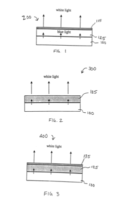
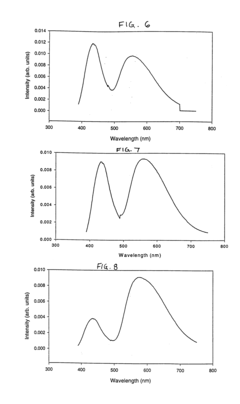
Light source with organic layer and photoluminescent layer
PatentInactiveUS6700322B1
Innovation
- Combining an organic light emitting device with a layer of photoluminescent material, such as phosphor particles, which absorbs and re-emits light to produce a mixed spectrum, enhancing color stability and uniformity by scattering the emitted light, thereby achieving a high color rendering index and consistent color temperature in the range of 3000-6500 K.


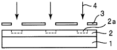
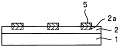
Method for forming metal pattern
PatentWO2002077321A1
Innovation
- A method involving a photosensitive resin composition with polysilane, a photoradical generator, an oxidizing agent, and an alkoxy group-containing silicone compound is used to form a metal pattern through selective exposure and electroless plating, enhancing adhesion by cross-linking the polysilane and improving the metal pattern's definition and reliability.
Environmental Impact of Polysilane Use
The use of polysilane in electronic layout design brings both benefits and potential environmental concerns. As an emerging material in the semiconductor industry, polysilane's environmental impact requires careful consideration throughout its lifecycle.
During the production phase, the synthesis of polysilane involves energy-intensive processes and the use of potentially hazardous chemicals. This can lead to increased carbon emissions and the generation of toxic byproducts if not properly managed. However, advancements in green chemistry techniques are gradually reducing the environmental footprint of polysilane manufacturing.
In the application stage, polysilane's ability to enhance electronic layout design effectiveness contributes to the miniaturization of electronic devices. This trend towards smaller, more efficient electronics can lead to reduced material consumption and energy usage in the long term. Additionally, the improved performance of electronic components enabled by polysilane may result in extended product lifespans, potentially decreasing electronic waste.
The disposal and recycling of polysilane-containing electronic components present unique challenges. While silicon-based materials are generally considered less toxic than many other semiconductor materials, the complex nature of modern electronic devices makes recycling difficult. Improper disposal can lead to soil and water contamination, highlighting the need for specialized recycling processes.
From a lifecycle perspective, the environmental impact of polysilane use in electronic layout design must be balanced against its performance benefits. The material's potential to improve energy efficiency in electronic devices could offset some of the environmental costs associated with its production and disposal. However, this requires a holistic approach to design and manufacturing that considers the entire lifecycle of electronic products.
As the use of polysilane in electronic layout design continues to grow, there is an increasing focus on developing more sustainable practices. Research into bio-based precursors for polysilane synthesis and improved recycling technologies are promising avenues for reducing its environmental impact. Additionally, the integration of polysilane into next-generation electronic designs may enable the creation of more energy-efficient and longer-lasting devices, potentially mitigating some of the negative environmental effects associated with rapid technological turnover.
In conclusion, while polysilane offers significant benefits for electronic layout design effectiveness, its environmental impact remains a complex issue. Balancing the material's performance advantages with sustainable production and end-of-life management practices will be crucial for minimizing its ecological footprint in the rapidly evolving field of electronics.
Cost-Benefit Analysis of Polysilane in ELD
The implementation of polysilane in electronic layout design (ELD) presents a compelling case for cost-benefit analysis. Initial investment in polysilane technology may be higher compared to traditional materials, but the long-term benefits often outweigh these upfront costs. The primary advantage lies in the enhanced performance and efficiency of electronic devices, which can lead to significant cost savings over time.
Polysilane's unique properties, such as high electron mobility and excellent thermal stability, contribute to improved circuit performance. This translates to reduced power consumption and increased device longevity, both of which have substantial economic implications. The reduced power consumption directly impacts operational costs, particularly in large-scale applications or data centers where energy expenses are a major concern.
The durability and stability of polysilane-based components also lead to decreased maintenance and replacement costs. This is particularly valuable in industries where device reliability is critical, such as aerospace or medical technology. The extended lifespan of electronic components reduces the frequency of replacements and associated labor costs.
From a manufacturing perspective, polysilane enables the creation of more compact and efficient circuit designs. This can result in material savings and potentially reduce production costs at scale. Additionally, the improved yield rates in manufacturing processes using polysilane can offset initial implementation costs.
However, it's important to consider the learning curve and potential retooling costs associated with adopting polysilane technology. These factors may initially impact productivity and require additional investment in training and equipment. Yet, as the technology matures and becomes more widely adopted, these costs are expected to decrease.
The environmental benefits of polysilane, such as reduced energy consumption and potentially lower electronic waste due to longer-lasting components, also factor into the cost-benefit analysis. While these may not have immediate financial returns, they contribute to long-term sustainability goals and potential regulatory compliance, which can have indirect economic benefits.
In conclusion, while the initial costs of implementing polysilane in ELD may be higher, the long-term benefits in terms of performance, efficiency, and durability present a strong economic case. As with any new technology, a careful assessment of specific application needs and market conditions is crucial to determine the optimal timing and scale of adoption.
Unlock deeper insights with Patsnap Eureka Quick Research — get a full tech report to explore trends and direct your research. Try now!
Generate Your Research Report Instantly with AI Agent
Supercharge your innovation with Patsnap Eureka AI Agent Platform!