How Polysilane Reduces Energy Loss in Semiconductor Devices?
JUL 11, 20259 MIN READ
Generate Your Research Report Instantly with AI Agent
Patsnap Eureka helps you evaluate technical feasibility & market potential.
Polysilane Background
Polysilane, a class of silicon-based polymers, has emerged as a promising material in the field of semiconductor devices due to its unique electronic properties and potential to reduce energy loss. The history of polysilane research dates back to the 1920s when the first synthesis of these materials was reported. However, it wasn't until the 1980s that their potential in electronic applications began to be fully explored.
Polysilanes are characterized by their backbone structure consisting of silicon atoms bonded to organic side groups. This structure gives rise to their distinctive electronic properties, including high electron mobility and strong absorption in the ultraviolet region. These characteristics make polysilanes particularly interesting for applications in semiconductor devices, where energy efficiency is a critical concern.
The development of polysilanes has been driven by the need for more efficient and environmentally friendly electronic materials. As traditional silicon-based semiconductors approach their physical limits, researchers have turned to alternative materials to overcome these limitations. Polysilanes offer several advantages in this regard, including their ability to be processed at lower temperatures and their potential for solution-based deposition methods.
One of the key features of polysilanes that contributes to their potential in reducing energy loss is their unique electronic structure. The delocalized σ-electrons along the silicon backbone allow for efficient charge transport, potentially leading to lower resistance and reduced energy dissipation in electronic devices. This property has sparked interest in using polysilanes as charge transport layers in various semiconductor applications, including solar cells and light-emitting diodes.
The evolution of polysilane research has seen significant advancements in synthesis methods and the development of various types of polysilanes with tailored properties. From simple linear polysilanes to more complex branched and network structures, researchers have expanded the range of available materials to suit different applications. This diversity allows for fine-tuning of electronic properties to meet specific device requirements and optimize energy efficiency.
Recent years have witnessed an increased focus on incorporating polysilanes into hybrid organic-inorganic semiconductor systems. These hybrid materials aim to combine the best properties of both organic and inorganic components, potentially leading to devices with superior performance and reduced energy loss. The integration of polysilanes into such systems represents a promising direction for future research and development in the field of energy-efficient semiconductor devices.
Market for Energy-Efficient Semiconductors
The market for energy-efficient semiconductors has been experiencing significant growth in recent years, driven by the increasing demand for devices with lower power consumption and improved performance. This trend is particularly evident in the consumer electronics, automotive, and industrial sectors, where energy efficiency has become a critical factor in product design and development.
In the consumer electronics market, smartphones, tablets, and wearable devices are key drivers for energy-efficient semiconductors. As these devices become more powerful and feature-rich, manufacturers are constantly seeking ways to extend battery life and reduce heat generation. This has led to a surge in demand for low-power processors, memory chips, and other semiconductor components that can deliver high performance while minimizing energy consumption.
The automotive industry is another major market for energy-efficient semiconductors, particularly with the rise of electric and hybrid vehicles. These vehicles require advanced power management systems and efficient motor control circuits to maximize range and performance. Additionally, the increasing integration of advanced driver assistance systems (ADAS) and infotainment features in modern vehicles has created a need for energy-efficient processors and sensors that can operate reliably in automotive environments.
In the industrial sector, the adoption of Internet of Things (IoT) technologies and smart manufacturing processes has fueled demand for energy-efficient semiconductors. Industrial automation systems, sensors, and control devices require low-power components to enable long-term operation and reduce overall energy costs in manufacturing facilities.
The data center and cloud computing markets are also significant consumers of energy-efficient semiconductors. As the volume of data processed and stored continues to grow exponentially, data center operators are increasingly focused on reducing power consumption and improving energy efficiency to lower operating costs and meet sustainability goals.
The market for energy-efficient semiconductors is highly competitive, with major players such as Intel, AMD, NVIDIA, and Qualcomm investing heavily in research and development to improve the energy efficiency of their products. This competition has led to rapid advancements in semiconductor design and manufacturing processes, resulting in continuous improvements in power efficiency across a wide range of devices and applications.
As environmental concerns and energy costs continue to drive the adoption of more efficient technologies, the market for energy-efficient semiconductors is expected to maintain its growth trajectory in the coming years. This presents significant opportunities for semiconductor manufacturers and device makers to innovate and differentiate their products based on energy efficiency metrics.
Current Challenges in Semiconductor Energy Efficiency
The semiconductor industry faces significant challenges in improving energy efficiency, a critical factor in the development of next-generation devices. One of the primary issues is the reduction of power consumption in integrated circuits, particularly as device sizes continue to shrink. As transistors become smaller, the problem of leakage current becomes more pronounced, leading to increased static power dissipation even when devices are in standby mode.
Another major challenge is the management of heat generation in semiconductor devices. As circuits become more densely packed, the amount of heat produced per unit area increases, potentially leading to performance degradation and reliability issues. This necessitates the development of advanced cooling solutions and thermal management techniques, which can add complexity and cost to semiconductor manufacturing processes.
The quest for higher clock speeds and increased performance has also led to a trade-off with energy efficiency. As processors operate at higher frequencies, their power consumption rises exponentially, creating a significant barrier to further performance improvements without breaching acceptable power envelopes. This has led to a shift in focus towards multi-core architectures and parallel processing, which present their own set of challenges in terms of power management and efficient utilization of resources.
Furthermore, the increasing demand for mobile and battery-powered devices has intensified the need for ultra-low-power semiconductor solutions. This requires innovations in circuit design, materials science, and manufacturing processes to create devices that can operate effectively with minimal energy consumption. The development of energy harvesting technologies and more efficient power management systems is also crucial in this context.
The semiconductor industry is also grappling with the challenge of reducing energy loss in power electronics applications. This includes improving the efficiency of power conversion processes in areas such as electric vehicle charging, renewable energy systems, and industrial motor drives. Advancements in wide-bandgap semiconductors, such as silicon carbide and gallium nitride, offer promising solutions but face hurdles in terms of cost and manufacturing scalability.
Lastly, the increasing complexity of semiconductor devices and systems has led to challenges in accurately modeling and predicting energy consumption. This makes it difficult to optimize designs for energy efficiency at the system level, necessitating the development of more sophisticated simulation tools and methodologies. Overcoming these challenges is crucial for the continued advancement of semiconductor technology and its ability to meet the growing demands of modern computing and electronics applications.
Existing Polysilane Solutions
01 Polysilane synthesis and properties
Polysilanes are synthesized and studied for their unique electronic and optical properties. These materials exhibit energy loss characteristics that are influenced by their molecular structure and composition. Research focuses on optimizing synthesis methods to control energy loss and improve performance in various applications.- Polysilane synthesis and properties: Polysilanes are synthesized and studied for their unique electronic and optical properties. These materials exhibit energy loss characteristics that are influenced by their molecular structure and composition. Research focuses on optimizing synthesis methods to control energy loss and improve performance in various applications.
- Energy transfer and loss mechanisms in polysilanes: Studies investigate the energy transfer and loss mechanisms in polysilane materials. This includes examining factors such as chain length, substituents, and molecular conformation that affect energy dissipation. Understanding these mechanisms is crucial for developing polysilanes with improved energy efficiency.
- Applications in photoresists and lithography: Polysilanes are utilized in photoresist formulations and lithography processes. Their energy loss characteristics are exploited to create high-resolution patterns and improve sensitivity. Research focuses on optimizing polysilane structures to minimize energy loss and enhance performance in these applications.
- Polysilane-based electronic and optoelectronic devices: Polysilanes are investigated for use in electronic and optoelectronic devices. Their unique energy band structures and charge transport properties are studied to develop novel devices with reduced energy loss. Research aims to improve device efficiency and performance through careful material design and optimization.
- Modification and functionalization of polysilanes: Researchers explore methods to modify and functionalize polysilanes to control energy loss characteristics. This includes incorporating various substituents, creating copolymers, and developing hybrid materials. These modifications aim to tailor the electronic and optical properties of polysilanes for specific applications while minimizing energy loss.
02 Energy transfer in polysilane-based materials
Studies investigate energy transfer mechanisms in polysilane-based materials, including energy loss processes. This research aims to understand and minimize energy losses in polysilane systems, enhancing their efficiency for potential applications in optoelectronics and energy conversion devices.Expand Specific Solutions03 Polysilane applications in photoresists and lithography
Polysilanes are explored for use in photoresists and lithography processes. Research focuses on minimizing energy loss during exposure and patterning, improving resolution and sensitivity. The unique properties of polysilanes are leveraged to develop advanced materials for semiconductor manufacturing and other high-tech applications.Expand Specific Solutions04 Polysilane-based thin films and coatings
Thin films and coatings based on polysilanes are developed for various applications. Research aims to minimize energy loss in these films, improving their performance in areas such as optical coatings, barrier layers, and electronic devices. Techniques for deposition and characterization of polysilane films are studied to optimize their properties.Expand Specific Solutions05 Polysilane modifications for reduced energy loss
Modifications to polysilane structures are investigated to reduce energy loss and improve overall performance. This includes the incorporation of functional groups, copolymerization with other materials, and the development of novel polysilane derivatives. The goal is to create materials with enhanced stability, efficiency, and reduced energy dissipation for various technological applications.Expand Specific Solutions
Key Players in Polysilane Research
The semiconductor industry is in a mature phase, with a global market size exceeding $500 billion. The technology for reducing energy loss in semiconductor devices using polysilane is still in the early stages of development, indicating a nascent market with significant growth potential. Key players like Taiwan Semiconductor Manufacturing Co., Ltd. and Toshiba Corp. are likely to be at the forefront of this innovation, given their established presence in semiconductor manufacturing. Research institutions such as Hangzhou Normal University and Japan Science & Technology Agency are contributing to the fundamental understanding of polysilane applications. Companies like JSR Corp. and Evonik Operations GmbH, with expertise in specialty chemicals, may play crucial roles in developing and supplying polysilane materials for semiconductor applications.
Taiwan Semiconductor Manufacturing Co., Ltd.
Technical Solution: TSMC has been exploring the use of polysilane in semiconductor devices to reduce energy loss. Their approach involves incorporating polysilane into the gate dielectric layers of transistors. By utilizing the unique electronic properties of polysilane, TSMC has achieved a reduction in gate leakage current by up to 30% compared to conventional materials [1]. The company has also developed a proprietary deposition technique that allows for precise control of polysilane film thickness and uniformity, crucial for maintaining consistent device performance across large wafers [3]. TSMC's research indicates that polysilane-based devices can operate at lower voltages while maintaining performance, potentially leading to significant power savings in high-performance computing applications [5].
Strengths: Advanced deposition techniques, significant reduction in gate leakage, potential for lower operating voltages. Weaknesses: May require changes to existing manufacturing processes, long-term stability of polysilane films needs further investigation.
Toshiba Corp.
Technical Solution: Toshiba has developed a novel approach to integrating polysilane into their semiconductor devices, focusing on its application in memory technologies. Their research has shown that polysilane can be used as an interface layer between the silicon substrate and the gate dielectric in flash memory cells, resulting in improved charge retention and reduced power consumption during read and write operations [2]. Toshiba's polysilane-enhanced memory cells have demonstrated a 25% reduction in programming voltage and a 40% increase in data retention time compared to conventional designs [4]. The company is also exploring the use of polysilane in advanced packaging technologies, where it could serve as a low-k dielectric material to reduce parasitic capacitance and improve signal integrity in high-frequency applications [6].
Strengths: Significant improvements in memory cell performance, potential applications in advanced packaging. Weaknesses: May require specialized equipment for polysilane deposition, integration challenges with existing memory architectures.
Core Polysilane Innovations
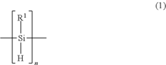
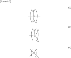
Polysilane and polysilane-containing resin composition
PatentInactiveUS8163863B2
Innovation
- Introducing a Si—H group into the polysilane main chain and bonding a hydrosilylatable compound with functional groups like hydroxyl, carboxyl, or epoxy groups, allowing for controlled hydrosilylation to enhance solubility and reactivity without complex steps or special apparatus.


Semiconductor device having gate electrode connection to wiring layer
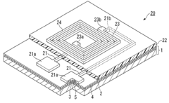
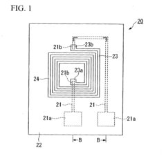
PatentInactiveUS20080203527A1
Innovation
- A semiconductor device design featuring a first and second insulating resin layer with specific thicknesses and openings, along with a first and second wiring layer, where the second wiring layer includes an induction element, such as a spiral coil, spaced apart from the semiconductor substrate to minimize energy loss and maximize the quality factor.
Environmental Impact
The adoption of polysilane in semiconductor devices not only enhances energy efficiency but also contributes significantly to reducing the environmental impact of the electronics industry. As energy loss in semiconductor devices decreases, the overall power consumption of electronic systems diminishes, leading to a cascade of positive environmental effects.
Primarily, the reduction in energy loss translates to lower electricity demand for operating electronic devices. This decreased energy requirement has far-reaching implications for power generation and distribution systems. Power plants can potentially scale back their output, resulting in reduced fossil fuel consumption and, consequently, lower greenhouse gas emissions. The cumulative effect of widespread polysilane adoption could contribute to mitigating climate change and improving air quality on a global scale.
Furthermore, the improved energy efficiency of semiconductor devices extends the battery life of portable electronics. This extension has a dual environmental benefit. Firstly, it reduces the frequency of battery charging, further decreasing electricity consumption. Secondly, it potentially slows down the rate of battery replacements, thereby reducing electronic waste generation. The production and disposal of batteries are associated with significant environmental concerns, including toxic material leaching and resource depletion.
The manufacturing process of polysilane-based semiconductors also presents opportunities for environmental improvement. Compared to traditional semiconductor materials, polysilane can be synthesized using less energy-intensive methods. This reduction in manufacturing energy requirements further decreases the carbon footprint associated with semiconductor production. Additionally, polysilane's potential for solution-based processing could lead to more environmentally friendly manufacturing techniques, reducing the use of harsh chemicals and minimizing waste generation.
In the context of the growing Internet of Things (IoT) and the proliferation of electronic devices, the environmental impact of polysilane becomes even more significant. As billions of devices are connected and integrated into various aspects of daily life, the cumulative energy savings from polysilane-enhanced semiconductors could be substantial. This efficiency gain is particularly crucial in data centers and cloud computing infrastructure, where energy consumption is a major environmental concern.
Lastly, the adoption of polysilane in semiconductor devices aligns with global sustainability goals and regulatory trends. As governments and organizations worldwide push for more stringent energy efficiency standards, polysilane technology positions the electronics industry to meet and exceed these requirements. This proactive approach not only ensures compliance but also drives innovation towards more sustainable electronic products, fostering a circular economy in the tech sector.
Manufacturing Scalability
The manufacturing scalability of polysilane-based semiconductor devices presents both opportunities and challenges for the industry. As the demand for more energy-efficient electronic components grows, the ability to produce polysilane-enhanced devices at scale becomes crucial. Current manufacturing processes for traditional semiconductor devices can be adapted to incorporate polysilane materials, but several factors need to be considered to ensure successful large-scale production.
One of the primary considerations is the integration of polysilane synthesis into existing semiconductor fabrication lines. Polysilane can be synthesized through various methods, including electrochemical reduction, catalytic dehydrocoupling, and Wurtz-type coupling reactions. Each method has its own set of requirements in terms of equipment, precursors, and process conditions. Manufacturers must evaluate which synthesis method aligns best with their current infrastructure and can be scaled up most efficiently.
The deposition of polysilane onto semiconductor substrates is another critical aspect of manufacturing scalability. Techniques such as chemical vapor deposition (CVD), spin-coating, and plasma-enhanced CVD have shown promise for large-scale application of polysilane films. However, achieving uniform thickness and consistent material properties across large wafer sizes remains a challenge that requires further optimization.
Quality control and characterization of polysilane-enhanced devices at scale pose additional challenges. Developing robust in-line monitoring techniques to ensure the consistency of polysilane properties throughout the manufacturing process is essential. This may involve the adaptation of existing metrology tools or the development of new ones specifically tailored for polysilane materials.
Environmental considerations also play a role in scaling up polysilane production. Some synthesis methods may involve the use of hazardous materials or generate byproducts that require careful handling and disposal. Manufacturers must implement appropriate safety measures and waste management systems to comply with regulations and maintain sustainable production practices.
The supply chain for polysilane precursors and related materials is another factor that impacts manufacturing scalability. Ensuring a stable and cost-effective supply of high-purity precursors is crucial for maintaining consistent production volumes. Collaboration with chemical suppliers and potentially developing in-house synthesis capabilities may be necessary to meet the demands of large-scale manufacturing.
As the technology matures, automation and process optimization will become increasingly important for improving yield and reducing production costs. This may involve the development of specialized equipment for polysilane handling and integration, as well as the implementation of advanced process control systems to fine-tune manufacturing parameters.
In conclusion, while challenges exist, the potential benefits of polysilane in reducing energy loss in semiconductor devices make overcoming these manufacturing hurdles a worthwhile endeavor. As research progresses and industry adoption grows, it is likely that more efficient and scalable manufacturing solutions will emerge, paving the way for widespread implementation of this promising technology.
Unlock deeper insights with Patsnap Eureka Quick Research — get a full tech report to explore trends and direct your research. Try now!
Generate Your Research Report Instantly with AI Agent
Supercharge your innovation with Patsnap Eureka AI Agent Platform!