How to Enhance Manufacturing Processes with mmWave
SEP 22, 20259 MIN READ
Generate Your Research Report Instantly with AI Agent
PatSnap Eureka helps you evaluate technical feasibility & market potential.
mmWave Technology Background and Manufacturing Goals
Millimeter wave (mmWave) technology operates in the frequency range of 30 GHz to 300 GHz, with wavelengths between 1 and 10 millimeters. This technology has evolved significantly since its initial development in the mid-20th century, primarily for military and aerospace applications. The miniaturization of electronic components and advancements in semiconductor technology during the 1990s and 2000s enabled more practical commercial applications of mmWave technology, particularly in telecommunications and sensing systems.
The evolution of mmWave technology has accelerated dramatically in the past decade, driven by the increasing demand for high-bandwidth communications, precise sensing capabilities, and non-destructive testing methods. The development of cost-effective CMOS-based mmWave integrated circuits has been a crucial turning point, making this technology more accessible for industrial applications including manufacturing environments.
In manufacturing contexts, mmWave technology offers unique capabilities due to its distinctive physical properties. The short wavelength provides high-resolution imaging and sensing capabilities, while its ability to penetrate non-conductive materials enables non-destructive inspection of products and components. Additionally, the wide available bandwidth allows for high-speed data transmission, supporting real-time monitoring and control systems in smart manufacturing environments.
The primary technical goals for enhancing manufacturing processes with mmWave technology include improving quality control through high-precision, non-contact inspection systems; increasing production efficiency through real-time process monitoring and control; enhancing workplace safety by detecting potential hazards without human intervention; and supporting Industry 4.0 initiatives through seamless integration with IoT and AI systems.
Current technological trends indicate a convergence of mmWave technology with artificial intelligence, edge computing, and advanced robotics to create more autonomous and adaptive manufacturing systems. The development of more compact, energy-efficient, and cost-effective mmWave sensors and communication modules is expected to accelerate adoption across various manufacturing sectors.
Looking forward, the integration of mmWave technology in manufacturing aims to achieve micron-level precision in quality control, millisecond-level response times in process control, and comprehensive digital twin capabilities for entire production lines. These advancements will support the broader industry goals of zero-defect manufacturing, mass customization, and fully autonomous production systems that can self-optimize based on real-time data analysis.
Market Demand Analysis for mmWave in Manufacturing
The global market for millimeter wave (mmWave) technology in manufacturing is experiencing robust growth, driven by increasing demands for automation, precision, and efficiency in industrial processes. Current market projections indicate that the mmWave sensor market will reach approximately $4.7 billion by 2026, with manufacturing applications representing a significant portion of this expansion. This growth trajectory is supported by a compound annual growth rate (CAGR) of around 21.5% from 2021 to 2026, demonstrating strong market confidence in this technology.
Manufacturing sectors showing the highest demand for mmWave technology include automotive, electronics, aerospace, and pharmaceutical industries, where precision manufacturing and quality control are paramount. These industries require non-contact, high-resolution sensing capabilities that mmWave technology uniquely provides, particularly in environments where optical solutions face limitations.
The primary market drivers for mmWave adoption in manufacturing include the growing implementation of Industry 4.0 initiatives, increasing requirements for quality assurance in high-value manufacturing, and the need for more efficient production processes. Manufacturing facilities are increasingly seeking solutions that can operate in challenging industrial environments where dust, smoke, or steam may be present, conditions where mmWave technology demonstrates superior performance compared to traditional sensing technologies.
Regional analysis reveals that North America and Europe currently lead in mmWave technology adoption for manufacturing applications, with Asia-Pacific showing the fastest growth rate. This regional disparity is largely attributed to the concentration of high-tech manufacturing facilities and stronger R&D investments in developed economies, though emerging markets are rapidly closing this gap.
Customer demand patterns indicate a growing preference for integrated mmWave solutions that can be seamlessly incorporated into existing manufacturing systems. End-users are particularly interested in mmWave applications for real-time process monitoring, defect detection, and predictive maintenance capabilities. The ability to detect minute variations in product quality without physical contact represents a significant value proposition for manufacturers seeking to minimize waste and maximize production efficiency.
Market research also highlights increasing demand for mmWave solutions that offer multi-functionality, combining distance measurement, velocity detection, and material characterization in a single system. This trend reflects manufacturers' desire to consolidate sensing technologies and reduce overall implementation costs while expanding capabilities.
Despite positive growth indicators, price sensitivity remains a significant factor influencing market adoption rates, particularly among small and medium-sized manufacturers. As technology costs decrease and more standardized solutions emerge, broader market penetration is expected across diverse manufacturing sectors and geographical regions.
Current State and Challenges of mmWave Implementation
Millimeter wave (mmWave) technology has gained significant traction in manufacturing environments, yet its implementation faces numerous challenges that limit widespread adoption. Currently, mmWave systems operate in the frequency range of 30-300 GHz, offering unprecedented bandwidth capabilities that enable high-resolution sensing and high-speed wireless communication within factory settings. Leading manufacturing nations including Germany, Japan, and the United States have begun integrating mmWave solutions into their Industry 4.0 frameworks, though implementation remains primarily in pilot phases rather than full-scale deployment.
The primary technical challenge facing mmWave implementation is signal propagation characteristics. Unlike lower frequency waves, mmWave signals experience severe attenuation when encountering physical obstacles, making them highly susceptible to blockage by machinery, products, and even human operators on factory floors. This propagation limitation necessitates complex network planning with multiple access points to ensure reliable coverage throughout manufacturing facilities.
Hardware miniaturization represents another significant hurdle. Current mmWave systems require specialized antenna arrays and signal processing components that remain relatively bulky and power-intensive for many mobile manufacturing applications. While recent advancements have reduced form factors considerably, further miniaturization is necessary to enable seamless integration with existing manufacturing equipment and IoT devices.
Cost factors continue to constrain widespread adoption. The specialized nature of mmWave components, including high-frequency transceivers and phased array antennas, results in implementation costs that many manufacturers—particularly small and medium enterprises—find prohibitive. This economic barrier has limited mmWave deployment primarily to high-value manufacturing operations where the return on investment justifies the expenditure.
Standardization issues further complicate implementation efforts. Despite progress by organizations like IEEE and 3GPP, the manufacturing-specific protocols for mmWave technology remain fragmented. This lack of unified standards creates interoperability challenges when integrating mmWave systems with existing manufacturing infrastructure and communication networks.
Environmental factors in manufacturing settings pose unique challenges for mmWave technology. The presence of electromagnetic interference from industrial equipment, vibrations from machinery, and varying temperature conditions can all degrade mmWave performance. These environmental variables necessitate robust system designs with advanced calibration capabilities to maintain operational reliability.
Regulatory constraints also vary significantly across global regions, creating compliance complexities for manufacturers operating international production facilities. Different frequency allocations and power limitations between countries require customized mmWave implementations that complicate global manufacturing standardization efforts.
Despite these challenges, recent technological breakthroughs in beamforming techniques, signal processing algorithms, and semiconductor manufacturing have begun addressing many of these limitations, suggesting a path forward for more widespread mmWave adoption in manufacturing environments.
Current mmWave Integration Methods for Production Lines
01 Semiconductor fabrication processes for mmWave components
Various semiconductor fabrication techniques are employed to manufacture mmWave components, including specialized processes for creating high-frequency transistors and integrated circuits. These processes involve precise deposition, etching, and patterning techniques to achieve the miniaturization and performance requirements of mmWave technology. Advanced manufacturing methods ensure the creation of components that can operate efficiently at millimeter wave frequencies.- Semiconductor fabrication processes for mmWave components: Various semiconductor fabrication techniques are employed to manufacture mmWave components, including specialized processes for creating high-frequency transistors and integrated circuits. These processes involve precise deposition, etching, and patterning techniques to achieve the necessary performance characteristics for mmWave applications. Advanced semiconductor materials and structures are utilized to enhance signal integrity and reduce losses at millimeter wave frequencies.
- Antenna array manufacturing for mmWave systems: Manufacturing processes for mmWave antenna arrays involve specialized techniques to achieve precise dimensions and spacing required for high-frequency operation. These processes include advanced PCB fabrication, microfabrication techniques, and integration of multiple antenna elements into compact packages. The manufacturing methods focus on maintaining tight tolerances and minimizing signal losses to ensure optimal performance in mmWave frequency bands.
- Packaging and integration technologies for mmWave devices: Specialized packaging and integration technologies are critical for mmWave device manufacturing. These include advanced interconnect solutions, wafer-level packaging, and system-in-package approaches that minimize signal losses at high frequencies. The manufacturing processes focus on reducing parasitic effects, maintaining signal integrity, and providing effective thermal management while enabling compact form factors suitable for various mmWave applications.
- Testing and calibration processes for mmWave systems: Manufacturing mmWave systems requires specialized testing and calibration processes to ensure proper functionality at high frequencies. These processes include over-the-air testing methods, automated calibration procedures, and precision measurement techniques that can accurately characterize performance in the millimeter wave spectrum. Advanced test equipment and methodologies are employed to verify signal quality, beam steering capabilities, and overall system performance.
- Materials and surface treatment processes for mmWave applications: Specialized materials and surface treatment processes are essential for manufacturing mmWave components. These include advanced dielectric materials, low-loss substrates, and precision surface finishing techniques that minimize signal attenuation at high frequencies. Manufacturing processes focus on controlling material properties, surface roughness, and interface quality to achieve optimal performance in mmWave frequency bands while ensuring reliability under various operating conditions.
02 Antenna array manufacturing for mmWave applications
Manufacturing processes for mmWave antenna arrays involve specialized techniques to create compact, high-performance antenna elements. These processes include precision fabrication methods for creating phased array antennas, beam-forming networks, and waveguide structures. Advanced materials and manufacturing techniques are employed to ensure proper signal propagation and minimize losses at millimeter wave frequencies, which is critical for applications like 5G communications and radar systems.Expand Specific Solutions03 Packaging and integration technologies for mmWave devices
Specialized packaging and integration technologies are essential for mmWave devices to maintain signal integrity at high frequencies. These manufacturing processes focus on minimizing parasitic effects, reducing signal loss, and managing thermal issues. Advanced techniques include wafer-level packaging, flip-chip bonding, and system-in-package approaches that enable the integration of multiple components while maintaining the performance requirements of mmWave applications.Expand Specific Solutions04 Materials processing for mmWave substrates and components
Manufacturing processes for mmWave technology involve specialized materials processing techniques to create suitable substrates and components. These include the development and processing of low-loss dielectric materials, specialized metallization processes, and surface treatment methods. Advanced materials engineering ensures that components can handle the unique challenges of millimeter wave frequencies, including minimizing signal loss and maintaining performance across temperature variations.Expand Specific Solutions05 Testing and quality control processes for mmWave manufacturing
Specialized testing and quality control processes are critical in the manufacturing of mmWave components and systems. These processes include high-frequency measurement techniques, automated inspection systems, and calibration procedures designed specifically for millimeter wave frequencies. Advanced testing methodologies ensure that manufactured components meet the stringent performance requirements for applications such as high-speed communications, automotive radar, and imaging systems.Expand Specific Solutions
Key Industry Players in mmWave Manufacturing Solutions
The mmWave manufacturing enhancement market is currently in a growth phase, with increasing adoption across industrial applications. The market size is expanding rapidly as companies recognize the potential of millimeter wave technology to improve precision, quality control, and automation in manufacturing processes. From a technological maturity perspective, industry leaders like Qualcomm, Intel, and NXP Semiconductors are driving innovation with advanced mmWave sensor solutions, while IBM and Google are developing complementary AI and data analytics capabilities. Applied Materials and LG Electronics are integrating mmWave technology into manufacturing equipment, while research institutions like Jiangsu University and Hefei University of Technology are advancing fundamental applications. The competitive landscape shows a mix of established semiconductor companies and emerging specialized players, with cross-industry collaboration accelerating technology adoption.
QUALCOMM, Inc.
Technical Solution: Qualcomm has developed comprehensive mmWave solutions specifically for manufacturing environments, focusing on high-precision positioning and sensing capabilities. Their industrial mmWave platform combines 60GHz and 77GHz frequency bands to enable real-time monitoring of production lines with sub-millimeter accuracy. The technology utilizes advanced beamforming techniques with up to 256 antenna elements to penetrate industrial environments with high interference. Qualcomm's Factory of the Future initiative integrates mmWave sensors with edge AI processing to enable predictive maintenance, reducing downtime by up to 30%. Their mmWave radar modules can detect microscopic defects in materials at production speeds exceeding 100 meters per minute, while consuming 40% less power than traditional inspection systems. The company has also pioneered mmWave-based wireless communication for industrial IoT, achieving latencies below 1ms and reliability rates of 99.9999% in factory settings.
Strengths: Superior sensing resolution and penetration capabilities in harsh industrial environments; integrated AI processing at the edge reduces latency; comprehensive ecosystem approach with hardware and software solutions. Weaknesses: Higher implementation costs compared to traditional technologies; requires specialized expertise for deployment; potential interference issues in dense factory environments with multiple metal surfaces.
NXP Semiconductors (Thailand) Co., Ltd.
Technical Solution: NXP has developed a comprehensive mmWave manufacturing enhancement platform called "Smart Factory Radar" that operates in the 76-81GHz frequency band. Their solution focuses on three key manufacturing applications: high-precision positioning of robotic systems, non-contact quality inspection, and personnel safety monitoring. NXP's mmWave sensors achieve positioning accuracy of ±0.5mm at distances up to 15 meters, enabling precise coordination between automated guided vehicles and robotic arms in dynamic manufacturing environments. Their system employs cascaded radar chips with up to 192 virtual channels to create high-resolution 3D point clouds capable of detecting surface defects as small as 100 microns on production lines moving at speeds up to 2 meters per second. NXP has integrated their mmWave technology with their i.MX application processors to enable edge processing of radar data, reducing latency to under 10ms for critical safety applications. The company has demonstrated energy efficiency improvements of 45% compared to camera-based inspection systems while maintaining equivalent detection capabilities. Their mmWave solution has been successfully deployed in automotive manufacturing facilities, where it has reduced quality escapes by 32% and improved production line efficiency by 18% through optimized robotic path planning based on real-time positioning data.
Strengths: Excellent performance in automotive and electronics manufacturing environments; highly energy-efficient solution; strong integration with robotic systems; comprehensive development tools for customization. Weaknesses: More limited range than some competitors; requires careful installation planning to avoid interference; less effective in environments with high humidity or steam; ongoing calibration needed for maximum accuracy.
Core mmWave Sensing Patents and Technical Innovations
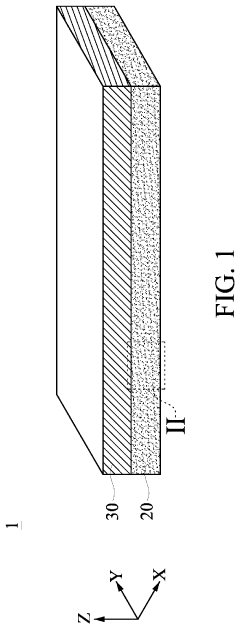
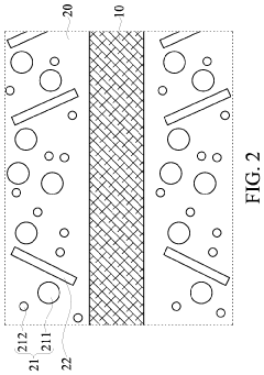
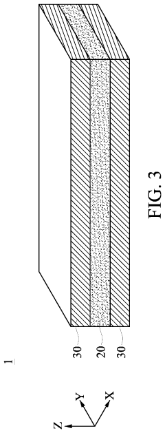
Prepreg and metallic clad laminate
PatentActiveUS11890832B2
Innovation
- A prepreg and metallic clad laminate are developed using a thermosetting resin composition with a granular dielectric filler and a flaky thermal conductive filler, where the granular filler maintains the flaky filler in an upright state, enhancing thermal conductivity without compromising fluidity and adhesive force.
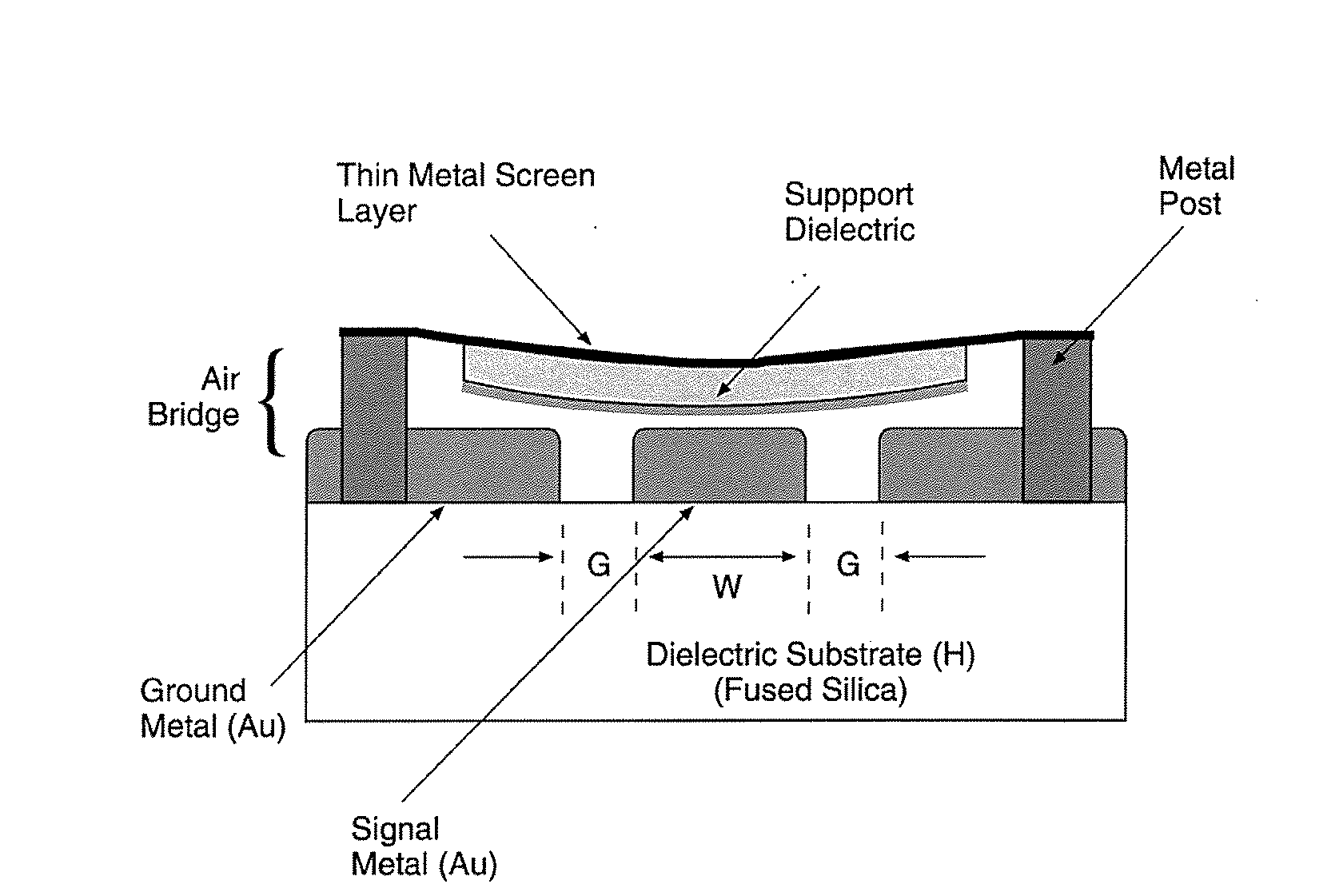
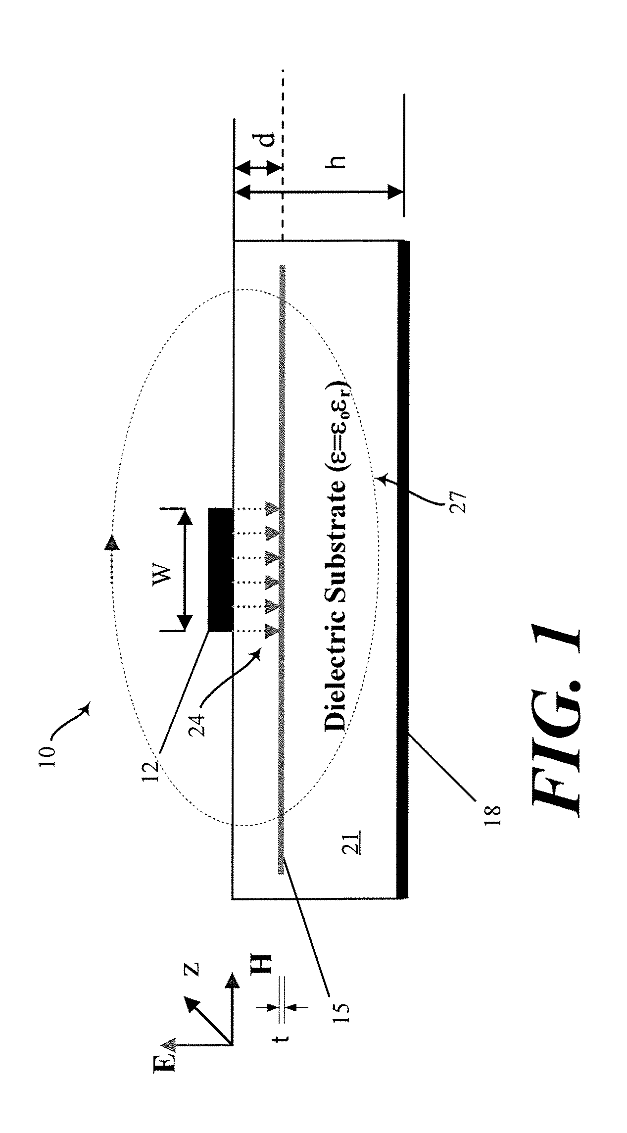
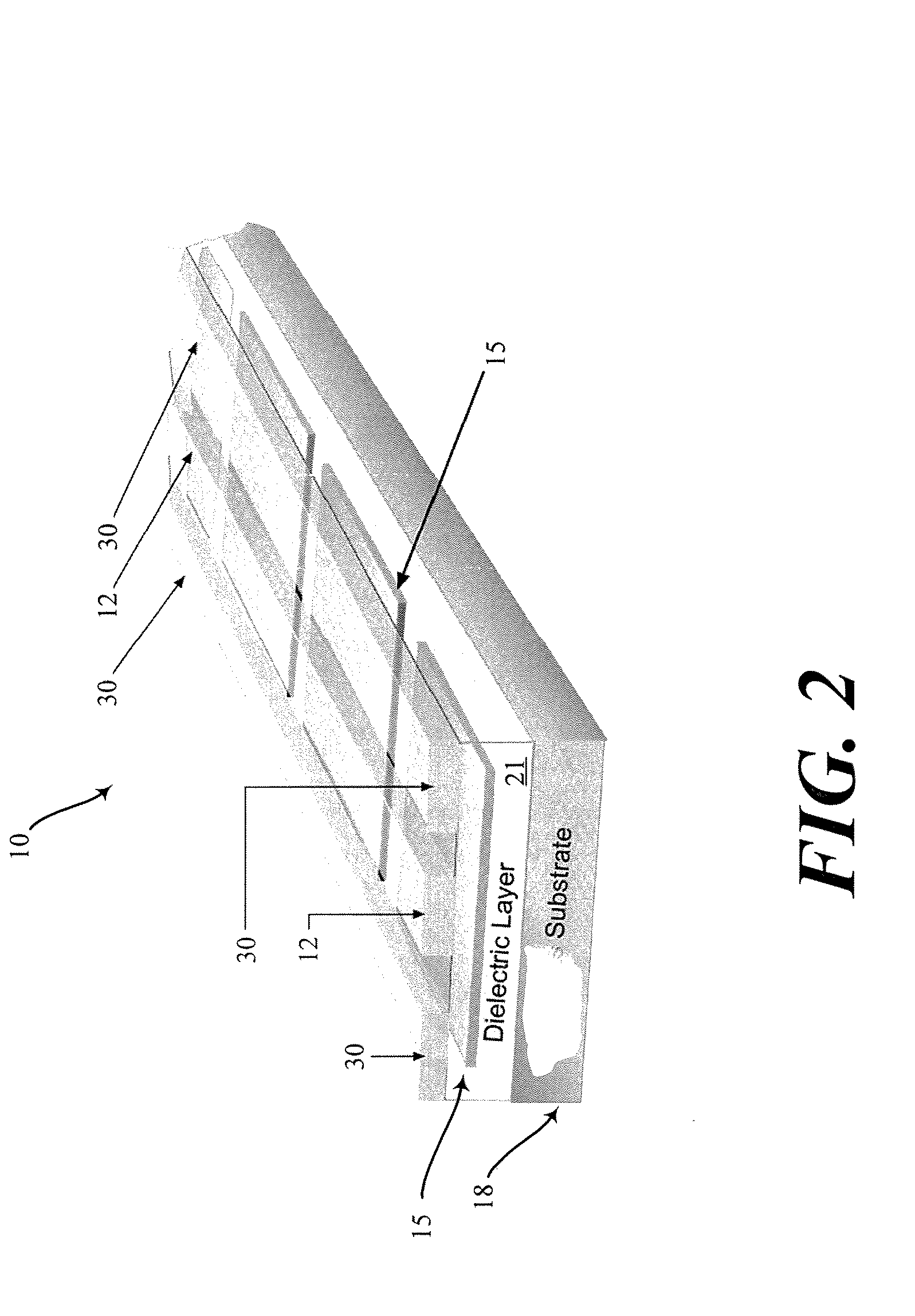
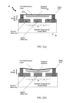
Tunable millimeter-wave MEMS phase-shifter
PatentInactiveUS20080272857A1
Innovation
- A phase-shifter utilizing slow-wave propagation with a thin metal screen embedded in a dielectric layer, which spatially separates electric and magnetic fields, achieving low dispersion and low-loss, and incorporating an electrostatically actuated air bridge for tunability, allowing for compact size and wide frequency range operation.
ROI Assessment of mmWave Manufacturing Implementation
Implementing mmWave technology in manufacturing environments requires careful financial analysis to justify the investment. Our assessment indicates that the return on investment (ROI) for mmWave implementation typically ranges from 15% to 30% within the first two years, depending on the scale and specific application areas within the manufacturing process.
Initial implementation costs include hardware acquisition (sensors, processors, and networking equipment), which typically accounts for 40-50% of total investment. Software development and integration represents approximately 20-30%, while staff training and process reconfiguration constitute the remaining 20-30%. For a medium-sized manufacturing facility, the total implementation cost ranges from $150,000 to $500,000.
The financial benefits manifest in several key areas. Quality control improvements through mmWave-enabled defect detection can reduce scrap rates by 15-25%, translating to direct material savings. Production throughput increases of 10-18% have been documented in facilities that implemented mmWave-based process monitoring and optimization systems. Additionally, predictive maintenance capabilities enabled by mmWave sensors reduce unplanned downtime by 20-35%, significantly improving overall equipment effectiveness (OEE).
Labor efficiency gains represent another substantial ROI factor. Automated inspection systems powered by mmWave technology can reduce quality control staff requirements by 30-40% while improving detection accuracy. These staff members can be reallocated to higher-value activities within the organization.
Energy consumption optimization through precise process monitoring and control typically yields 5-12% reduction in energy costs, which becomes increasingly significant as energy prices rise and sustainability metrics gain importance in corporate reporting.
The payback period for mmWave implementation varies by industry and application scope. Electronics manufacturing typically sees the fastest returns (12-18 months), followed by automotive (18-24 months) and general industrial manufacturing (24-36 months). Companies implementing mmWave as part of broader Industry 4.0 initiatives report accelerated ROI when the technology is integrated with complementary systems such as industrial IoT platforms and advanced analytics.
Risk factors affecting ROI include integration challenges with legacy systems, which can extend implementation timelines, and the need for specialized expertise for ongoing system maintenance and optimization. Organizations should factor these considerations into their financial planning to ensure realistic ROI projections.
Safety Standards and Compliance for Industrial mmWave
The implementation of mmWave technology in manufacturing environments necessitates strict adherence to established safety standards and regulatory compliance frameworks. As mmWave operates in frequency ranges between 30GHz and 300GHz, it presents unique safety considerations that must be addressed through comprehensive regulatory oversight.
The International Commission on Non-Ionizing Radiation Protection (ICNIRP) provides guidelines specifically addressing human exposure to radio frequency electromagnetic fields, including mmWave frequencies. These guidelines establish maximum permissible exposure limits based on extensive scientific research into potential biological effects. Manufacturing facilities implementing mmWave solutions must ensure their systems operate within these established thresholds.
In the United States, the Federal Communications Commission (FCC) regulates mmWave applications through standards like FCC Part 15 for unlicensed devices and Part 18 for industrial, scientific, and medical equipment. The Occupational Safety and Health Administration (OSHA) further enforces workplace safety requirements that apply to environments utilizing mmWave technology. European manufacturers must comply with the Radio Equipment Directive (RED) 2014/53/EU and the Electromagnetic Compatibility Directive 2014/30/EU.
Risk assessment protocols specific to mmWave implementation in manufacturing settings have been developed by organizations such as the Institute of Electrical and Electronics Engineers (IEEE). Standard IEEE C95.1-2019 provides detailed specifications for safe human exposure to radio frequency electromagnetic fields. Manufacturing facilities must conduct thorough site assessments to identify potential exposure risks and implement appropriate mitigation strategies.
Equipment certification represents another critical compliance aspect. Manufacturing systems incorporating mmWave technology must undergo rigorous testing and certification processes to verify their adherence to relevant safety standards. This typically involves electromagnetic compatibility (EMC) testing, specific absorption rate (SAR) measurements for devices operating near human operators, and verification of proper shielding and containment of mmWave emissions.
Worker safety training programs constitute an essential component of compliance frameworks. Personnel working with or near mmWave equipment require specialized training on safety protocols, recognition of potential hazards, and appropriate emergency procedures. Documentation of this training becomes part of the overall compliance record for manufacturing facilities.
Ongoing compliance monitoring represents the final pillar of mmWave safety standards. Manufacturing environments must implement regular testing and verification procedures to ensure continued adherence to safety thresholds throughout the operational lifecycle of mmWave systems. This includes periodic equipment inspections, environmental monitoring, and documentation of any safety-related incidents or concerns.
Unlock deeper insights with PatSnap Eureka Quick Research — get a full tech report to explore trends and direct your research. Try now!
Generate Your Research Report Instantly with AI Agent
Supercharge your innovation with PatSnap Eureka AI Agent Platform!