How to Explore Polysilane's Photonic Properties?
JUL 11, 20259 MIN READ
Generate Your Research Report Instantly with AI Agent
Patsnap Eureka helps you evaluate technical feasibility & market potential.
Polysilane Photonics Background and Objectives
Polysilanes, a class of silicon-based polymers, have garnered significant attention in the field of photonics due to their unique electronic and optical properties. The exploration of polysilane's photonic properties has been an ongoing endeavor since the 1980s, with researchers continuously uncovering new potential applications in various technological domains.
The primary objective in exploring polysilane's photonic properties is to harness their exceptional characteristics for advanced optical and electronic applications. These materials exhibit strong σ-conjugation along the silicon backbone, leading to interesting photophysical phenomena such as UV absorption, photoconductivity, and photoluminescence. Understanding and manipulating these properties could pave the way for novel optoelectronic devices, sensors, and photonic materials.
One of the key goals in this field is to develop polysilanes with tailored optical properties for specific applications. This involves synthesizing new polysilane structures, investigating their structure-property relationships, and optimizing their performance in various photonic systems. Researchers aim to enhance the quantum yield of photoluminescence, improve charge carrier mobility, and expand the range of accessible wavelengths for light emission and absorption.
Another crucial objective is to explore the potential of polysilanes in emerging technologies such as organic electronics, photovoltaics, and optical data storage. The unique combination of silicon-based chemistry and polymeric properties offers exciting possibilities for creating hybrid materials that bridge the gap between traditional inorganic semiconductors and organic polymers.
The evolution of polysilane photonics has been marked by several significant milestones. Early research focused on understanding the fundamental photophysics of these materials, including their electronic structure and excited-state dynamics. Subsequent developments led to the synthesis of various polysilane architectures, including linear, cyclic, and branched structures, each with distinct optical properties.
Recent trends in polysilane photonics research include the exploration of nanostructured polysilanes, such as nanoparticles and thin films, which exhibit enhanced optical properties due to quantum confinement effects. Additionally, there is growing interest in incorporating polysilanes into composite materials and hybrid systems to create multifunctional photonic devices.
As the field progresses, researchers are increasingly focusing on practical applications of polysilane photonics. This includes the development of efficient blue light-emitting diodes, UV-sensitive photoresists for lithography, and high-performance photovoltaic cells. The potential for polysilanes in next-generation display technologies and optical computing is also being actively investigated.
Market Potential for Polysilane-based Photonic Devices
The market potential for polysilane-based photonic devices is significant and growing, driven by the increasing demand for advanced optical and electronic components across various industries. Polysilanes, with their unique photonic properties, offer promising applications in areas such as optoelectronics, photovoltaics, and sensing technologies.
In the optoelectronics sector, polysilane-based devices show potential for use in light-emitting diodes (LEDs), organic light-emitting diodes (OLEDs), and electroluminescent displays. The tunable optical properties of polysilanes allow for the development of devices with customizable emission wavelengths, potentially leading to more efficient and versatile display technologies.
The photovoltaic industry represents another significant market opportunity for polysilane-based devices. As the world shifts towards renewable energy sources, there is a growing demand for more efficient and cost-effective solar cells. Polysilanes' unique electronic properties and potential for solution processing make them attractive candidates for next-generation solar cell technologies, potentially offering improved efficiency and reduced manufacturing costs.
Sensing technologies also present a promising market for polysilane-based devices. The photosensitive nature of polysilanes makes them suitable for applications in chemical and biological sensors, as well as in environmental monitoring systems. These sensors could find use in industries such as healthcare, environmental protection, and industrial process control.
The telecommunications industry is another potential market for polysilane-based photonic devices. With the increasing demand for high-speed data transmission, there is a need for advanced optical components in fiber-optic networks. Polysilane-based devices could potentially be used in optical switches, modulators, and other components to enhance the performance of telecommunications infrastructure.
In the field of data storage, polysilanes show promise for use in optical data storage devices. Their photochromic properties could enable the development of high-density, rewritable optical storage media with improved performance compared to current technologies.
While the market potential for polysilane-based photonic devices is substantial, it is important to note that the technology is still in its early stages of development. Significant research and development efforts are required to overcome current limitations and bring these devices to commercial viability. However, as the technology matures and manufacturing processes improve, the market for polysilane-based photonic devices is expected to expand rapidly across multiple industries.
Current Challenges in Polysilane Photonics Research
The exploration of polysilane's photonic properties faces several significant challenges that hinder progress in this promising field. One of the primary obstacles is the complexity of synthesizing high-quality polysilane materials with consistent molecular weights and controlled structures. The photonic properties of polysilanes are highly dependent on their molecular architecture, and achieving precise control over these structures remains a formidable task.
Another major challenge lies in the stability of polysilane materials under various environmental conditions. Many polysilanes are sensitive to light, heat, and oxygen, which can lead to degradation and alteration of their photonic properties over time. This instability poses difficulties in both research settings and potential practical applications, necessitating the development of more robust polysilane derivatives or effective encapsulation techniques.
The characterization of polysilane photonic properties presents its own set of challenges. Advanced spectroscopic techniques are required to fully understand the complex photophysics of these materials, including their excited-state dynamics and energy transfer processes. The need for specialized equipment and expertise in interpreting the results can limit the accessibility of polysilane research to many laboratories.
Furthermore, the integration of polysilanes into functional photonic devices remains a significant hurdle. While the unique optical properties of polysilanes make them attractive for various applications, such as light-emitting diodes or photovoltaic cells, translating these properties into efficient and reliable devices is not straightforward. Issues such as interfacial compatibility, charge transport, and long-term performance stability need to be addressed.
The theoretical understanding of polysilane photonics also lags behind experimental observations in some areas. Developing accurate models to predict and explain the photonic behavior of complex polysilane systems is crucial for guiding experimental work and accelerating progress in the field. This requires interdisciplinary collaboration between synthetic chemists, physicists, and computational scientists.
Lastly, the scalability of polysilane synthesis and device fabrication processes poses a challenge for potential commercial applications. Current methods often yield small quantities of materials or are not easily adaptable to large-scale production. Overcoming these scaling issues is essential for the practical implementation of polysilane-based photonic technologies.
Existing Methods for Exploring Polysilane Photonic Properties
01 Optical and electronic properties of polysilanes
Polysilanes exhibit unique optical and electronic properties due to their σ-conjugated backbone structure. These properties include photoconductivity, electroluminescence, and nonlinear optical effects. The delocalization of electrons along the silicon backbone contributes to their photonic characteristics, making them suitable for various optoelectronic applications.- Optical and electronic properties of polysilanes: Polysilanes exhibit unique optical and electronic properties due to their σ-conjugated backbone structure. These properties include photoconductivity, electroluminescence, and nonlinear optical effects. The delocalization of electrons along the silicon backbone contributes to their photonic characteristics, making them suitable for various optoelectronic applications.
- Polysilane-based photonic devices: Polysilanes can be used to fabricate various photonic devices such as light-emitting diodes, photodetectors, and optical waveguides. Their tunable optical properties and processability make them attractive for integrated photonic circuits and optoelectronic applications. These materials can be engineered to manipulate light at the nanoscale, enabling novel photonic functionalities.
- Synthesis and modification of polysilanes for enhanced photonic properties: Various synthesis methods and modification techniques are employed to enhance the photonic properties of polysilanes. These include the incorporation of functional side groups, copolymerization with other silicon-containing monomers, and the formation of nanostructured materials. Such modifications can lead to improved light emission, absorption, and charge transport characteristics.
- Photosensitivity and photopatterning of polysilanes: Polysilanes exhibit photosensitivity, allowing for their use in photolithography and photopatterning applications. Upon exposure to UV light, polysilanes can undergo photochemical reactions, leading to changes in their molecular structure and properties. This characteristic enables the creation of micro- and nanostructures for photonic applications.
- Integration of polysilanes in hybrid photonic materials: Polysilanes can be combined with other materials to create hybrid photonic structures with enhanced properties. These hybrid materials may include inorganic nanoparticles, organic dyes, or other polymers. The resulting composites can exhibit improved light emission, energy transfer, or nonlinear optical properties, expanding their potential in advanced photonic applications.
02 Polysilane-based photonic devices
Polysilanes can be used to fabricate various photonic devices such as light-emitting diodes, photovoltaic cells, and optical waveguides. Their tunable optical properties and processability make them attractive materials for integrated photonic circuits and optoelectronic components.Expand Specific Solutions03 Synthesis and modification of polysilanes for enhanced photonic properties
Various synthesis methods and chemical modifications can be employed to enhance the photonic properties of polysilanes. These include the incorporation of functional side groups, copolymerization with other silicon-containing monomers, and the formation of nanostructured materials to optimize their optical characteristics.Expand Specific Solutions04 Photosensitivity and photopatterning of polysilanes
Polysilanes exhibit photosensitivity, allowing for their use in photolithography and photopatterning applications. Upon exposure to UV light, they undergo photochemical reactions that can alter their solubility or chemical structure, enabling the creation of micro- and nanostructures for photonic devices.Expand Specific Solutions05 Polysilane-based photonic crystals and metamaterials
Polysilanes can be used to create photonic crystals and metamaterials with unique light-manipulating properties. These structures can exhibit photonic bandgaps, negative refractive indices, or other exotic optical phenomena, opening up possibilities for advanced photonic applications such as optical computing and sensing.Expand Specific Solutions
Key Players in Polysilane and Photonics Research
The exploration of polysilane's photonic properties is in an early developmental stage, with the market still emerging and relatively small. The technology's maturity is low, indicating significant potential for growth and innovation. Key players like JSR Corp., Dow Silicones Corp., and Nippon Paint Co., Ltd. are actively researching and developing applications in this field. These companies are leveraging their expertise in materials science and chemical engineering to advance polysilane technology. The competitive landscape is characterized by a mix of established chemical companies and specialized research institutions, suggesting a collaborative approach to overcoming technical challenges and expanding potential applications in photonics and optoelectronics.
Merck Patent GmbH
Technical Solution: Merck Patent GmbH has been actively exploring polysilane's photonic properties with a focus on industrial applications. Their research strategy involves developing scalable synthesis methods for high-performance polysilanes suitable for optoelectronic devices[1]. They have patented several novel polysilane derivatives with improved thermal stability and photoluminescence quantum yields, making them ideal for use in display technologies[2]. Merck has also investigated the incorporation of polysilanes into photovoltaic cells as light-harvesting materials, exploiting their broad absorption spectra and efficient charge transport properties[3]. Furthermore, they have developed polysilane-based photoresists for next-generation lithography processes, leveraging the material's high sensitivity to UV and electron beam exposure[4].
Strengths: Strong focus on practical applications, extensive patent portfolio, and capability for large-scale production. Weaknesses: Potential limitations in exploring more fundamental aspects of polysilane photophysics due to commercial focus.
Japan Science & Technology Agency
Technical Solution: The Japan Science & Technology Agency (JST) has been supporting and coordinating research efforts to explore polysilane's photonic properties across various institutions in Japan. Their approach involves a multidisciplinary strategy, combining expertise from chemistry, physics, and materials science[1]. JST-funded projects have focused on developing new synthetic routes for functional polysilanes with enhanced photonic properties, such as two-photon absorption and nonlinear optical responses[2]. They have also supported research into the fundamental photophysics of polysilanes, including ultrafast spectroscopy studies to understand the excited state dynamics and energy transfer processes[3]. Additionally, JST has facilitated collaborations to explore the potential of polysilanes in emerging technologies like quantum computing and spintronics, leveraging their unique electronic structure and spin-orbit coupling properties[4].
Strengths: Comprehensive research approach, strong collaborative network, and focus on cutting-edge applications. Weaknesses: Potential challenges in coordinating diverse research efforts and translating fundamental discoveries into practical applications.
Breakthrough Studies on Polysilane Photonic Behavior
Polysilane and polysilane-containing resin composition
PatentInactiveUS8163863B2
Innovation
- Introducing a Si—H group into the polysilane main chain and bonding a hydrosilylatable compound with functional groups like hydroxyl, carboxyl, or epoxy groups, allowing for controlled hydrosilylation to enhance solubility and reactivity without complex steps or special apparatus.


Electrophotographic photoreceptor and electrophoto-graphic apparatus equipped with the same
PatentInactiveUS7358016B2
Innovation
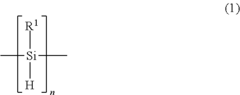
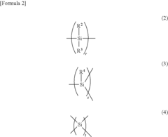
- Incorporating a small amount of cyclic polysilane into the top surface layer of the electrophotographic photosensitive element, specifically a polysilane represented by the formula (1), which enhances lubricity and cleaning properties while maintaining mechanical strength and transparency.
Environmental Impact of Polysilane-based Photonic Materials
The environmental impact of polysilane-based photonic materials is a crucial aspect to consider as these materials gain prominence in various applications. Polysilanes, known for their unique photonic properties, have the potential to revolutionize optical and electronic devices. However, their widespread adoption raises concerns about their ecological footprint throughout their lifecycle.
The production of polysilanes involves chemical synthesis processes that may generate hazardous byproducts and consume significant energy. The use of silicon-based precursors and organic solvents in the manufacturing process can lead to the release of volatile organic compounds (VOCs) and other pollutants if not properly managed. Additionally, the energy-intensive nature of polysilane synthesis contributes to greenhouse gas emissions, particularly when relying on non-renewable energy sources.
During the use phase, polysilane-based photonic materials generally exhibit low environmental impact due to their energy-efficient properties in optical and electronic applications. Their ability to manipulate light effectively can lead to reduced power consumption in devices, potentially offsetting some of the environmental costs associated with their production.
End-of-life considerations for polysilane-based materials present both challenges and opportunities. The complex nature of these materials may complicate recycling efforts, potentially leading to increased electronic waste if not properly managed. However, research into sustainable disposal methods and recycling techniques for silicon-based polymers shows promise for mitigating these concerns.
The potential for bioaccumulation and persistence of polysilane derivatives in the environment is an area that requires further investigation. While silicon is generally considered non-toxic, the long-term effects of novel polysilane structures on ecosystems and human health are not yet fully understood. This uncertainty underscores the need for comprehensive lifecycle assessments and environmental monitoring as these materials become more prevalent.
Efforts to improve the environmental profile of polysilane-based photonic materials are ongoing. Green chemistry approaches, such as the development of water-based synthesis methods and the use of renewable precursors, aim to reduce the environmental impact of production processes. Additionally, research into biodegradable polysilane derivatives could address end-of-life concerns and promote a more circular economy for these materials.
As the field of polysilane-based photonics advances, it is crucial to balance technological progress with environmental stewardship. Implementing sustainable practices throughout the material's lifecycle, from production to disposal, will be essential for realizing the full potential of polysilanes while minimizing their ecological footprint. Continued research and collaboration between materials scientists, environmental experts, and industry stakeholders will be key to developing environmentally responsible solutions in this promising field of photonic materials.
Scalability and Commercialization Prospects
The scalability and commercialization prospects of polysilane's photonic properties present both opportunities and challenges. As research progresses, the potential for large-scale production and practical applications becomes increasingly apparent.
One of the key factors driving scalability is the development of more efficient synthesis methods. Traditional polymerization techniques often result in low yields and limited control over molecular weight distribution. However, recent advancements in catalytic polymerization and controlled radical polymerization show promise for producing high-quality polysilanes at scale. These improved methods could significantly reduce production costs and increase the feasibility of commercial applications.
The unique photonic properties of polysilanes make them attractive for various commercial applications. In the field of photonics, polysilanes could be used to develop novel optical devices, such as waveguides, sensors, and light-emitting diodes. The ability to tune their optical properties through structural modifications opens up possibilities for customized solutions in different industries.
Another promising area for commercialization is in the development of photoresists for lithography. Polysilanes' high sensitivity to UV light and their ability to form stable patterns make them excellent candidates for next-generation photoresist materials. This could have significant implications for the semiconductor industry, potentially enabling the production of smaller and more efficient electronic components.
The integration of polysilanes into existing manufacturing processes presents both opportunities and challenges. While their unique properties offer potential improvements in various applications, adapting current production lines to incorporate these materials may require substantial investment. This could initially limit adoption to high-value applications where the benefits outweigh the costs of implementation.
Environmental considerations also play a role in the commercialization prospects of polysilanes. As industries increasingly focus on sustainability, the biodegradability and low toxicity of some polysilane derivatives could be advantageous. However, further research is needed to fully understand their environmental impact and develop eco-friendly production methods.
Market acceptance and regulatory approval will be crucial factors in the successful commercialization of polysilane-based products. Demonstrating the safety and reliability of these materials in various applications will be essential for gaining consumer trust and meeting regulatory requirements. Collaborative efforts between academia, industry, and regulatory bodies will be necessary to address these challenges and unlock the full commercial potential of polysilanes' photonic properties.
Unlock deeper insights with Patsnap Eureka Quick Research — get a full tech report to explore trends and direct your research. Try now!
Generate Your Research Report Instantly with AI Agent
Supercharge your innovation with Patsnap Eureka AI Agent Platform!